#quick turn PCB fabrication
Explore tagged Tumblr posts
Visit Tumblr Blog
Explore Tumblr blogs with no restrictions, modern design and the best experience.
Last Seen Tumblr Blogs


Fun Fact
70% of Tumblr users say the Dashboard is their favorite place to spend time online.
Text
Trusted PCB Manufacturing Companies in India
Pcbcircuit is well-known fast-growing Pcb manufacturer in india. We are committed to excellence, sustainability, and customer satisfaction”. We strive to provide our customers with the highest quality and most reliable PCBs that can withstand rigorous applications.

#pcb fabrication#low-cost pcb manufacturer#flex pcb manufacturer#pcb manufacturer in haryana#quick turn pcb fabrication
2 notes
·
View notes
Text
PCB Assembly Precision and Performance For Every Project
A PCB assembly company in Hyderabad specializes in manufacturing and assembling printed circuit boards (PCBs) for various industries such as electronics, automotive, and telecommunications. These companies offer services including PCB design, prototyping, component sourcing, assembly, and testing, serving both small-scale and large-volume production needs.

#top 10 pcb manufacturer#pcb fabrication#quick turn pcb fabrication#pcb stencil#pcbcircuit#low-cost pcb manufacturer
0 notes
Text
Top PCB Manufacturer in India
PCBcircuit is a leading PCB manufacturer in India, offering high-quality printed circuit boards tailored to diverse industries. With advanced technology, precision engineering, and reliable customer support, we ensure efficient and cost-effective PCB solutions to power your innovations. Trust PCBcircuit for quality and excellence in PCB manufacturing.

#flex pcb manufacturer#prototype pcb manufacturing#pcb manufacturer#custom pcb manufacturing#low-cost pcb manufacturer#pcb fabrication#quick turn pcb fabrication#high-quality pcb manufacturing#multilayer pcb manufacturer
0 notes
Text
Best Pcb Manufacturer Company in Bombay
Looking for the best PCB manufacturer in Bombay? Pcbcircuit is your go-to choice, offering high-quality, reliable, and cost-effective PCB solutions. With state-of-the-art technology and a dedicated team of experts, We ensures precision, durability, and prompt delivery for all your electronic needs. Trust Pcbcircuit for unparalleled service and top-notch products in the industry.

#prototype pcb manufacturing#quick turn PCB fabrication#Best pcb stencil maker in hyderabad#Two layer pcb stencil#Pcb stencil#Pcb manufacturer in delhi#pcbcircuit
0 notes
Text
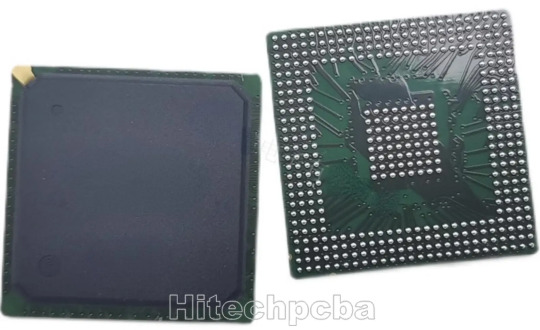
BGA PCB Assembly
What’s BGA PCB?
BGA PCB is Printed Circuit Boards with Ball Grid Array. We use various sophisticated techniques for making BGA PCBs. Such PCBs have a small size, low cost, and high packaging density. Hence, they are reliable for high-performance applications.

What’s BGA PCB Assembly?
Ball Grid Array (BGA) assembly technology is a surface mount packaging technology applied to integrated circuits, which is often used to permanently fix devices such as microprocessors. BGA assembly can accommodate more pins than other packages such as Dual in-line packages or Quad Flat Packages, and the entire bottom surface of the device can be used as pins , instead of only peripherals available, and also have a shorter average wire length than peripheral-limited package types for better high-speed performance.
Our BGA assembly services cover a wide range, including BGA prototype development, BGA PCB assembly, BGA component removal, BGA replacement, BGA rework and reballing, BGA PCB assembly inspection, and so on. Leveraging our full-coverage services, we can help customers streamline the supply network and accelerate product development time.
Benefits of BGA PCB Assembly
Efficient Use of Space – BGA PCB layout allows us to efficiently use the available space, so we can mount more components and manufacture lighter devices.
Better Thermal Performance – For BGA, the heat generated by the components is transferred directly through the ball. In addition, the large contact area improves heat dissipation, which prevents overheating of components and ensures long life.
Higher Electrical Conductivity – The path between the die and the circuit board is short, which results in better electrical conductivity. Moreover, there is no through-hole on the board, the whole circuit board is covered with solder balls and other components, so vacant spaces are reduced.
Easy to Assemble And Manage – Compared to other PCB assembly techniques, BGA is easier to assemble and manage as the solder balls are used directly to solder the package to the board.
Less Damage to Leads – We use solid solder balls for manufacturing BGA leads. Hence, there is a lesser risk that they will get damaged during the operation.
In a word, BGA PCB assembly, have these advantages, high density, better electrical conductivity, lower thermal resistance, easy to assembly & manage are some of the advantages of BGA PCB.
Stringent BGA PCB Assembly Testing Process
To achieve the highest quality standards for BGA assembly, we use a variety of inspection methods throughout the process including optical inspection, mechanical inspection, and X-ray inspection. Among them, the inspection of BGA solder joints must use X-rays. X-rays can pass through the components to inspect the solder joints below them, so as to check the solder joint position, solder joint radius, and solder joint thickness.
Inspection of BGA PCB
We mostly use X-ray inspection for analyzing the features of BGA PCBs. This technique is known as XRD in the industry and relies on X-rays for unveiling the hidden features of this PCB. This kind of inspection reveals.
* Solder Joint Position
* Solder Joint Radius
* Change in Circular shape
* Solder Joint Thickness

The Hitechpcba advantage lies in a whole range of aspects, beginning from the fact that we have the proven technology available at our disposal. With over 15 years of experience in a wide range of PCB Fabrication and Assembly techniques, what we also have is trained manpower and importantly, robust industry experience and best practices that you can benefit from.
Our unstinting devotion to quality and customer satisfaction means that once you partner with us, you can rest assured that you will get nothing but the best. The customer-oriented approach also shows up in your commitment to delivery times. With quick turnaround times, you can reap the benefit of quick time-to-market, which, in turn, can be a major source of competitive advantage.
Whether your requirement is BGA PCB design, BGA PCB, BGA PCB layout, BGA PCB Assembly or BGA rework, you can rest assured that you will get superior quality and performance, that will in turn, positively impact the performance of your final product.
With our efficient network of component suppliers and the many economies of scale that we enjoy, that you will get optimal costs, is a given.
Please feel free to contact us ([email protected]) if you have any other special request on the BGA pcb assembly.
3 notes
·
View notes
Text
Quick-turn PCB assembly refers to an assembly service that can manufacture and assemble printed circuit boards in a very short turnaround time, generally taking only 24 to 48 hours to complete. Choosing a reliable quick turn PCB assembler matters, which provides you with high-quality circuit boards within the shortest time. But it’s not easy to make the correct decision as there are many quick-turn PCB assemblers available in the market.
Here are some points to help you choose the best quick turn PCB assembly service.
Experience
Speed
Quality
Equipment
Costs
Know more at: https://aaloktronix.com/what-is-quick-turn-pcb-assembly-know-about-its-fabrication-and-manufacturers/
2 notes
·
View notes
Text
Fast Turn Pcb Fabrication
Fast turn PCB fabrication focuses on accelerating the manufacturing process to deliver high-quality printed circuit boards in record time. Using advanced automation, streamlined workflows, and precision engineering, this service enables rapid prototyping and quick production runs. Industries requiring urgent product development, such as IoT, medical devices, and telecommunications, benefit from fast turn PCB fabrication, ensuring they stay ahead in competitive markets with reliable and efficient solutions.
Fast Turn Pcb Fabrication
0 notes
Text

Low Cost PCB Circuit Board manufacturing
We provide printed circuit board fabrication with competitive prices for thousands of electronic design engineers, PCB assemblers, hobbyists and students from all over the world.
Three differences between us and other low-cost PCB manufacturers are as followed:
1. We provide higher quality boards with low cost which are made in China.
2. Faster lead time (24 hours for 2 layers PCBs prototypes and small batch production).
3. Superior customer service (Dedicated account rep, personal to personal).
As experts in the manufacture and assembly of printed circuit boards, we work to make our blog a helpful resource on PCB topics and the industries that we work with, including automotive, consumer electronics, aerospace and many more. Here you'll find insights into PCB design, tech trends, assembly issues, and trending topics in the general news media as they relate to printed circuit board technology.
Higher quality PCBs at a Lower Price
We can provide you with high quality domestic printed circuit boards that are not only at a low price, but also meet our stringent testing and quality standards. Every piece of printed circuit board will be tested before shipping. If you are ever unsatisfied with our low-cost PCB manufacturing services, we can quickly resolve any issues with our local in-house manufacturing capabilities and try our best to meet all your requirements. We aren't just providing you with "cheap PCBs", we are providing you with inexpensive PCBs that are of the highest quality! Don't be tricked by other discounted PCB factory, make sure you are still getting the board quality that your PCB prototyping efforts demand.
Are you looking for Cheap PCB Prototyping manufacturer in China?
Hitech Circuits manufactures printed circuit boards for the simplest 2 layer hobbyist projects to the most complex PCB to meet the rigorous requirements for military, medical, aerospace, etc. To satisfy the needs of our wide range of customers, we have created 3 different ways to order printed circuit boards: Standard Spec, Custom Spec, and our 2 & 4 Layer Prototyping Specials. The different categories help our customers stay on budget while making it easy to meet their project requirements
There is no shortage of PCB manufacturers that produce boards “on the cheap”. But how does their cheap PCB fabrication compare with our low cost prototyping options? Hitech Circuits’ experienced CAM engineers fully inspect your PCB design files before manufacturing, contacting you if there are any issues found. Unlike the “no-touch” alternatives, you are not left on your own with design issues after manufacturing with boards that you are not able to use. We also offers you:
Industry’s best on-time shipping record
Quick turn as fast as Same Day
100% China Based Manufacturing
Industry’s largest support team
24 Hr. tech support
Latest state-of-the-art equipment
High Quality Standards
Detailed CAM Review
Generally, PCB buyers choose a targeted PCB manufacturer based on the overall needs of the factory when choosing a PCB manufacturer. Professional PCB manufacturers produce PCBs with more quality assurance and low cost. Therefore, PCB buyers will choose PCB manufacturers with solid production and service capabilities to reduce the overall PCB procurement risk. However, it is not easy for PCB buyers to find a suitable PCB manufacturer, so how to choose a PCB manufacturer?
Let us understand how to choose the best China pcb manufacturer?
A: As a PCB manufacturer for hobbyist, PCB manufacturers near me is an important consideration
For example, PCB manufacturing USA, PCB manufacturing UKand PCB manufacturing Australia. China has more cheap PCB manufacturers. It is also a good idea to choose China PCB manufacturer.
B: Pay attention to the range of process capability and services.
PCB manufacturing process is complex and tedious; when choosing a PCB manufacturer, try to choose a PCB manufacturer with a wide range of functions and rich process capabilities so as not to delay the process involved beyond the ability of the PCB manufacturer, which will affect the PCB delivery time, so first when choosing a PCB manufacturer There must be a detailed reference to the PCB process requirements to prevent electrical functions from being affected due to the lack of PCB manufacturer's process.
C: Pay attention to whether the PCB manufacturer's production equipment can meet the requirements. Due to the different types of PCBs, the PCB production requirements are pretty additional, and the equipment levels used by PCB manufacturers are also different. Therefore, PCB manufacturers must make sample comparisons before considering batch cooperation.
D: Pay attention to whether there is a pegging fork clause. Due to the particularity of PCB custom processing, all PCBs that need to be assembled and shipped have a single probability of being scrapped. Generally, the customer accepts the pegging fork clause by default. If you do not buy it, you need to contact the PCB. The manufacturer communicates, usually, the PCB manufacturer will charge a certain fee, and you need to choose whether to accept the flat cross according to your situation.
E: Pay attention to whether the PCB manufacturer's quality assurance products. Regarding quality assurance, when choosing the best china pcb manufacturer, you must first judge the quality of the PCB manufacturer, such as whether the PCB has tested the PCB product before shipment to avoid the impact of quality problems. The later use of PCB prevents subsequent safety issues.
The main factors to calculate a pcb prototype price:
1. Board size: the larger dimension, the much expensive.
2. Materials: Some substrate and laminate PCB materials cost more than others. If high performance is essential, then your materials may be more expensive.
3. Complexity: Having a large number of components, complex wiring, or a very dense board can increase the overall cost.
3. Copper thickness: the heavier copper thickness, the much expensive price
4. Surface finished: usually HASL and OSP is the cheapeat, then silver, Tin, ENIG, ENEPIG is expensive
What is the Difference between Standard PCB and PCB Prototype?
Why suggest the PCB before choosing design Prototype PCB?
And what circumstances is PCB prototyping suggestion?
What are the advantages of PCB prototyping? You will find the answer below.
1. Quantity
The number of Prototypes PCB designs is far less than standard design products. Basically less than 10 or between 100 and 500.
2. Production Lead Time
Unless the delivery time of a single component is longer, the production lead time of the PCB prototype design will within 10 days.
3. Unit Cost and Total Cost
The total cost is much lower. PCB prototype design has many advantages beyond standard design.
Hitech Circuits is China PCB manufacturer. If you need PCB manufacturer with low price, please get in touch with us.
0 notes
Text
Fabricante de Placas de Circuito Impreso Flexibles-Rígidas
Las placas de circuito impreso (PCB) rígidos-flexibles se fabrican combinando tecnologías de placas rígidas y flexibles. Estas placas de circuito están formadas por múltiples capas internas de circuitos flexibles. Para unir estas capas internas se utiliza una película adhesiva epoxi preimpregnada. La principal ventaja de estas placas es que combinan la mejor calidad de las placas de circuitos flexibles y rígidos. Esto puede tener varias ventajas adicionales en lo que respecta a la estabilidad, el ensamblaje, la transmisión de señales y el tamaño general del circuito. HitechPCB proporciona una serie de variantes en las PCB rígidas-flexibles, que incluyen la flexión rígido de 4 capas con acabado ENIG, flexión rígido de 10 capas con flexión de 4 capas, flexión rígido de 12 capas con disipador de calor, tarjetas de circuitos flexibles rígidos de 14 capas, y muchos más. Es uno de los principales fabricantes de PCB rígida-flexible.
Cada placa de circuito impreso depende del cobre para transportar la electricidad. Entendemos que el espesor del cobre juega un papel clave en el rendimiento de estas placas de circuito. Por lo tanto, permitimos a los clientes elegir entre una variedad de espesores de cobre, incluyendo 0,5 OZ, 1,0 OZ, 2,0 OZ, 3,0 OZ, hasta 6 OZ. La máscara de soldadura contribuye a mejorar el aspecto estético de los componentes de la placa de circuito impreso. Podemos proporcionar placas de circuito impreso flex rígidos en varios colores de máscara de soldadura, incluyendo blanco, negro, azul, verde, rojo y blanco Taiyo PSR4000. La placa de circuito impreso puede suministrarse en colores de serigrafía: blanco y negro.
Las placas de circuito impreso flexibles rígidos tienen unos requisitos de espacio m��nimos que se optimizan mediante la aplicación 3D. Estas placas de circuito impreso no necesitan cables ni conectores entre las piezas rígidas. Esto ayuda a reducir el tamaño de la placa, así como el peso total del sistema. Estas menores juntas de soldadura también ayudan a garantizar una alta conectividad. Además, estas placas tienen contactos ZIF integrados. Estos contactos ayudan a simplificar la interconexión del sistema. Esta PCB rígida-flexible de 4 capas y otras placas de circuito impreso e envasan al vacío durante el transporte. Esto nos ayuda a asegurar la calidad, así como las condiciones de trabajo de las placas.
#PCB Rígida-Flexible
#PCB manufacturer
#PCB fabrication China
#custom PCB manufacturing
#prototype PCB manufacturing
#low-cost PCB manufacturer
#high-quality PCB manufacturing
#quick turn PCB fabrication
#flex PCB manufacturer
#multilayer PCB manufacturer
#Best pcb manufacturer
#Top 10 pcb manufacturer
#Pcb manufacturer near me
#Pcb manufacturer in China
#FPCB manufacturer
#PCB Assembly
#PCB Assembly China
0 notes
Text
Flexible PCB Manufacturer - Custom Solutions for Innovative Electronics
We specialize in designing and manufacturing high-quality flexible pcb manufacture (PCBs) tailored to meet the demands of diverse industries. Our expertise in flexible circuit technology enables us to produce durable, reliable, and compact PCBs for applications ranging from consumer electronics to medical devices, automotive, and more. With precision engineering, fast turnaround times, and advanced manufacturing processes, we provide customized solutions that drive innovation in your electronic products.
#best pcb manufacturer#flex pcb manufacturer#multilayer pcb manufacturer#pcb manufacturer in haryana#low-cost pcb manufacturer#pcb manufacturer#pcb manufacturer in delhi#quick turn pcb fabrication#pcb manufacturer in maharashtra#pcb manufacturer near me
0 notes
Text
Thinking About a PCB Prototype Service? Here’s Why You Should
Choosing a PCB manufacturing company with a dedicated PCB prototype service is crucial for product development. Prototyping allows engineers to test circuits, detect design flaws, and make improvements before moving to mass production. This process not only enhances efficiency but also reduces costly mistakes, ensuring the final product meets performance expectations. With rapid prototyping, businesses can confidently bring their innovations to market without unnecessary delays.
A well-structured quick-turn PCB assembly service helps accelerate production timelines while maintaining high quality. Whether for consumer electronics, automotive applications, or industrial solutions, having a reliable provider ensures your circuit boards are assembled with precision. Quick turnaround capabilities mean businesses can stay ahead of deadlines and respond to market demands faster, making it a game-changer for product development.
With advancements in printed circuit board fabrication, the process has become more refined and efficient. Using state-of-the-art technology, manufacturers produce durable, high-performance boards that meet industry standards. If you're looking for a smooth transition from design to production, a trusted prototyping and assembly partner is key. Read the blog & start optimizing your PCB development process today - https://sites.google.com/view/printed-circuit-boards-/blogs/thinking-about-a-pcb-prototype-service-heres-why-you-should
#pcb prototype service#quick turn pcb#prototype pcb fabrication#full turn key pcb#pcb manufacturing company#quick turn pcb fabrication#printed circuit board design software#pcb prototype manufacturer
0 notes
Text
India's Best Custom PCB Manufacturer - Pcbcircuit
We specialize in delivering high-quality, precision-engineered PCBs tailored to your exact specifications. From concept to final product, our team ensures top-notch reliability and innovation at every stage. Trust us to power up your electronics with industry-leading PCB solutions! Best PCB manufacturers are known for their experience, customer support, and ability to scale production based on project requirements.

#top 10 pcb manufacturer#pcb fabrication#quick turn pcb fabrication#pcb stencil#pcbcircuit#low-cost pcb manufacturer
0 notes
Text
Choosing The High-quality PCB Manufacturing in India
Pcbcircuit is a High-quality PCB manufacturing service in India. We offer precision-engineered printed circuit boards tailored to meet diverse industry needs. Ensure reliability, durability, and efficiency in your electronic projects by choosing our high-quality PCBs, designed to exceed global standards. Perfect for innovation-driven businesses.

#custom pcb manufacturing#pcb manufacturer#flex pcb manufacturer#low-cost pcb manufacturer#quick turn pcb fabrication#high-quality pcb manufacturing#pcb fabrication#prototype pcb manufacturing#multilayer pcb manufacturer
0 notes
Text
Optimized SMT Circuit Board and PCB Assembly Manufacturing: A Guide to Modern Electronics Production
In the ever-evolving world of hardware, the SMT (Surface Mount Technology) circuit board and PCB (Printed Circuit Board) assembly fabricating forms have gotten to be progressively vital. These advances not as it were empower the creation of smooth, compact, and high-performance electronic gadgets but moreover play an imperative part in the victory of different businesses, from shopper hardware to aviation and beyond.
Understanding the SMT Circuit Board Manufacturing Process
The SMT circuit board fabricating prepare includes the situation and fastening of electronic components specifically onto the surface of a printed circuit board. This approach offers a few focal points over conventional through-hole innovation, including:
1. Miniaturization: SMT components are by and large littler and more compact than their through-hole partners, permitting for the creation of littler and more lightweight electronic devices.
2. Increased Productivity: The robotized pick-and-place machines utilized in SMT fabricating can collect components on a circuit board much quicker than manual patching, moving forward generation efficiency.
3. Enhanced Unwavering quality: The patch joints in SMT gatherings are regularly more dependable and less inclined to disappointment than those in through-hole designs.
4. Cost Investment funds: SMT fabricating frequently decreases the in general fetched of electronic components and congregations, making them more open to a more extensive run of businesses and consumers.
The PCB Assembly Manufacturing Process
The PCB Assembly Manufacturing includes the integration of different electronic components onto a printed circuit board to make a useful electronic gadget. This prepare ordinarily incorporates the taking after steps:
1. PCB Manufacture: The to begin with step is the generation of the printed circuit board itself, which includes the creation of copper follows, cushions, and other highlights on a non-conductive substrate, such as fiberglass or ceramic.
2. Component Situation: Once the PCB is manufactured, electronic components, such as resistors, capacitors, coordinates circuits, and connectors, are put onto the board utilizing computerized pick-and-place machines or manual assembly methods.
3. Soldering: After the components are set, they are fastened onto the PCB utilizing procedures like wave patching, reflow patching, or specific fastening, depending on the particular necessities of the assembly.
4. Inspection and Testing: The amassed PCB is at that point assessed and tried to guarantee that all components are legitimately associated, and the circuit is working as intended.
5. Finishing Forms: Depending on the application, the PCB may experience extra wrapping up forms, such as conformal coating, embodiment, or the expansion of warm sinks or shielding.
The Significance of SMT Circuit Board andPCB Assembly Manufacturing
The SMT Circuit Board and PCB assemblyfabricating forms are basic for the generation of a wide run of electronic gadgets, from shopper hardware to mechanical hardware and past. These advances empower the creation of compact, lightweight, and profoundly solid electronic components and congregations, which are basic for assembly the ever-increasing request for progressed, feature-rich electronic devices.

Furthermore, the SMT circuit board and PCB gathering fabricating forms play a pivotal part in the competitiveness of different businesses, as they permit for the quick and cost-effective generation of electronic items. This, in turn, leads to progressed time-to-market, diminished fabricating costs, and upgraded item quality, all of which are basic for keeping up a competitive edge in today's worldwide marketplace.
Conclusion
The SMT circuit board and PCB assemblyfabricating forms are at the heart of the advanced gadgets industry, empowering the creation of imaginative and mechanically progressed items that proceed to change our world. By understanding the complexities and benefits of these forms, producers and originators can use these advances to make items that are not as it were outwardly engaging and profoundly useful but too cost-effective and dependable.
0 notes
Text
Optimize Your Electronics with SMD PCB Assembly and Fast Turn PCB Fabrication
In today’s fast-paced world, where electronics power almost every aspect of our lives, having efficient and reliable circuit boards is paramount. Two key components that ensure the success of your electronic products are SMD PCB assembly and fast turn PCB fabrication. Whether you're creating consumer gadgets, industrial equipment, or automotive systems, these processes play a crucial role in the development cycle.
This article dives deep into why SMD PCB assembly and fast turn PCB fabrication are essential for modern electronic manufacturing. We’ll explore how these processes improve efficiency, reduce costs, and help businesses bring high-quality products to market faster than ever before.
Understanding SMD PCB Assembly
Surface Mount Device (SMD) PCB assembly is a method used to attach electronic components directly onto the surface of a printed circuit board (PCB). Unlike traditional through-hole technology, which requires drilling holes for components, SMD assembly streamlines the process, making it faster and more efficient.
https://morepcb.com/wp-content/uploads/2023/01/bg_2.webp
Key Benefits of SMD PCB Assembly:
Compact Designs: SMD technology enables the use of smaller components, allowing manufacturers to design compact and lightweight devices. This is particularly valuable in industries like smartphones, wearables, and medical devices.
Increased Automation: SMD assembly relies heavily on automated machines, reducing manual labor and increasing precision. This results in fewer errors and consistent quality across production runs.
Cost Efficiency: By utilizing smaller components and automation, manufacturers can lower production costs, making SMD assembly an economically viable option for small and large-scale projects.
Improved Performance: The shorter leads in SMD components reduce resistance and inductance, improving signal integrity and enhancing overall device performance.
For businesses looking to stay competitive, adopting SMD PCB assembly is a strategic move. It ensures that your electronics meet modern standards without compromising on quality or reliability.
The Role of Fast Turn PCB Fabrication
In addition to SMD PCB assembly, fast turn PCB fabrication is critical in today’s competitive landscape. Fast turn fabrication refers to the accelerated production of PCBs, enabling companies to reduce lead times and respond quickly to market demands.
Why Choose Fast Turn PCB Fabrication?
Shortened Development Cycles: With fast turn services, you can prototype, test, and refine your designs in record time. This agility is especially important in industries like consumer electronics, where innovation moves quickly.
Quick Market Entry: Launching your product ahead of competitors can make a significant difference. Fast turn PCB fabrication ensures that your designs are production-ready in days instead of weeks.
Enhanced Flexibility: Manufacturers offering fast turn services can adapt to changes in design or volume requirements, giving you the flexibility to scale your production as needed.
Improved Cash Flow: Faster production means quicker product launches, which translates to earlier revenue generation and improved cash flow for your business.
When paired with SMD PCB assembly, fast turn PCB fabrication becomes a powerful tool for delivering high-quality products on time, even under tight deadlines.
How to Leverage Both Processes
Combining SMD PCB assembly and fast turn PCB fabrication is the ultimate strategy for achieving efficiency in electronic manufacturing. Here’s how you can make the most of these processes:
Partner with a Reliable Manufacturer: Look for a provider with a proven track record in SMD PCB assembly and fast turn PCB fabrication. Check reviews, ask for samples, and ensure they use state-of-the-art equipment.
Optimize Your Design for Manufacturing (DFM): Work closely with your manufacturer to optimize your PCB design for both assembly and fabrication. This minimizes errors, reduces costs, and ensures a smooth production process.
https://morepcb.com/wp-content/uploads/2023/02/pcb-asembly.png
Invest in Prototyping: Use fast turn services for rapid prototyping. This allows you to test your designs, identify potential issues, and refine your product before mass production.
Choose Quality Materials: High-quality PCBs require top-notch materials. Ensure your manufacturer uses reliable substrates, copper cladding, and solder masks to meet industry standards.
Utilize Advanced Technology: The latest technologies, such as automated pick-and-place machines and X-ray inspection, ensure precision in SMD assembly and fabrication.
Real-World Applications of SMD PCB Assembly and Fast Turn Fabrication
Consumer Electronics: From smartphones to smartwatches, compact and high-performance PCBs are essential. SMD PCB assembly ensures miniaturization, while fast turn fabrication keeps up with demand.
Automotive Industry: Modern vehicles rely heavily on PCBs for everything from engine control to infotainment systems. These industries benefit from quick turnaround times to meet production schedules.
Medical Devices: Precision and reliability are critical in medical equipment. Fast turn PCB fabrication allows for rapid prototyping and stringent quality checks, while SMD assembly ensures compact, efficient designs.
Aerospace and Defense: Complex, high-performance PCBs are vital in these industries. SMD assembly supports advanced designs, while fast turn fabrication meets the demand for quick deployment.
Final Thoughts
The combination of SMD PCB assembly and fast turn PCB fabrication is a game-changer for businesses aiming to deliver high-quality electronic products quickly and efficiently. By leveraging these advanced manufacturing processes, you can reduce lead times, cut costs, and improve product reliability—all of which are essential for staying competitive in today’s fast-evolving markets.
To ensure success, partner with a reputable manufacturer who specializes in both SMD assembly and fast turn fabrication. With the right team and tools, you’ll not only meet your project deadlines but also exceed expectations in performance and quality.
Invest in SMD PCB assembly and fast turn PCB fabrication today to unlock the full potential of your electronic products!
0 notes
Text

High Density PCB board (HDI PCB) Manufacturer & Assembly – One-stop services
What’s HDI PCB?
High-density interconnect (HDI) PCBs are characterized by finer lines, closer spaces, and more dense wiring, which allow for a faster connection while reducing the size and bulk of a project. These boards also feature blind and buried vias, laser ablated microvias, sequential lamination, and via in-pads.
As a result, a HDI board can house the functionality of the previous boards used. HitechPCB is an HDI PCB manufacturer and provider in Shenzhen,Chinasupports HDI PCB prototype and mass production with less expensive price and quick-turn lead time. Customers from a variety of industries we serve have a common that have high expectations in quality, reliability and on-time delivery in HDI PCB production. Our quality is not afterthought, but built into each process from front-end to fabrication and shipping.
HDI PCB Manufacturing Process
The overall process for manufacturing HDI PCB is essentially the same as for fabricating other PCB board, with notable differences for PCB stack-up and hole drilling. Since HDI boards generally require smaller drill holes for vias, laser drilling is usually required. Although laser drills can produce smaller and more precise holes, they are limited by depth. Therefore, a limited number of layers can be drilled through at a time. For HDI boards, which are invariably multilayer and may contain buried and blind vias, multiple drilling processes may be required. This necessitates successive layer boding to achieve the desired stack-up or sequential lamination cycles. Not surprisingly, this can significantly increase PCB manufacturing time and cost.
HDI PCB fabrication is an advanced technology and therefore requires expertise along with specialized equipment like laser drills, laser direct imaging (LDI) capability, and special clean room environments. In order to efficiently manufacture high-quality and reliable HDI PCB products, you must understand the HDI board manufacturing process and coordinate with your HDI PCB supplier to implement good DFM (Design for Manufacturability) for HDI layout design.
HDI Printed Circuit Board Development
HDI printed circuit boards were developed from a need to provide an increased level of computational power and performance in a smaller envelope. This need was driven largely by industries such as telecommunications, where the push to provide smaller and more powerful mobile phones necessitated finding a way to package more electronic circuitry in a smaller, denser package. However, other key drivers in the development of HDI PCBs were the trends in Integrated Circuit (IC) technology that acted as a forcing function to reconsider how printed circuit board layouts and interconnects were designed. Some of these key IC technology trends include:
The shrinking size of gates
Reduction in die size
Reduction in operating voltage levels to control power dissipation
Higher levels of gate integration (i.e. more transistors per unit area on a die)
Faster signal rise times (higher operating frequencies and clock rates)
The trend in the packaging of ICs has also shifted away from the use of low-count peripheral lead frame packages towards surface mount technology, allowing the placement of interconnecting pins underneath the entire surface area of the IC. One such technology is the Ball Grid Array (BGA), which places the interconnecting pins in a grid pattern on the underside of the IC. As more and more pins are added to the IC packages, the corresponding density of pins increases, and the dimensional spacing for the circuit board traces or pads decreases (known as the pitch). While this helps with the objective of shrinking the package size for the electronics, it also adds challenges and necessitates changes to the manufacturing process for HDI PCBs.
BGAs do have other advantages, such as lower thermal resistance between the device and the PCB. This fact helps with maintaining acceptable device operating temperatures for chips that are increasingly complex in terms of transistor density. Another advantage of grid array packaging is that the interconnecting leads are shorter. Shorter leads reduce inductance in the leads, which mitigates signal distortion in high-speed circuits, improving overall performance.
Advantages of HDI Printed Circuit Boards
HDI technology provides several advantages and benefits for designers and engineers.
Compact design – HDI boards have high wiring capacity and can reduce both the size and the number of layers needed to produce a design versus using traditional PCBs.
The use of micro vias and via in pad technology allows for components to be placed closer together and more components to be mounted on one side of the board, resulting in faster signal transmission and improved signal integrity due to shorter signal paths.
Laser drilling produces smaller holes and improves the board’s heat resistance.
The ability to reduce the number of layers needed in the PCB design can result in lower costs.
Low pitch devices such as BGAs whose pitch may be 1 mm or less can be supported.
The lower aspect ratio in HDI vias improved the plating of vias and overall board reliability.
Applications for HDI Printed Circuit Boards
HDI printed circuit boards have enabled more electronics to be packed into a smaller envelope, helping to reduce the size of products in a number of markets. Some example of HDI PCB applications include:
Healthcare and medical – implanted devices such as cardiac pacemakers and external devices such as hearing aids.
Automotive industry – smaller, lighter electronics save space and reduces vehicle weight.
Consumer devices – cellular phones, tablets, laptop computers, and touch screen products have all been reduced in size and weight with increased performance due to HDI technology.
Aerospace – electronic designs for missile systems, aircraft, and defense applications utilize HDI printed circuit boards that provide reliable operation in extreme environmental conditions.
0 notes