#full turn key pcb
Explore tagged Tumblr posts
Visit Tumblr Blog
Explore Tumblr blogs with no restrictions, modern design and the best experience.
Last Seen Tumblr Blogs


Fun Fact
If you dial 1-866-584-6757, you can leave an audio post for your followers.
Text
Reliable PCB Solutions: Fast Prototyping & Quick Turn Fabrication
Bringing electronic designs to life requires precision and speed, and quick-turn PCB fabrication plays a key role in making that happen. Whether you need a single board or a full production run, having a reliable manufacturing partner ensures high-quality results with faster turnaround times. Advanced fabrication techniques streamline the process, making it easier to meet project deadlines without compromising on performance.
For product development, a well-crafted prototype circuit board is crucial to testing functionality before full-scale production. With accurate prototyping, engineers can refine designs, identify potential issues, and optimize performance. Working with a trusted manufacturer simplifies the process, providing efficiency from concept to completion.Beyond fabrication, professional PCB assembly services take your boards from bare circuits to fully functional components. From precise component placement to thorough quality checks, expert assembly ensures reliability in every board. Get the best solutions for your PCB needs—start your order today!
#pcb manufacturing company#quick turn pcb fabrication#pcb prototype service#full turn key pcb#pcb prototype manufacturer
0 notes
Text
just ordered parts for a rough draft of a bug sweeper /o/
turns out it’s not that complex of an idea. just a spectrum analyzer and a highly directional antenna really. the key issue i’m expecting is designing an antenna array that covers the full bandwidth of interest. the tinySA covers 100k-5.3G, which is pretty broad and definitely too much for most antennas. the spiral antenna design looks promising though, especially if it could be done in a PCB, but it may still end up being pretty large to accommodate freqs down to 100 kHz. maybe a pair of a spiral plus something else more compact for low freqs will work better
2 notes
·
View notes
Text
Just How Carries Out A PCB Assembly Procedure Job?
The PCB assembly process begins with PCB fabrication, adhered to by part purchase. Parts are then put on the board utilizing automated pick-and-place devices. Solder insert is applied to connection parts during the course of reflow soldering. Inspection methods like AOI as well as practical testing ensure quality. Finally, panels are packaged for delivery after passing QC checks.
4 notes
·
View notes
Text


Printed circuit board manufacturing which is our major business, I think you already know, we are a PCB manufacturer. We have 3 branch factories dedicated to Quick Turn PCB Prototypes Manufacturing, Small and Medium-volume Printed Circuit Board, FPC Manufacturing services and PCB assembly services. Our market target is the High Multilayer PCB, High Density PCB, Flexible PCB, Rigid-flex PCB, Heavy copper PCB, Rogers PCB, Ceramic PCB and Special Materials Printed Circuit Boards.
Also, we can help customer sourcing components, wire PCB assembly and provide one-stop service.
Hitech Group is capable of providing full turn-key and partial turn-key PCB assembly services. For full turn-key, we take care of the entire process, including manufacture of Printed Circuit Boards, procurement of components, order tracking, continuous monitoring of quality and final board assembly. Whereas for partial turn-key, the customer can provide the PCBs and certain components, and the remaining parts will be handled by us.
4 notes
·
View notes
Text
A controller with a scroll wheel, you say?
Well this is a little funny. Yesterday I posted the first part of a series of post on the fine details of how computers work, mentioning how I've been looking into this as part of a personal project I've been working on, and today I wake up to see Masahiro Sakurai posting a youtube video lamenting the lack of... this exact thing I'm working on.
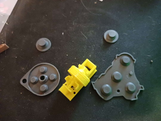
Apologies for how much cat hair is in this photo, that's a bit of an occupational hazard, but this here is a photo I took back in September when most of the parts I had to order were in for the prototyping of this thing:
That's a really bad MS Paint mockup, but yeah. I'm designing my own game console, and one of the key features is a big ol' scroll wheel right in the center of the controller. Another is that I'm planning to just put all the designs of the circuit boards and 3D printer files for the casing/buttons up online for free, making it this totally open DIY thing where anyone who's a big enough nerd can just make a couple downloads, order some dirt cheap components, and build their own copy of the system (or people with better setups than me can build and sell them, whatever). So I'm not super worried about anyone stealing my ideas or whatever, but I WOULD like to establish a standard and all that, and figured it was worth noting that this is something I've been slowly working towards for like a year or two now, and didn't just get the idea from this video:
youtube
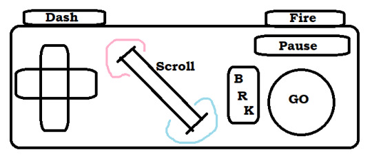
But yeah, now that the idea's out in the public consciousness, here's the plan for the controller (that I was planning to keep under my hat until I had a working prototype and some demo software sometime next year).
First off, the plan is that this is to be the standard controller for a whole console I'm also plucking away at designing, which is a bit more ambitious of a project, so I figure I might as well make it compatible with something that's already out there. So specifically, I'm designing this so that you can take one, plug it right into an SNES (or with a different connector at the end, an NES, because turns out they use the exact same input handling standard and it's just the shape of the plastic on the end that differs), and have it just work. Or mostly work anyway. I'm hoping I can process a signal out of the scroll wheel in a way that it either just needs the 3 extra bits of the input signal I don't have buttons for in my design (more on that later) or failing that, I can get it to output the same sort of signal as one wheel in the SNES mouse, which just rides along the second data line very few things use. I think that plan might break multitap compatibility and require an extra chip on the controller PCB, but it would leave this slightly more compatible with existing games on the same hardware. I might also do something weird with the button mapping to be sure NES select is on a shoulder and it works right out of the box with that whole library.
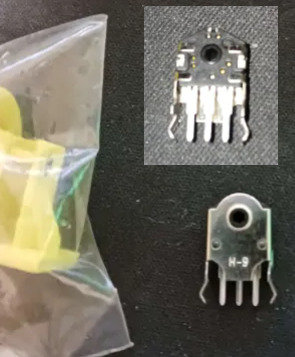
Working out exactly how to handle signals from the scroll wheel happens to be the point I'm currently stuck on by the way. I got this baggie full of rotary encoders for just a few cents which... almost fit in my first draft 3D printed wheel housing, but I have NO documentation on them, not even a part number/manufacturer besides "H-9," the pins don't fit a breadboard, and I've kinda been scrambling for rent so I can't afford a nice multimeter or oscilloscope to poke around with. Plus again I need to redesign this wheel print to even get it to spin right, and... this was a gift from a friend with a printer who is Not Local. Solvable problem, just needs more time and/or outside expertise.
But yeah, once I have those kinks worked out, it should be easy enough to get a custom board design made, replicas of end-cap of the controller cord are another problem easily solved by ordering a 1 dollar part or 3D printing something. The actual cord might be tricky since I don't know where you actually order something like that from, but it should be easy enough for anyone who doesn't mind a little assembly work to put one of these together and have it good to go for any software made with it in mind, or retrogames where you don't mind a weird button count. So... what's the pitch on this scroll wheel anyway?
Well for starters, there's the stuff Sakurai got into this morning. Any sort of RPG or text heavy game can use it to quickly scroll through menu options, or stuff in a text-heavy game. You could also pan the screen with it, something a lot of early 16-bit games assigned to the shoulder buttons or holding up and down while getting used to the new options the hardware was giving them.
Past that, you'll notice in my design it's at a 45 degree angle. I might have to tweak it a little, but my thinking is for a game that uses it heavily, one thumb or the other can slide over easily enough (I'm going for a pretty compact overall design) so we can have some games where you take your thumb off the D-pad, and have this nice analogue steering wheel. Nice for fine control in a racing game, or if you want some little radio-tuning/safe-cracking sorta deal.
Alternatively, move your right thumb over, use the D-pad to steer, shoot and dodge or whatever with shoulder buttons, and use the wheel to rotate a turret for a twin-stick sort of game maybe.
Or just use it for the sort of stuff mouse based games stick on the scrollwheel. Changing weapons, changing powerups... I'm planning to officially label the directions "hot" and "cold" to encourage weird gimmicky things like... I dunno, a platformer where you have a thermostat in your controller you can always mess with, freeze water coming out of pipes, crank up flame jets? Have a shot charging mechanic where you just really crank it to get to max strength? Weird minigame stuff. There's some fun space to explore with it.
Then we have the rest of the design here... which basically comes down to me being just plain sick of how every controller made by anyone in the past... 20 years give or take has kind of the exact same layout? 4 good face buttons, a D-pad, 4 shoulder buttons, 2 sticks, and 1-4 annoying to reach tiny awkward middle buttons, and we're just kind of overdue for a change-up?
Like first of all, hey, this is just too many buttons. There's a ton of games that really only need a D-pad, and maybe 3 buttons (attack jump pause) and the two things that aren't fully standardized is how awkwardly placed the D-pad is and how awful and awkwardly placed the pause button is. Shoulder buttons can be nice, but I've never really felt like 4 of them awkwardly crammed on the rim has been really useful or ergonomic, and that's coming from someone who's been playing a ton of FF14, which gets more use out of them than anything else I could name. And really, aside from games doing fake twin-stick stuff and using the whole grid like a second D-pad, I'm having a really hard time thinking of any game I've ever played that really makes good use of 4 good face buttons? Like people will use them if they've got'em sure, but unless you do that keyboard style thing where you lay the controller on a table and use all your fingers, you can really only comfortably hit 2 face buttons without sliding your thumb away from them, maybe comfortably make a quick pivot to a third.
Also, really, a lot of designers just sort of feel compelled to map SOMETHING to every button, even if it's clear the design didn't really need them. So basically I figure I'll try kinda just taking a "less is more" approach here. Here's the buttons that it's comfortable to rest your thumbs and fingers on, here's a dedicated pause/menu button where people often stick a kind of redundant menu button, here's my gimmicky scrollwheel. That's it, work around that.
I'm also going a little Gamecube inspired (literally using replacement membranes for one in my prototype design, even). Gonna make a great big primary button and use different shapes for the other two. Trying to label these in a less arbitrary fashion than most. If shooting a gun is a thing you do in this game, and there isn't a real good reason not to, default it to this nice right trigger you can hold down all the time. If we're advancing through menus or jumping or holding down gas in a car, here's the big GO button. Need brakes, need to break stuff with a melee attack? Go back in a menu system? There's your other face button. Have a quick dash move or a run you hold down, let's just use the other shoulder.
So yeah. That's my controller. Need to work out the kinks on the scroll wheel, source a cord, and hopefully I can slap things together and this will be something you can just order bits for piecemeal and put together for like, $5-10 after shipping? Maybe less? The parts are shockingly cheap so far.
But yeah if anyone has any insight to the scroll wheel or cord issues, let me know. Also the whole thing is presently a tad back-burnered because I am in a serious financial crisis and I don't want to have electronics spread all over my table if I have to abruptly find a new place to live if I can't scrape next month's rent together. So as usual, donations are incredibly welcome.
2 notes
·
View notes
Text
Streamlining Electronics Production: How to Choose the Right PCB Assembly Manufacturer
In today’s fast-paced electronics industry, selecting the right PCB assembly manufacturer is critical to product performance, speed to market, and overall success. Whether you're developing consumer electronics, industrial systems, or IoT devices, a reliable partner for PCB board assembly and PCB manufacturing assembly ensures quality, consistency, and scalability.
This article will guide you through what to look for in a dependable manufacturer and how the right choice can simplify your electronics production process from design to delivery.
1. What Does a PCB Assembly Manufacturer Do?
A PCB assembly manufacturer is responsible for soldering components onto a printed circuit board (PCB) to build a fully functioning electronic assembly. This includes handling both surface-mount technology (SMT) and through-hole technology, depending on the design requirements.
Top-level assembly services often include:
Component sourcing and inventory management
SMD and through-hole component placement
Reflow and wave soldering
Functional testing and inspection
Final packaging and delivery
When choosing a partner, ensure they offer comprehensive PCB manufacturing assembly under one roof—this minimizes errors, reduces turnaround time, and simplifies communication.
2. Understanding the PCB Board Assembly Process
The PCB board assembly process involves several critical stages:
Stencil printing: Applying solder paste to the PCB using a stencil
Pick-and-place: Automated machines place components with high precision
Soldering: Typically done through reflow or wave soldering methods
Inspection: AOI (Automated Optical Inspection), X-ray (for BGAs), and manual checks
Testing: Functional and in-circuit testing to ensure proper performance
Each of these steps requires advanced machinery and expert oversight, making it essential to work with a manufacturer that has a proven track record and quality certifications such as ISO 9001 or IPC-A-610.
3. Benefits of Working with a Full-Service PCB Manufacturing Assembly Partner
A full-service PCB manufacturing assembly partner can manage your project from prototype to full-scale production. This has several benefits:
Speed: Faster time-to-market with streamlined production processes
Quality assurance: Consistent output with strict quality control standards
Cost-efficiency: Reduced overhead from consolidated services
Design support: DFM (Design for Manufacturability) feedback helps avoid costly errors early
Look for partners offering quick-turn PCB assembly services, low-volume prototyping, and high-volume scalability.
4. Key Features to Look for in a PCB Assembly Manufacturer
When evaluating manufacturers, ask these questions:
Do they offer both prototyping and volume production?
What is their standard lead time for PCB board assembly?
Can they handle complex, multi-layer boards?
Do they assist with sourcing hard-to-find components?
Are their facilities equipped for RoHS-compliant or lead-free production?
Also, check whether the manufacturer has experience in your specific industry—be it medical devices, automotive systems, consumer tech, or industrial automation.
Final Thoughts
Choosing the right PCB assembly manufacturer is more than a procurement decision—it’s a strategic partnership that impacts product quality, cost, and time to market. By partnering with a provider that offers end-to-end PCB board assembly and complete PCB manufacturing assembly services, you gain a competitive edge in both development speed and product reliability.
Whether you're an engineer, startup, or OEM, investing in the right assembly partner can make all the difference.
0 notes
Text
Deep Coat: Pioneering EMI & RFI Shielding Solutions for Over Four Decades
In today’s high-frequency, high-stakes electronic environment, electromagnetic interference (EMI) and radio frequency interference (RFI) can jeopardize the performance and reliability of critical electronic systems. That’s where Deep Coat comes in—a trusted name in the EMI and RFI shielding industry since 1981. With a singular focus on delivering high-performance shielding solutions, Deep Coat has become an industry leader in vacuum metallization and electromagnetic shielding for military, medical, and commercial applications.
The Legacy of Deep Coat
Founded with a mission to engineer superior EMI shielding, Deep Coat has continuously pushed the boundaries of innovation in the field. What began as a company producing shielding solutions for printed circuit boards has since evolved into a full-spectrum manufacturer of EMI and RFI shielding products. Today, Deep Coat’s advanced coatings are used in everything from military-grade PCB shields to large molded enclosures for medical equipment, electronic connectors, instrument housings, and communication systems.
With over 35 years of expertise, Deep Coat’s proprietary vacuum metalization process stands as a testament to the company’s commitment to precision, performance, and reliability.
Advanced Shielding with Vacuum Metalization
Deep Coat is best known for its unique vacuum metalization process—a method that allows up to four different layers of metals to be applied within a single vacuum draw. This capability is critical for creating custom shielding solutions that meet the precise needs of each application.
Using this technique, Deep Coat can apply metal layers ranging from 0.3 to 24 microns, even on highly complex plastic geometries. The result is a uniform, durable coating that ensures high-level EMI and RFI attenuation across a wide frequency spectrum.
The flexibility of this process allows Deep Coat to use a variety of metal combinations, helping customers maximize shielding effectiveness while maintaining material compatibility and adhesion integrity.
A Proven Leader in Adhesion Technology
One of the key challenges in vacuum metalization is ensuring consistent metal-to-substrate adhesion, especially on non-metallic or irregular surfaces. Deep Coat addressed this problem head-on with the development of “in-chamber” RF plasma pretreatment. This proprietary technique enhances the surface of plastics and other non-conductive materials before metal application, significantly improving adhesion and long-term durability of the coating.
This innovation—along with other patented technologies developed by Deep Coat—has helped the company deliver consistently high-quality shielding solutions where other providers may fall short.
The Patented 4-Layer Shielding System
Among Deep Coat’s many technological advancements is its patented four-layer shielding system, which includes:
A base layer of stainless steel for durability and corrosion resistance
Two intermediate layers of copper for superior conductivity and shielding
A final stainless steel overcoat for added protection and environmental resilience
This multi-metal design offers a perfect balance of electrical performance and mechanical toughness, making it ideal for mission-critical applications in aerospace, defense, telecommunications, and healthcare sectors.
Why Choose Deep Coat?
Clients turn to Deep Coat not only for its advanced engineering and patent-backed technologies, but also for its reputation for excellence and reliability. Here’s what sets Deep Coat apart:
Over 40 years of industry experience
Proven vacuum metalization techniques
Custom metal layer combinations to suit specific EMI/RFI performance requirements
Exceptional adhesion performance on even the most complex plastic components
Made-in-America quality with meticulous attention to detail
From early-stage design consultations to full production runs, Deep Coat works closely with OEMs and engineers to ensure that every solution meets or exceeds industry standards.
Serving Diverse Industries
Deep Coat’s shielding technologies are utilized across a wide range of industries. Common applications include:
Military electronics and PCB shields
Medical device enclosures and imaging equipment
Telecommunications gear including routers, radios, and receivers
Aerospace instruments and control systems
Consumer electronics and industrial control panels
Each application benefits from Deep Coat’s custom approach to material selection, metal layering, and surface preparation.
Looking Ahead: Innovation at the Core
While many companies rest on legacy, Deep Coat continues to invest in research and development to stay ahead of evolving EMI/RFI threats. The company’s team of engineers and materials scientists are always working to refine coating processes, explore new metal alloys, and meet the challenges of next-generation electronics.
Whether you’re designing a new product or looking to improve an existing one, Deep Coat has the experience, technology, and track record to deliver high-performance shielding solutions tailored to your exact needs.
Conclusion
Deep Coat stands as a pioneer in EMI and RFI shielding solutions. With patented processes, cutting-edge vacuum metalization technology, and a reputation built over four decades, Deep Coat is the partner of choice for engineers, product designers, and OEMs who require reliable, high-performance shielding. Explore how Deep Coat can support your next project—because when it comes to shielding sensitive electronics, only the best will do.
#emi shield#rfi#EMIcoatings#RFICoatings#metal coating#deep coat#electronicsprotection#electromagneticprotection#emiprotection
0 notes
Text
Your Trusted Partner for High-Reliability Electronic Manufacturing--Hitech Circuits
Printed Circuit Boards (PCBs) play a vital role in modern technology, serving as the foundation for nearly every electronic device we rely on daily. From smartphones and medical equipment to automotive systems and industrial machinery, PCBs are at the heart of innovation, enabling seamless functionality and advanced capabilities.
At Hitech Circuits, we specialize in providing high-quality PCB manufacturing and assembly services designed to meet the needs of diverse industries. With state-of-the-art technology, strict quality control, and a highly skilled team, we deliver solutions that combine reliability, precision, and efficiency.
We can provide turnkey electronic manufacturing services. The services include:
PCB Manufacturing from Prototyping to Mass Production
Components Purchasing at competitive prices
PCB Assembly(Mechanical & Electronic Components)
Shell customization and assembly
Function Testing
PCB Reverse Engineering
With the experiences of over 20 years in the electronics manufacturing industrial, we are devoted to providing superior services and have cooperated with many famous brands. The end customers we serve are in industries such as aerospace, medical & life sciences, industrial,military & defence.
If you want to know the prices from us, please email Pelina--Hitechpcb<[email protected]> Below is the guideline of basic information you are supposed to provide or specify:
Complete GERBER files including the Excellon Drill File
Quantities
Need expedited service or not(for PCB prototype onlly)
Panelization Requirements
Materials Requirements
Surface Finish Requirements
Board Thickness
Copper Thickness
Assembly Requirements (including full turn key)
Any Other Requirements
Don't know what any of these items are? Call us. We can help.(Phone Number: 86-18033061378 )
Your custom quote for PCB or PCBA usually will be delivered within 24 hours(working day). We will always do our best to meet your needs and get your quote returned to you as soon as possible.
0 notes
Text
PCB de base de cobre, PCB de base de cobre – Hitech Circuits Co., Limited
PCB de alumínio são PCB de substrato de metal isolado comum (IMSPCB) amplamente usados para luzes LED, iluminação automóvel e outras aplicações de alta condutividade térmica. A condutividade t érmica dos PCB de alumínio é geralmente 1W/mK ou 2W/mK. Se a condutividade térmica de um PCB de alumínio não pode satisfazer seus requisitos de aplicação esperados, por que não considerar PCB baseados em cobre?
Os PCB de base de cobre têm melhor condutividade térmica do que os PCB de alumínio e lhes proporcionam muito mais possibilidades de design.
Um PCB de base de cobre é um PCB de núcleo de metal com um substrato de cobre. Se um PCB híbrido cujo substrato é uma placa de cobre dentro da placa FR4, também é uma base de cobre PCB.
Normalmente, os PCB de base de cobre têm a mesma estrutura que os PCB de alumínio - uma camada, duas camadas com um lado de montagem de componentes, duas camadas com dois lados de montagem de componentes, e quatro camadas com dois lados de montagem de componentes. Mesmo eles usam o mesmo material prepreg para isolar as camadas de cobre. No entanto, o substrato de cobre (398W/mK) tem melhor condutividade térmica do que o substrato de alumínio (237W/mK).
What's more, there's thermoelectric separation technology (also called direct touch technology) for copper-base PCBs. Significa que, através da abertura de máscara de soldado e eletroplatagem de cobre para aumentar a espessura de cobre das posições necessárias, o calor conduz diretamente dos LED ou outros componentes para a base de cobre, enquanto a rede de circuitos é independente da rede térmica.
Se você tem uma pesquisa sobre PCB de núcleo metal, por favor contacte-nos livremente, obrigado.
Hitech Circuits Co., Limited
0 notes
Text
Anwendungen von Leiterplatten auf Kupferbasis
Leiterplatten auf Kupferbasis werden für Hochleistungsanwendungen, Anwendungen in Bereichen mit großen Temperaturunterschieden und Wärmeableitung für Präzisionskommunikationsgeräte verwendet. Und einige Anwendungen von Leiterplatten auf Kupferbasis sind:
LED-Leuchten: Leiterplatten auf Kupferbasis können für LED-Leuchten, insbesondere COB-LED-Leuchten verwendet werden. COB-LEDs können mit den LED-Platten durch Golddrähte oder Lötkugeln von PCBONLINE verbunden werden, und dann wird das LED-Modul auf der Kupferbasis-Leiterplatte aufgebracht, um die LED-Leuchten herzustellen.
Fahrzeugbeleuchtung: Für den Scheinwerfer von Fahrzeugen können beidseitig montierte Kupferplatinen verwendet werden. Die doppelseitige Kupferbasis-Leiterplatte bietet eine hohe Effizienz, hervorragende Wärmeableitung und einen überlegenen Strahlereffekt. Sowohl reguläre Leiterplatten auf Kupferbasis als auch thermoelektrische Trennplatinen können Automobilleuchten dienen.
Ladepfähle für Elektrofahrzeuge: Leiterplatten auf Kupferbasis können für Ladepfähle für Elektrofahrzeuge und HEVs verwendet werden. Zum Beispiel ist die Adapterplatine im Hochleistungs-Ladepfahl eine Kupfer/FR4-Hybridplatine. Aus Gründen der Zuverlässigkeit und Sicherheit werden im PCB-Design Großstrom- und Kleinstromschaltungen getrennt. Die Kupferplattenbereiche leiten große Ströme und leiten Wärme ab, und die FR4-Bereiche leiten kleine Ströme und Signale.
Schlussfolgerung
Kupferbasierte Leiterplatten haben eine gute Wärmeleitfähigkeit und werden für Hochleistungsgeräte und -systeme eingesetzt. Es gibt reguläre Kupferbasis-Leiterplatten mit 1W/mk bis 9W/mk Wärmeleitfähigkeit und thermoelektrische Trennkupferbasis-Leiterplatten mit 398W/mk Wärmeleitfähigkeit. Für die Herstellung und Montage von Leiterplatten auf Kupferbasis können Sie den One-Stop-Hersteller Hitech Circuits Co., Limited in Betracht ziehen, der vom Prototyp bis zur Massenproduktion herstellen und Ihnen eine kostengünstige und qualitativ hochwertige Fertigung anbieten kann.
Wenn Sie Metallkern PCB Anfrage haben, kontaktieren Sie uns bitte frei, danke.
Hitech Circuits Co., Limited
0 notes
Text

Turnkey PCB Assembly Manufacturer
Turnkey Circuit Board Assembly Manufacturer -- Hitech Circuits Co., Limited
What’s mean for Turnkey PCB Assembly?
Turnkey means a product or service that is ready for immediate use for the buyer and when applied to PCB assembly, this refer to the SMT factory will handle all steps for PCB assembly. Turnkey PCB assembly is including the entire steps complex in making a PCB, beginning from the fabrication process all the time to the assembly process.
In PCB manufacturing, turnkey PCB assembly also means the electronic manufacturing service, since it takes hands of the entire process of designing, manufacturing, and testing the printed circuit board.
Essentially, a full turnkey solution makes you to have enough time and focus on designing PCB, and our SMT factory can handle the rest of the steps and procedures. Turnkey solutions offer an efficient and cost-effective way to assemble and test circuit boards for products. This also offers companies a way to receive printed circuit boards with the shortest lead times possible.
Turnkey PCB assembly & manufacturing is the optimal solution for engineers with urgent, high complexity projects who want to avoid project management headaches. Providing turnkey PCB assembly services means that the provider will handle all the task including components or parts procurement, manufacturing, assembly and final delivery! Hitechpcba specializes in all types of PCB assembly projects, including full turnkey PCB assembly and partial turnkey PCB assembly. With our full turnkey PCB assembly service, we can handle every aspect of PCB manufacturing. We provide fast, reliable turnkey PCB assembly because we are experts in sourcing components, assembly, testing, delivery, after-sales service and warranty support.
PCB Board Assembly Quality Control: All bare PCB boards are assembled to comply with IPC-A-610 standards. All assembling technicians and inspectors are with skilled experience. All PCB manufacturing handles by ourselves to comply with IPC Class II or III standards upon requirements. 100% electrical test on all bare Printed Circuit Boards by flying probe or fixture. 100% visual inspection after electronic PCB assembly completion. 100% functional test as per documented test procedures (optional). 100% all PCBAs cleaning. Strict electronic static discharge (ESD) control
Hitech Circuits is capable of providing full turn-key and partial turnkey PCB assembly services. For full turn-key, we take care of the entire process, including preparation of Printed Circuit Boards, procurement of electronic components, online order tracking, continuous monitoring of quality and final assembly. Whereas for partial turn-key, the customer can provide the PCBs and certain components, and the remaining parts will be handled by us.
With Hitech Circuits PCB’s Full Turnkey PCB assembly whatever Prototype or Low Volume PCB Assembly, PCB, & PCB Assembly capability, you can go from concept to product to market in just a few easy steps. Upload your BOM file and get a Full Turnkey, PCB, or PCB Assembly price for components, labor and bare boards; it’s that simple. Our team of procurement specialists scours their sources to locate the exact parts you’re looking for, at the best price available on any given day.
The Benefits of Turnkey PCB Assembly Manufacturing
The most obvious benefit of turnkey PCB assembly is that businesses don’t have to take their focus off critical processes like continual innovation to spend time figuring out the assembly side. There’s no need to expend time and energy finding the best component costs, going through a frustrating process of procurement and then needing an in-house team to assemble them skillfully. The most significant benefits of turnkey assembly include:
Shorter production time
As a fundamental form of electronic assembly, PCB assembly primarily contains three phases: PCB fabrication, components procurement and PCB assembly. Traditionally, you should quote and confirm design files with sales and engineers working for your PCB manufacturer, then components distributors and finally PCB assemblers. Such series of quotations and confirmations just need your time spent in contacting with different partners. If those partners are from different countries, you have to overcome some problems such as time zone, communication habits etc. Full-turnkey PCB assembly, however, is a highly-efficient form of electronic assembly. As soon as full-turnkey PCB assembly is determined, an overall assembly quotation and indispensible issues prohibiting smooth manufacturing will be raised so that three times of communication have been cut to one time with electronic assembly efficiency dramatically improved.
Cost effective
With a turnkey contract, there is no extra cost to deliver freight to an assembly workshop, meaning you save a significant amount of money. Turnkey services also have good working relationships with component manufacturers and can almost always get a better price for parts than small or medium businesses.
Issue Identification
A major time and money-saving advantage of turnkey PCB assembly is the ability to spot potential issues before the circuit boards make it into any products. As part of the process, you submit a netlist file to the assembler. Before assembly begins, the assembler will check to be sure specifications match the application and identify any errors that may be present. Should any errors be found, you have the opportunity to correct the design and avoid being saddled with thousands of unsuitable circuit boards.
Streamlined Management
Dealing with multiple vendors can be stressful and a time drain, especially on small businesses with fewer human resources to go around. With turnkey manufacturing solutions, you stand a far less chance of experiencing a miscommunication because you’re managing multiple channels of interaction. These potential miscommunications can happen between you and a vendor, or even between vendors, and can lead to derailment of your timeline and wasted money.
Your turnkey supplier will likely provide you with a single point of contact through which all business will be conducted, providing you with peace of mind and lightening the burden of management in the assembly of PCBs.
How to obtain a quote for your turnkey pcb electronics ?
PCB Online Quote: An Instant PCB price can be quoted base on Board information. Full turnkey assembly cost: This is an additional instant quote for the cost of labor for Turnkey PCB assembly. BOM Pricing: To get a BOM price within 24 hours, email the BOM to [email protected] and include all details such as quantities, reference designators, and Parts manufacturer name and part number. Most entrepreneurs and manufacturers find the old ways of manufacturing electronics and to printed circuit board assembly very intimidating because it is slow, prone to errors, and expensive. It wasn’t designed for small batch runs and prototypes, but to support enormous orders with a long lead time. Luckily, the services of Turnkey Printed Circuit Board (PCB) assembly are coming in today to meet the needs of hardware designers
Precautions during Turnkey PCBA processing
PCBA is the abbreviation of Printed Circuit Board Assembly, which is an important link in the manufacturing process of electronic equipment. In the process of PCBA processing and production, there are some precautions that need special attention to ensure product quality and production efficiency. This article will introduce the matters needing attention in the PCBA processing and production process from the perspective of PCBA processing and production process.
1. Design stage
In the process of PCBA processing and production, the design stage is very important. In the design stage, it is necessary to consider the layout of the PCB circuit board, the selection and layout of components, the direction of the circuit and the connection method, etc. The following points need to be paid attention to during the design phase:
(1) Component selection: Selecting the appropriate components is an important guarantee to ensure the quality of the circuit board. When selecting components, you need to pay attention to the brand, model, package and parameters of the components to ensure the quality and stability of the components.
(2) Design of PCB circuit board: The design of PCB circuit board needs to consider the size, layout, line direction and connection mode of components, etc. Certain layout rules need to be followed during design to avoid interference between components and ensure the stability and reliability of the circuit board.
(3) Anti-static: During the design and manufacture of PCB circuit boards, attention should be paid to prevent static electricity interference. During operation, anti-static measures such as anti-static gloves and static mats should be used to avoid damage to components.
2. Manufacturing stage
In the manufacturing stage of the PCBA processing production process, the following points need to be paid attention to:
(1) Manufacture of PCB circuit board: The manufacture of PCB circuit board needs to pay attention to ensure the smoothness and flatness of the board surface, so as to avoid the unevenness of the board surface and cause the components to be welded weakly.
(2) Mounting of components: The placement of components needs to ensure that the position and posture of the components are accurate, and avoid damage or functional failure of the circuit board due to deviations in position or posture.
(3) Soldering process: During the welding process, it is necessary to pay attention to the control of temperature and time to avoid damage to components caused by excessive welding temperature or too long time.
(4) Quality inspection: In the process of PCBA processing and production, quality inspection is required, including the welding quality of components and the connection quality of lines, etc. In the testing process, it is necessary to use professional testing instruments and equipment to ensure the quality and reliability of the product.
3. Encapsulation stage
In the packaging stage of PCBA processing and production process, the following points need to be paid attention to:
(1) Selection of packaging materials: The selection of packaging materials needs to be determined according to the performance requirements of the product and the use environment, such as high temperature resistance, heat resistance, dust resistance, etc.
(2) Temperature and time control during the packaging process: During the packaging process, it is necessary to pay attention to the control of temperature and time, so as to avoid the failure of packaging materials or the degradation of product performance due to excessive temperature or too long time.
(3) The sealing of the package: the sealing of the package is very important to the stability and reliability of the product, and it is necessary to ensure the sealing during the packaging process.
4. Testing phase
In the testing phase of the PCBA processing and production process, the following points need to be paid attention to:
(1) Selection of testing instruments and equipment: The selection of testing instruments and equipment needs to be determined according to the performance and specifications of the product to ensure the accuracy and reliability of the test results.
(2) Setting of test parameters: The setting of test parameters needs to be determined according to the performance requirements and specifications of the product to ensure the accuracy and reliability of the test results.
(3) Judgment and recording of test results: The judgment and recording of test results need to be carried out in strict accordance with product testing standards to ensure the accuracy and reliability of test results.
Briefly, in the PCBA processing and production process, we need to pay attention to the details of each link, so as to ensure the quality and reliability of the product. In the manufacturing process, it is necessary to strictly follow the design requirements and manufacturing standards, follow good manufacturing specifications and quality management systems, and finally achieve high-quality, high-efficiency PCBA processing and production.
Common machines for Turnkey SMT processing
1. SMT machine: It is used to accurately place the components on the PCB, including automatic surface mounting machines, semi-automatic surface mounting machines and manual mounting machines.
2. Hot air soldering equipment: including hot air guns and reflow soldering ovens etc., it used to solder SMT components on PCBs.
3. SMT component storage rack: used to store and organize SMT components.
4. 3D AOI inspection equipment: used to check the placement and quality of SMT components.
5. Coating equipment: including automatic coating machine and manual coating machine, etc., used to coat the glue on the surface of PCB.
6. Solder paste printing machine: used to print solder paste on PCB for use in subsequent soldering process.
7. Wave soldering equipment: used for soldering DIP components, such as connectors, sockets, etc.
8. Cutting machine: used to cut the PCB after patch into a single board.
9. Cleaning equipment: used to clean the PCB after assembly, and remove the residual glue and solder paste.
The above are some equipment commonly used in SMT assembly processing, but which equipment and tools need to be used shall be determined according to the actual situation and process requirements.
Common inspection methods for Turnkey PCB Assembly processing
Our testing and inspection equipment are suitable for simple as well as complex PCB assembly requirements. We can take on extremely demanding projects, and ensure high quality product yield.
1. Optical inspection method
With the reduction of package size for SMT components and the increase the density for PCB assembly, SMA inspection is becoming more and more difficult, and manual visual inspection is insufficient now, and its stability and reliability are difficult to meet the needs in our production and quality control, so the use of optical inspection is becoming more and more important.
2. Artificial visual inspection method
This method requires less investment and does not require the programs, but it’s slowly and required directly visual inspect the tested area. Due to the shortcomings of visual inspection, it is rarely used as the mainly quality inspection method in the SMT production line, but most of them are used for repair and rework.
3. AOI method
Using automated optical inspection as a defect reduction tool, it can be used to find and eliminate errors early in the SMT process for good quality control. AOI adopted advanced vision system, new lighting method, high magnification and complex processing method, so as to obtain high defect capture rate at high test speed.
Turnkey PCB Assembly Rework & Repair Guidelines
PCBA Boards can be reworked and repaired. However, only reasonable operations based on scientific guidelines can guarantee the quality of PCBA boards;
1. PCBA rework and repair basis
Rework and repair of PCBA must be performed in accordance with PCB design documents and repair regulations, and there also must be a unified rework and repair process.
2. The rework times allowed for each solder joint
Rework is allowed for defective solder joints, and rework for each solder joint shall not exceed three times, otherwise it will cause damage to the solder joints.
3. Use of removed components
In principle, the disassembled components should not be used anymore. If they need to be used, they must be screened and tested according to the original electrical performance and process performance of the components, and the installation is allowed only when they meet the requirements.
4. Times of desoldering on each pad
Each printed pad should be desoldered only once (that is, only one component is allowed to be replaced). The thickness of the intermetallic compound (IMC) of a qualified solder joint is 1.5~3.5μm, and the thickness will increase after remelting, even when it reaches 50µm, the solder joint becomes brittle, the solder strength decreases... As a result, there are serious reliability risks under vibration conditions.
5. Bow and twist requirements for surface mounting and mixed mounting PCBA assembly and soldering
The bow and twist of surface mounting and mixed mounting PCBA assembly and welding are less than 0.75%.
6. Total times of PCB assembly repairs
The total times of repairs for PCB assembly is limited to six; In other words, excessive repairs and modifications affect PCBA reliability.
Production requirements for Turnkey PCB Assembly processing
1. The production line is set up reasonably and all the labels are correctly posted, warehouse materials and parts should be stored in categories and stacked neatly.
2. Product batch management: The defective product control procedure should clearly stipulate the isolation, identification, recording, review and treatment for these defectives. Typically, there should be no more than three times rework for product and no more than twice for component reworks.
3. Civilized production: clean, no debris, civilized operation, no brutal and disorderly operation. On-site management must have rules and regulations, inspections, evaluations and records, and carry out "6S" activities every day.
4. The maintenance for SMT production line machine and equipment: key equipment should be regularly inspected by special staff, to keep the machine in good condition at all times, we also need to track and monitor the equipment status, and if find problems for machines, we need to take correct solutions to fix and repair it in time.
Our full turnkey PCB assembly is a highly-efficient and fast form of electronic assembly. You don’t need to worry about managing multiple vendors as we take care of the entire fabrication.
With our full turnkey PCB assembly services, you can build and refine prototypes faster, easier, and cost-effectively.
We are all equipped to handle (through-hole, surface mount, mixed) small batch of boards or full production runs.
We have verified supply chain networks to support the entire process of turnkey assembly. With end-to-end solutions from a single provider, you can gain significant cost savings, too.
We have a team of highly qualified staff who are experienced in working on turn-key circuit board assembly. They not only help meet your expectation in terms of quality, but also complete your projects faster.
Hitech Circuits offers many services to help you turn your ideas into products, including PCB assembly services. As a turnkey assembly provider, we guarantee that we’ll treat your product with care so that your customers are thrilled with the quality they receive. We understand that contracting with a turnkey provider involves a lot of trust, so we rely on a high-quality process to earn and maintain that trust. If you are looking for a partner to provide electronics assembly services for your product, we invite you to contact us for a PCB assembly quote.
0 notes
Text
build a keyboard


₊˚ ᗢ modern au! alhaitham x gn! reader.
⤷ a headcanon involving keyboards.
alhaitham is the type to build his own keyboard. it started with small minor adjustments to his old keyboard, swapping out the switches for softer ones. little by little, it grew until he spent enough of his money for this to become a full-blown hobby.
kaveh was unimpressed by this hobby at first. he does not see the appeal in having a keyboard that simply “feels” better. he’s grown used to the flat keys of his laptop and as alhaitham said: “his ears must have gone deaf if he could not tell the difference between these two keyboards.”
he’s a very minimalistic person, his favorite keyboard is the neo70. its simplistic, easy to build, highly customizable, and in his book, more budget-friendly than other keyboards he’s built. he adores the meticulous work of lubing each switch and snapping together stabilizers. with a little music, it keeps him busy and calm throughout the day.
he prefers to have silent or tactile switches. he finds the loud, obnoxious clacking to be distracting and stressful. this is why he doesn’t want to help kaveh build his keyboard. as the blond prefers the louder, clacky keys that cause alhaitham’s eyes to twitch a little in annoyance. not to mention, he’s impatient. kaveh presses his switches too hard into the pcb which ends up bending his pins.
when you are together, on occasion, he will ask you to build a keyboard with you. if you’re not all into it, then he doesn’t mind. but if you are, he’ll be more than happy to share with you some of his favorite switches. his love language to you would be lubing them for you.
he’ll remember all your favorite colors and materials. if you prefer a beige or neutral-colored board, he’s got you covered. and if you give him an abstract concept to turn into a keyboard, he would do that as well. as a joke, you once told him to build you a sushi-themed keyboard. you did not specify what kind of fish but he was quick to show you his completed board: a dark green case with a nicepbt nigiri keycap set.
you are the only person allowed to touch his keyboards, on the condition that you have clean hands of course. and if you would let him, he would build you one of his favorites. when he sees it on your desk, his heart beats a little faster than it was before. a small gesture that you’ve accepted his absurd yet endearing hobby.
“ah, you put your stabilizers wrong, let me help you,” leaning over you, he pops them out to fix their position. he gives you a short kiss on your forehead when it is finished. “this is where it should be.”

⤷ notes; might be a little self-indulgent. i also have a neo70 and its my first "budget" keyboard. its a really pretty board but i plan on replacing it with the zoom65v3.
139 notes
·
View notes
Text
Review: Armaggeddon MKO-13R keyboard (1 year)
The MKO-13R is a wired full-size (100%) RGB gaming keyboard with optical switches (and full N-key rollover) by Armaggeddon. The case is low-profile with floating keycaps, and the top panel is metal. It comes prebuilt with Outemu optical switches and top-printed shine-through keycaps.
In the box: 1 keyboard, 1 plastic keycap puller, 1 switch puller, 3 replacement switches.
Hot-swap: The keyboard is hot-swappable, but I wouldn't recommend using the switch puller that came with the keyboard. A longer, plier-like switch puller with a good grip would give you better leverage, which you would need because these switches are a pita to remove. Some of them popped out without too much trouble, but as previously mentioned most were pain and required either a bit of force or quite a bit of fiddling. I recently replaced all of the clicky Outemu blue switches with tactile Outemu brown switches and they work as intended.
Switch compatibility: It's compatible with Gateron optical switches and, of course, other Outemu optical switches. I haven't tried other brands.
RGB: RGB lighting can be customised for each key separately, whether through a proprietary software or very patient use of key presses. It comes with some preset backlighting effects that are pretty neat as well, though I've never used them because (1) I'm not a gamer and (2) I find them quite distracting.
Durability: The RGB isn't particularly durable. After about a year or so, I noticed that some colours failed on a couple of keys, so what should've been white turned into yellow, and what should've been yellow turned into red. Ever since, I've disabled RGB. The print on the keycaps was too low-contrast relative to the base colour of the keycaps (mine is the black version) when it's not backlit, so I ended up getting non-shine-through keycaps with high contrast prints
Would I recommend this? Well, I got it for about 70 SGD and it's still working over a year in, while a membrane keyboard I got for 15 SGD lasted all of a month before starting to chatter, so I'd say it's not a bad deal. I expect that it'll last quite a while, PCB-allowing, especially since the switches can be replaced if they die and there's no risk of wearing out hot-swap sockets since these optical switches don't even seem to contact the PCB. As for the N-key rollover...as a non-gamer this is a non-issue for me and I've never tested it. Sorry. :(
0 notes
Text
The Photoresist Ancillaries Market is projected to witness substantial growth, with the market value expected to surge from USD 4,125.63 million in 2023 to reach USD 6,455.27 million by 2032, reflecting a notable compound annual growth rate (CAGR) of 5.10% during the forecast period.The photoresist ancillaries market plays a crucial role in the semiconductor and electronics industries, providing essential materials that support the manufacturing processes of integrated circuits (ICs), printed circuit boards (PCBs), and other electronic components. These ancillaries are integral to the photolithography process, which is foundational to creating intricate patterns on semiconductor wafers and other substrates.
Browse the full report at https://www.credenceresearch.com/report/photoresist-ancillaries-market
Market Overview
The global photoresist ancillaries market has witnessed steady growth in recent years, driven by advancements in semiconductor technology and the increasing demand for smaller, more efficient electronic devices. Photoresist ancillaries encompass a range of materials and chemicals, including developers, removers, primers, and edge-bead removers, among others. These materials are designed to enhance the performance and efficiency of photoresist materials used in photolithography processes.
Key Drivers of Market Growth
Several factors contribute to the growth of the photoresist ancillaries market:
1. Technological Advancements: Continuous innovations in semiconductor manufacturing technology, such as the development of advanced photoresists and ancillary materials, drive the demand for high-performance ancillary products.
2. Increasing Demand for Electronics: The proliferation of electronic devices across various sectors, including consumer electronics, automotive, and telecommunications, fuels the demand for advanced semiconductor components, thereby boosting the market for photoresist ancillaries.
3. Miniaturization Trends: The trend towards smaller and more complex electronic devices requires finer patterning capabilities, which in turn necessitates high-quality photoresist ancillaries for precise lithographic processes.
4. Geographical Expansion: Emerging economies in Asia-Pacific, particularly China, Japan, and South Korea, are significant contributors to market growth due to their expanding semiconductor and electronics manufacturing sectors.
Challenges and Opportunities
Despite robust growth prospects, the photoresist ancillaries market faces challenges such as stringent environmental regulations and volatility in raw material prices. Manufacturers are increasingly focusing on developing eco-friendly ancillary solutions and optimizing production processes to mitigate these challenges.
Opportunities abound for market players to capitalize on:
1. Research and Development: Investment in research and development to innovate new ancillary products that meet evolving technological requirements and regulatory standards.
2. Collaborations and Partnerships: Strategic collaborations between semiconductor manufacturers, research institutions, and ancillary suppliers can foster innovation and accelerate market penetration.
3. Market Expansion: Exploring untapped markets in emerging economies and diversifying product portfolios to cater to a wide range of applications in the electronics industry.
Future Outlook
The future of the photoresist ancillaries market looks promising with anticipated advancements in semiconductor technology and the growing adoption of advanced electronic devices worldwide. Continued investments in research and development, coupled with strategic initiatives to address environmental concerns, are expected to drive sustainable growth in the market.
Key Players
Tokyo Ohka Kogyo Co., Ltd.
JSR Corporation
Merck KGaA
Shin-Etsu Chemical Co., Ltd.
Dow Inc.
Fujifilm Holdings Corporation
MicroChem Corporation
Avantor, Inc.
DuPont de Nemours, Inc.
Sumitomo Chemical Co., Ltd.
Segments:
By Types:
Anti-reflective Coatings
Photoresist Developers
Edge Bead Removers
Other Type
By Application:
Semiconductors and Integrated Circuits
Printed Circuit Boards
Other Application
By Region
North America
Europe
Japan
Latin America
The Middle East and Africa
Asia-Pacific
About Us:
Credence Research is committed to employee well-being and productivity. Following the COVID-19 pandemic, we have implemented a permanent work-from-home policy for all employees.
Contact:
Credence Research
Please contact us at +91 6232 49 3207
Email: [email protected]
0 notes
Text
Absolute EMS Inc.: Leading the Charge in High-Reliability Manufacturing for Next-Generation Satellites
The aerospace industry is characterized by continuous development. Miniaturization of satellites combined with increasing demand for highly functional and stable satellite systems necessitate a focus on manufacturing solutions. Absolute EMS Inc. is an established EMS manufacturing company that plays a crucial role in enriching the development of next-generation satellites due to its focus on high-reliability manufacturing and serving its customers with exceptional Electronic Manufacturing Services (EMS).

Introduction to High-Reliability Manufacturing
High-reliability manufacturing is a concept of manufacturing that can be described as a process that uses various strategies for the intended purpose of getting the parts in electronics to have a longer life span that conforms to their use and delivers the intended service. We, at Absolute EMS, strongly hold the belief that our clients are entitled to the best and most reliable EMS services in the industry.Concerning quality assurance, it is clear that our company holds itself to high standards that are reflected in each step of the manufacturing processes that involve the selection of the components and established testing techniques.
What is EMS Manufacturing?
Electronic Manufacturing Services (EMS) may refer to a wide variety of services delivered by one company to another within the electronics industry.
Absolute EMS is functioning as a full-service EMS manufacturing company, focused on providing high-quality Made in USA solutions. By extending its core competency to target more sustainable clients, namely the medical industry, Absolute EMS established itself as a leader in niche services.
At Absolute EMS, it is our goal to strive as the perfect EMS partner where we provide prototype to full turn-key, miniaturization & mid to high volume assembly services.
These services typically include:
Printed Circuit Board (PCB) Assembly
Box Build Assembly
Testing and Inspection
Supply Chain Management
Programming and Customization:
Absolute EMS and High-Reliability Manufacturing
High-reliability manufacturing is a specialized subset of EMS focusing on producing electronic devices with minimal failure rates. These devices are often mission-critical, meaning their failure could have severe consequences. They are typically used in industries like:
Medical Devices: Medical device manufacturing
Military and Defense: Avionics, communication equipment, and weapons systems.
Aerospace: Control systems, navigation equipment, and communication devices.
Industrial Automation: Control systems, Robotics, Networking, and Semiconductor for critical infrastructure and manufacturing processes.
Absolute EMS caters to these demanding industries by prioritizing several key aspects of their manufacturing processes:
Advanced Manufacturing Techniques: 4.0 touchless manufacturing line with built-in automated optical inspection stations throughout the process which increases the quality of work produced.
Process Control and Repeatability: The key elements of effective manufacturing processes include following manufacturing procedure manuals. It enables the exact repetition of admired production runs and also reduces the possibility of making some errors in the process.
Material Traceability: Preservation of records of all such components that were used in each of the devices so that in case of any failure in any of the components, the faulty component can be replaced.
Highly Skilled Workforce: Hiring technical staff that has adequate experience and relevant qualifications to the job and putting them to task with high production standards.
Continuous Improvement and Innovation
Absolute EMS has been driven by the principles of ongoing improvement and reinvention in the field of high-reliability manufacturing. We are committed to working hand in hand with our clientele and other stakeholders in the market to meet or even go a step further in adapting to innovations in technology or higher reliability requirements. This creates the systems to develop new materials and processes, as well as test methods, that when combined help us produce products that achieve the highest reliability standards.
Quality Assurance: The Bedrock of High-Reliability Manufacturing
Absolute EMS has made a name for itself as a leading provider of EMS manufacturing services by rigorously focusing on sustaining consistent quality throughout its manufacturing processes. They have established magnificent quality control measures and are certified to meet international standards including the ISO 9001 and AS 9100 for use in aerospace companies. This means that there is a careful examination of the product for defects and this is done throughout the manufacturing process with the help of tools such as the AOI or the X-ray checker. In addition, another strength that Absolute EMS highlights is the application of Statistical Process Control, which enables the firm to perpetually refine its manufacturing procedures while ensuring that the satellites being churned out are high quality, dependable, and can withstand rigorous use and often harsh environments commonly associated with space science and telecommunications.
The Final Say:
In conclusion, Absolute EMS is committed to being a company that provides EMS solutions that adhere to the highest level of reliability in manufacturing electronic products. Through the client-oriented approach and employing state-of-the-art materials, innovative design techniques, extensive testing procedures, and constant improvement in the company, we guarantee that customers will get the best quality and reliable products.
Come to Absolute EMS for high-reliability manufacturing services and let us show you just how much better business can be when your service provider serves as an extension of your team.
0 notes
Text
Optimizing Electronics Production: The Power of Quick Turn PCB Fabrication
With the high demand for high-speed electronics, manufacturing has never been greater. As technology advances and product development cycles shrink, businesses need efficient and reliable Quick Turn Pcb Assembly Services to keep up with market demands. Fast Turn PCB fabrication ensures that electronic products are developed, tested, and deployed rapidly without sacrificing quality. From circuit card assembly to turnkey PCB manufacturing, manufacturers are leveraging cutting-edge techniques to streamline production and accelerate time-to-market.
The Importance of Quick Turn PCB Fabrication
In industries such as telecommunications, healthcare, and consumer electronics, companies rely on quick turn PCB assembly services to produce high-quality circuit boards with minimal delays. Traditional PCB manufacturing can take weeks, but fast-turn solutions shorten this timeline significantly, allowing businesses to iterate and refine designs quickly. This capability is essential for startups, engineers, and large corporations that must maintain a competitive edge in innovation.
Key Elements of Efficient PCB Assembly
1. Circuit Card Assembly for High-Performance Electronics
Circuit Card Assembly (CCA) is a crucial step in PCB production. It involves populating circuit boards with electronic components to ensure full functionality. High-quality electronic PCB boards are essential in applications ranging from industrial automation to aerospace technology.
2. The Role of PCB Assembly Manufacturers
A trusted PCB assembly manufacturer ensures precision and efficiency in every stage of production. These manufacturers specialize in through-hole PCB Assembly and SMD PCB Assembly, providing flexibility based on design specifications. While Through Hole PCB Assembly is used for applications requiring strong mechanical bonds, SMD assembly enables miniaturization and high-speed assembly, making it ideal for modern compact electronics.
3. The Advantages of SMT PCB Assembly
SMT PCB assembly (Surface Mount Technology (SMT) PCB assembly has revolutionized PCB fabrication by eliminating the need for drilled holes, allowing for increased component density and improved electrical performance. This approach supports automated manufacturing, reducing errors and ensuring consistency in mass production. SMD assembly further enhances these benefits, making it a preferred method for advanced circuit designs.
4. Fast Turn PCB Fabrication for Rapid Prototyping
Prototyping is a vital stage in product development. Fast Turn PCB Fabrication ensures that prototypes can be produced, tested, and refined within days rather than weeks. This rapid turnaround is critical for businesses looking to shorten design cycles and quickly adapt to market trends.
The Benefits of Turnkey PCB Manufacturing
Many companies opt for turnkey PCB manufacturing to simplify their production processes. A turnkey PCB assembly service handles everything from component sourcing and fabrication to assembly and testing. This comprehensive approach eliminates the complexities of dealing with multiple suppliers, ensuring seamless integration and faster delivery times.
Advantages of Turnkey PCB Manufacturing:
Time Efficiency: With all processes handled by a single provider, businesses save time and reduce delays.
Cost Savings: Bulk purchasing of components and streamlined logistics lower overall manufacturing costs.
Quality Assurance: End-to-end testing ensures high-performance PCBs with minimal defects.
Scalability: Whether producing prototypes or full-scale production runs, Turnkey PCB Assembly adapts to varying demands.
In Conclusion:
The growing need for Quick Turn PCB assembly services is driving innovation in the electronics industry. Businesses benefit from high-speed, high-quality production through Fast Turn PCB Fabrication, SMD PCB Assembly, and Through Hole PCB Assembly. As technology continues to evolve, adopting turnkey PCB manufacturing solutions will ensure efficiency, cost-effectiveness, and competitiveness in a rapidly changing market. Investing in these advanced PCB fabrication techniques is key to staying ahead in today’s dynamic electronics landscape.
0 notes