#pcb component assembly
Explore tagged Tumblr posts
Visit Tumblr Blog
Explore Tumblr blogs with no restrictions, modern design and the best experience.
Last Seen Tumblr Blogs


Fun Fact
In Q3 of 2020, 31% of US users access the Tumblr app daily.
Text
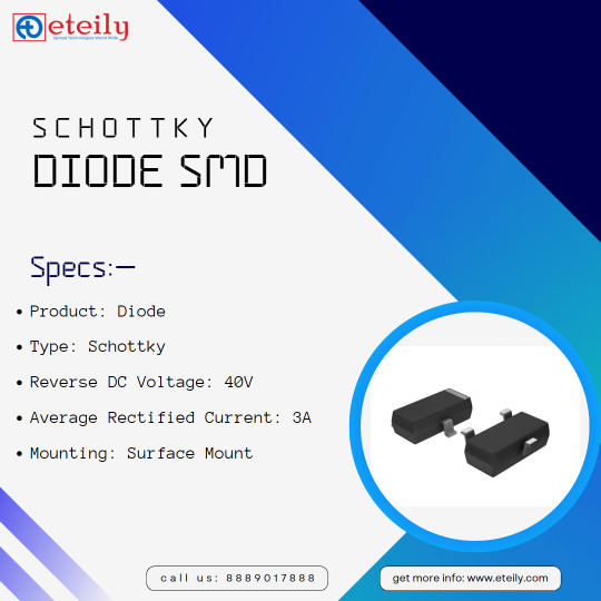
schottky diode smd - PCB Antenna
A diode is a two-terminal electronic component that allows current to flow in one direction while blocking it in the other direction. It is a semiconductor device made up of a p-type material and an n-type material, which are joined together to form a p-n junction.
Diodes are commonly used in electronic circuits for a variety of purposes, such as rectification (converting AC to DC), voltage regulation, and signal modulation. They are also used in power supply circuits, lighting circuits, and electronic displays.
#pcb components#diodes#types of pcb components#types of diodes#pcb components in os#zener diodes#pcb component adhesive#schottky diodes#pcb component assembly#light emitting diodes#pcb component antenna#laser diodes#pcb active components#diodes and transistors#ac pcb components#diodes and triodes#adhesive for pcb components#diodes basics#pcb components buy#"#diodes circuits#pcb board components#diodes cost#pcb basic components#diodes company#pcb buried components#diodes capacitors resistors
0 notes
Text
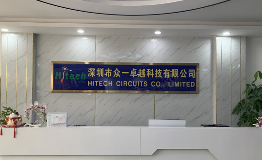
PCB Manufacturing-PCB Assembly-Hitech Circuits
Hitech Circuits is a lеаding PCB Manufacturing & PCB Assembly company with more than 20 years experience in the electronics manufacturing industry. We focus on PCB Design, PCB Layout, Circuit board fabrication, Turnkey PCB assembly, and electronic parts sourcing services.
With mature supply chain, talented design team, advanced manufacturing techniques and quality control systems, Hitech is able to provide one-stop electronics manufacturing services and solution for our customers to help them stand out in the marketplace.
We offer a full range of Electronic manufacturing services.
-LED PCB
-Heavy Copper PCB
-Multilayer PCB
-HDI PCB
-Flexible PCB
-Rigid-Flex PCB
-High Speed PCB
-High Frequency PCB
-PCB Reverse Engineering
7 notes
·
View notes
Text
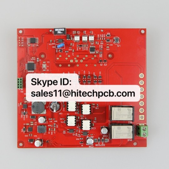
Multilayer SMT Manufacturing PCBA Board
For a Express PCB prototype assembly quote, please email the following files to [email protected] :
BOM list
Gerber files
Quantity required
Our team is qualified to manage the complete process, which includes the sourcing of all components (PCB and Components), online order tracking and their management, PCB assembly, quality control and delivery.
We have specialized experts to deliver fast-turnaround, prototype printed circuit board assembly with surface-mount (SMT), through-hole (THT) and mixed-technology components. Our efficient and express PCBA prototyping service team can assemble printed circuit boards in as little as 24 hours.
5 notes
·
View notes
Text

Components placement is a crucial factor in ensuring optimal performance and reliability in electronic devices. At Shree Ram Electronics, we specialize in precise components placement, leveraging advanced design capabilities and state-of-the-art infrastructure. Our expertise ensures minimal signal interference, efficient heat dissipation, and enhanced circuit efficiency. By focusing on high-quality, cost-effective solutions, we provide end-to-end electronics manufacturing that meets the highest industry standards. With our unparalleled experience, we optimize components placement to deliver innovative and reliable electronic solutions, ensuring superior functionality and durability for our valued customers.
0 notes
Text

We sell —CCTV security systems video Balun from China —-email : [email protected]
#cctv camera#cctvinstallation#china#electronic#video#powersupply#hdmi cable#BNC connector#pcb assembly#audio cable#electronic components#PoE switch#RCA pin jack#RF coaxial connector
0 notes
Text
Explore the commonly used components in PCB assembly, including resistors, capacitors, diodes, and more. Learn how Viasion ensures high-quality assembly for reliable PCBs.
0 notes
Text
Press Fit Connectors: Enabling Reliable and Durable Connections in Electronics Manufacturing

Automating Connections With Press Fit Technology Press connectors provide a simple yet robust method for creating secure electrical connections through automated assembly processes. By utilizing a press or insertion tool, press connectors can be rapidly installed with minimal labor costs compared to traditional wiring methods. This makes them well-suited for high-volume manufacturing environments where quick and reliable connections are essential. Press connectors work by using a mating male and female connection design where the male pin is pressed or inserted into the female housing. The housing features a series of contact beams that flex inward during insertion of the pin. Once the pin is fully seated, the contact beams resiliently grip the pin to hold it securely in place without the need for soldering or crimping. Some key advantages of this press-in joining technology include: - Speed of installation. Press fit connectors can typically be installed in less than a second using automated insertion tools, significantly increasing throughput compared to hand-wiring methods. This reduces assembly time and costs. - Secure, vibration-resistant connections. When fully seated, press fit connections experience contacting pressures of around 40 pounds per square inch, ensuring a tight grip that withstands shock, vibration, and thermal cycling better than loose wire connections. - No heat or complex tooling required. Press Fit Connectorsutilize cold metal-to-metal joining, avoiding the use of soldering irons or crimping tools and heat that could damage sensitive components. Simple automated press tools suffice. - Repeatable connections. The consistent mechanical joining process of press fits provides highly repeatable connections from one unit to the next, improving product quality and reliability compared to hand-wired versions. - Ease of inspection. Fully seated press fit connections are self-locking so visual inspection confirms proper installation. Any missing or loose connections are obvious. - Compatibility with automated assembly. The simple press-in action is easily implemented using pick-and-place robots, conveyor-based presses, or other automated assembly equipment suited to high-volume manufacturing environments. Variations in Press Fit Designs While the general principle of press connectors remains the same, connector manufacturers have developed various innovative designs optimized for different application needs. Some common variations include: - Board-to-board connectors. Often used to make connections between circuit boards stacked vertically in enclosures. Board-to-board press fits feature male pins on one board that press directly into plated-through holes on the mating board below. - Box-header connectors. House receptacles or sockets in an insulating box or header, commonly used for applications like motor controls that need to break out many individual connections. The box speeds assembly and adds grip retention. - Power connectors. Larger press fit connectors may be designed to handle heavier loads like battery connections. Overmolded plastic housings provide strain relief while metal inserts securely join high-current power pins. - Compact right-angle connectors. Useful in space-constrained designs, right-angle press fits allow headers and receptacles to mate vertically instead of inserting straight inline. This saves valuable board area. - Water-resistant connectors. Gaskets and seals incorporated into the connector housing design provide an extra level of protection against moisture ingress for applications demanding an IP rating. Get more insights on Press Fit Connectors
Priya Pandey is a dynamic and passionate editor with over three years of expertise in content editing and proofreading. Holding a bachelor's degree in biotechnology, Priya has a knack for making the content engaging. Her diverse portfolio includes editing documents across different industries, including food and beverages, information and technology, healthcare, chemical and materials, etc. Priya's meticulous attention to detail and commitment to excellence make her an invaluable asset in the world of content creation and refinement.
(LinkedIn- https://www.linkedin.com/in/priya-pandey-8417a8173/)
#Press Fit Connectors#PCB#Electronic Components#Mechanical Assembly#Solderless#Reliability#High Retention Force#Automotive#Aerospace#Telecommunications
0 notes
Text
What are the Key Considerations in Electronic Component Sourcing for Engineering Projects?
Navigate the intricate process of electronic component procurement with insights into stages, factors affecting sourcing, and the debate: in-house design team or Electronics Manufacturing Service (EMS) provider. Uncover strategies to ensure quality, availability, and timely delivery in your projects
#Engineering#Electronic Components#Procurement Strategies#EMS Providers#Quality Assurance#Sourcing Platforms#Project Management#PCB Assembly#Suntronic Inc.
1 note
·
View note
Text
“Like a master conductor leading an orchestra, Avalon Technologies harmonizes design, engineering, and production to create the symphony of electronics manufacturing.”
#electronic manufacturing services#EMS#electronic assembly#PCB manufacturing#electronics design services#electronic component manufacturing#OEM services#electronics production#custom electronics#PCB assembly#electronic engineering services#EMS provider#electronic product manufacturing#turnkey manufacturing services#electronics supply chain.
0 notes
Text
Sharing a Computer with More Friends
A few months ago I built an I/O expansion board for my homebrew 68030 project with a 4-port serial card to go with it, and got BASIC running for four simultaneous users. It worked, but not as well as I had hoped. I wanted to be able to run two of those serial cards to support 8 total users, but it had proven unstable enough that with just the one card I had to slow down the whole system to 8MHz.
So I designed a new serial card.

I had previously been running this computer without any issues at 32MHz with a mezzanine card with FPU & IDE as well as a video card. The main board by itself can clear 56MHz. Having to go all the way down to 8MHz just didn't sit well with me. I want this machine to run as fast as possible for its 8 users.
I put extra time into reviewing worst-case timing for all components and graphing out how signals would propagate. The 16C554 quad UARTs I'm designing around are modern parts that can handle pretty fast bus speeds themselves — easily up to 50MHz with no wait states on the 68030 bus — assuming all the glue logic can get out of the way fast enough.
Signal propagation delays add up quickly.
My first draft schematic used discrete 74-series logic for chip selection, signal decoding, timing, etc. At slower bus speeds this wouldn't have been a problem. But I want this thing to run as fast as possible. By the time critical signals had made it through all those logic gates, I was looking at already being well into one wait state by the time the UART would see a 50MHz bus cycle begin.
I needed something faster. I was also running low on space on the board for all the components I needed. The obvious answer was programmable logic. I settled on the ATF22V10 as a good compromise of speed, size, availability, and programmability. It's available in DIP with gate delays down to 7ns. Where discrete gates were necessary, I selected the fastest parts I could. The final design I came up with showed a worst case timing that would only need one wait state at 50MHz and none for anything slower.
It ended up being a tight fit, but I was able to make it work on a 4-layer board within the same footprint of my main board, putting some components on the back side. (It may look like a bunch of empty space, but there's actually a lot going on running full RS232 with handshaking for 8 ports).
New problem. I had blown my budget for the project. As much as I love those stacked DE9 connectors, they're expensive. And there's no getting around the $10 pricetag for each of those quad UARTs. Even using parts on-hand where possible, I was looking at a hefty Mouser order.
[jbevren] suggested using ganged RJ45 connectors with the Cisco pinout instead of stacked DE9, to save space & cut costs. [Chartreuse] suggested buffering the TTL serial TX/RX signals to drive the LEDs that are frequently included on PCB-mount RJ45 connectors. Both great ideas. I was able to cut 20% off my parts order and add some nice diagnostic lights to the design.
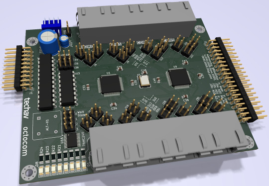
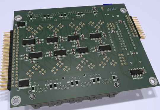
Two weeks later, I received five new PCBs straight from China. I of course wasted no time setting into starting to assemble one.
I really set myself up for a challenge on this one. I learned to solder some 25 years ago and have done countless projects in that time. But I think this might be the most compact, most heavily populated, most surface mount board I've ever assembled myself. (There are 56 size 0805 (that's 2x1.2mm) capacitors alone!)


After a few hours soldering, I had enough assembled to test the first serial port. If the first port worked then the other three on that chip should work too, and there's a great chance the other chip would work as well.

And it did work! After some poking around with the oscilloscope to make sure nothing was amiss, I started up the computer and it ran just fine at 8MHz.
And at 16MHz.
And at 25MHz.
And at 32MHz.
And at 40MHz.
And almost at 50MHz!
Remember what I said about my timing graphs showing one wait state for 50MHz? The computer actually booted up and ran just fine at 50MHz. The problem was when I tried typing in a BASIC program certain letters were getting switched around, and try as I might, BASIC just refused to 'RQN' my program. It was pretty consistently losing bit 3, likely from that signal having to travel just a tiny bit farther than the others. A problem that will probably be resolved with an extra wait state.
Good enough for a first test! A few hours more and I finished assembling the card.

I did have some problems with cleaning up flux off the board, and I had to touch up a few weak solder joints, but so far everything seems to be working. I've updated my little multi-user kernel to run all 8 users from this new card and it's running stable at 40MHz.
I need to update my logic on the 22V10 to fix a bug in the wait state generator. I would love to see this thing actually running at 50MHz — a 25% overclock for the 40MHz CPU I am currently running. I also want to expand my little kernel program to add some new features like the ability to configure the console serial ports and maybe even load programs from disk.
I hope to bring this machine with a collection of terminals and modems this June to VCF Southwest 2025 for an interactive exhibit that can be dialed into from other exhibits at the show.
#wrap030#multi-user BASIC#EhBASIC#homebrew computer#motorola 68030#68030#mc68030#motorola 68k#vcfsw#vcfsw2025#Retrocomputing#rtc#retrotech crew
28 notes
·
View notes
Text
hi,I'm zoe,a sales engineer in the Shenzhen STHL Electronics Co.,Ltd.we are a professional PCB & PCBA manufacturing servicer with more than 18 years of experience located in Shenzhen, China. Mainly provide services of electronic components sourcing + PCB fabrication + PCB Assembly + Housing assembly + Function testing services.
Our factory covers 7000+ square meters, has 5 (Panasonic) high-speed SMT production lines, 2 DIP lines, 2 testing lines, and 180+ workers, passed ISO9001, ISO14001, ISO13485 and IATF 16949 certifications, win recognization by Littelfuse, Hisense,Surfilter, etc.
2 notes
·
View notes
Text
PCB schematic/design/fabrication/assembly
MPN TECH Pte Ltd provides One-Stop PCBA Solutions in Singapore, which support from R&D prototype to mass production. We have built long-term collaborations with many local startups, SIMES, MNCS, etc. We also have lots of overseas PCBA projects in Europe and the US. If any questions feel free to let me know.
Our Solutions:
PCB Design;
PCB Fabrication;
Components souring;
PCB Assembly;(SG Local machine Assembly)
3 notes
·
View notes
Text
HDI PCB & High Interconnect PCB Manufacturing(from Hitech Circuits Co., Limited)
What is a high density PCB board (HDI PCB)?
The HDI board is based on the traditional double panel as the core board, which is made by continuously accumulating. This circuit board made by a continuous layer is also called the Build-Up Multilayer (BUM). Compared with the traditional circuit board, the HDI circuit board has the advantages of "light, thin, short, small".
The electrical connection between HDI's plate layer is achieved by conductive pores, buried holes, and blind holes. Its structure is different from ordinary multi -layer circuit boards. A large number of blind holes are used in HDI boards. HDI PCB uses laser direct drilling, and standard PCB usually uses mechanical drilling, so the number of layers and high width ratio often decreases.
HDI includes the use of fine features or signal traces and spaces of 0.003” (75 µm) or less and laser-drilled blind or buried microvia technology. Microvias allow the use of micro-interconnects from one layer to another within a PCB utilizing a smaller pad diameter creating additional routing density or reducing form factor.
High-density interconnect (HDI) PCBs are characterized by finer lines, closer spaces, and more dense wiring, which allow for a faster connection while reducing the size and bulk of a project. These boards also feature blind and buried vias, laser ablated microvias, sequential lamination, and via in-pads. As a result, a HDI board can house the functionality of the previous boards used. HITECH CIRCUITS is an HDI PCB manufacturer and provider in Shenzhen, China supports HDI PCB prototype and mass production with less expensive price and quick-turn lead time. Customers from a variety of industries we serve have a common that have high expectations in quality, reliability and on-time delivery in HDI PCB production. Our quality is not afterthought, but built into each process from front-end to fabrication and shipping.
HDI PCB's advantages
1. Reduce PCB cost: When the density of PCB increases beyond the eight-layer board, it will be manufactured in HDI, and the cost will be lower than that of traditional complicated press-forming process.
2. Better reliability: Due to the thin thickness and the aspect ratio of 1:1, the micropores have higher reliability when transmitting signals than ordinary through holes.
3. Improves thermal properties: The insulating dielectric material of the HDI board has a higher glass transition temperature (Tg) and therefore has better thermal properties.
4. Improve RF interference / electromagnetic interference / electrostatic discharge (RFI / EMI )
5. Increase design efficiency: Micro-hole technology allows the circuit to be arranged in the inner layer, so that the circuit designer has more design space, so the efficiency of the line design can be higher.
HDI PCB Manufacturing Process
The overall process for manufacturing HDI PCB is essentially the same as for fabricating other PCB board, with notable differences for PCB stack-up and hole drilling. Since HDI boards generally require smaller drill holes for vias, laser drilling is usually required. Although laser drills can produce smaller and more precise holes, they are limited by depth. Therefore, a limited number of layers can be drilled through at a time. For HDI boards, which are invariably multilayer and may contain buried and blind vias, multiple drilling processes may be required. This necessitates successive layer boding to achieve the desired stack-up or sequential lamination cycles. Not surprisingly, this can significantly increase PCB manufacturing time and cost. HDI PCB fabrication is an advanced technology and therefore requires expertise along with specialized equipment like laser drills, laser direct imaging (LDI) capability, and special clean room environments. In order to efficiently manufacture high-quality and reliable HDI PCB products, you must understand the HDI board manufacturing process and coordinate with your HDI PCB supplier to implement good DFM (Design for Manufacturability) for HDI layout design. Therefore, not all board factories have the ability to do the HDI, but Hitechpcb can, we will be here to support our customer needs.
-Consumer Driven Technology
The via - in - pad process supports
More technology on fewer layers, proving that bigger is not always better. Since the late 1980's we have seen video cameras using cartridges the size of a novel, shrink to fit in the palm of your hand. Mobile computing and work at home have further promoted technology to make the computer faster and lighter, allowing consumers to do remote work from anywhere.
HDI technology is the main reason for these changes. The products do more, weigh less, and their bodies are smaller. Professional equipment, mini components and thinner materials reduce the size of electronic equipment, while expanding technology, quality and speed.
-Via in Pad Process
The inspiration from the surface installation technology pushed the restrictions of BGA, COB and CSP to a smaller square surface inch. The via in pad can be placed in the surface of flat land through the cushion process. The via is plated and filled with conductive or non-conductive epoxy resin, and then close and plat it to make it almost invisible.
It sounds simple, but there are eight steps to complete this unique process. Professional equipment and well -trained technicians followed closely to achieve perfect hiding.
-Via Fill Types
There are many different types of via fill materials: non -conductive epoxy, epoxy, copper filling, filling and electrochemical coating. All this leads to via buried in a flat land, and the land will be fully solders as normal land. Vias and mricrovias are drilled, blind or buried, plated, and then hidden under the SMT land. Processing vias of this type of Vias requires special devices and takes time. The process time of multiple drill cycles and controlling deep drills has increased.
-Cost Effective HDI
Although the size of some consumer products is reduced, quality is still the most important factor for consumers. Use HDI technology during the design process, you can reduce the 8-layer through-hole PCB to a 4 layer HDI Microvia technology packed PCB. The elaborate HDI 4-layer PCB wiring function can achieve the same or better functions as standard 8-layer PCB.
Although the Microvia process has increased the cost of HDI PCB, the appropriate design and decrease of layers of counting reduces the cost of the ingredients of the material, and the layer count is large.
-Laser Drill Technology
The smallest micro-vias can provide more technologies on the surface of the plate. Using a beam with a diameter of 20 microns (1 mil), this high impact can be cut through metal and glass to produce tiny via hole. There are new products, such as uniform glass materials, and they are low -loss layer pressure plates and low -dielectric constants. These materials have high heat resistance, can be used for lead -free components, and allows smaller holes.
-Lamination & Materials For HDI PCB Boards
Advanced multilayer technology allows designers to add other layers to form a multilayer PCB. Use laser drills to produce holes in the inner layer, and can be coated when pressed, imaging and etching. The process of this increase is called sequential construction. Hitechpcb HDI PCB manufacturing uses solid -filled VIA can better heat management, connect stronger connection and improve the reliability of the board.
The copper of the resin coating is a assistant with poor pores, with longer drilling time and thinner. Hitechpcb has ultra low contours and ultra thin copper foil, and its surface is fixed on a tiny nodule. This material has chemically treated and started chemical treatment and startup of the most fine and high quality lines and spacing technology.
The dry resistance of the layer pressure plate still uses heating scroll method to apply resistance to core materials. It is now recommended to preheat the material to the required temperature before the layer pressure process of the HDI printing circuit board. The preheating of the material can better apply dry resistance to the surface of the layer pressure plate, pull less calories from the heat roll, and keep the stable export temperature of the layer made products consistent. The consistent entrance and exit temperature cause less air clips under the movie. This is essential for the breeding of fine lines and spacing.
-How difficult is the HDI Printed Circuits Board?
The manufacturing of the HDI PCB (High Denity PCB) is relatively difficult because it needs to use complex manufacturing technique and technology. The following is some difficulties made by HDI PCB:
Multi-layer plate lamination: HDI Printed Circuits Boards are usually composed of multi-layer boards, and multi-layer boards need to be laminated. Multi-layer plates need to control parameters such as temperature, time, pressure to ensure the control quality and thickness control between multi-layer boards.
Blind holes and buried holes: HDI Printed Circuits Boards need to create blind holes and buried holes, which requires technologies such as laser drilling and chemical corrosion to ensure the accuracy and quality of the hole.
Impedance control: HDI Printed Circuit Boards need to control impedance, which requires fine design of the layout and circuit of the circuit board, and uses special materials and processes to achieve impedance control.
Small track space manufacturing: HDI Printed Circuits Boards need to make very small spacing tracks (conductions), which requires high-precision manufacturing equipment and technologies to ensure the accuracy and quality of the circuits.
-The difference between HDI board and normal PCB
The HDI board is generally made of accumulation method. The more times the accumulation layer, the higher the technical grade of the board. Ordinary HDI boards are basically one accumulation. The high-end HDI uses two or more accumulated technologies, and at the same time, advanced PCB technology such as stacked holes, plating filling, and laser direct punching. When the density of PCB increases more than eight layers board, it is made by HDI, and its cost will be lower than the traditional complex compact process.
The electrical performance and signal of the HDI board are higher than that of traditional PCB. In addition, HDI boards have improved better for radio frequency interference, electromagnetic wave interference, electrostatic release, and thermal conduction. High density integration (HDI) technology can make terminal product design more miniaturized, while meeting higher standards for electronic performance and efficiency.
The HDI board uses a blind hole plating to perform secondary pressure, divided into one order, second order, third order, fourth, fifth order, etc. The first order is relatively simple, and the processes and processes are easy to control. The main problem of the second order is the issue of the place, and the other is the problem of punching and copper plating. There are many second order design. One is the wrong position of each order. When connecting the secondary neighborhood, it is connected to the middle layer through the wire. The method is equivalent to two first order HDI. The second is that the two order holes are overlapped. The second -order is realized by the superposition method. The processing is similar to the two first order, but there are many key points of the process. The third type is to punch perforation directly from the outer layer to the third layer (or N-2 layer). There are many different techniques from the front, and the difficulty of punching is even more difficult.
In PCB proofing, HDI costs high, so general PCB proofing manufacturers are unwilling to do it. HITECHPCB can be a HDI Blind PCB board that others are unwilling to do. At this stage, the HDI technology adopted by HITECH has exceeded the highest number of layers of 20 layers; the number of blind holes is 1st to 4th; the minimum pore diameter is 0.076mm, and the process is laser drilling.
HDI PCB Manufacturer & Assembly – One-stop services from China
-HDI (high-density interconnection board) is a compact circuit board designed for small capacity users. Compared with ordinary PCB, the most significant feature of HDI is that the wiring density is high.
HDI PCB Manufacturer & Assembly – One-stop service The HDI PCB is defined as a micro via with a hole diameter of 6 mils or less and a hole diameter of 0.25 mm or less. The contact density is above 130 points/square, and the wiring density is with a line width/pitch of 3 mil/3 mil or less. HDI PCB, the full name is High Density Interconnect PCB, it requires much higher wiring density with finer trace and spacing, smaller vias and higher connection pad density. Blind and buried vias’ design is one of their marked feature. HDI PCB board is widely used in Cell phone, tablet computer, digital camera mother board PCB, GPS, Automobile board, LCD module and other different area.
HDI PCB is the abbreviation for High Density Interconnect PCB or High Density PCB. An HDI PCB is defined as a printed circuit board with a higher wiring density per unit area than a conventional PCB. Hitech Circuits Co., Limited is a professional high density interconnect PCBs, HDI PCB board manufacturer, supplier and design company from China, if you are looking for reliable high density interconnect PCB board partner from China, please don’t hesitate to contact [email protected], from Cynthia.
1 note
·
View note
Text
Precision PCB Soldering Services by Shree Ram Electronics
PCB soldering is a crucial process in electronic manufacturing, ensuring secure and reliable connections for optimal circuit performance. At Shree Ram Electronics, we specialize in high-quality PCB soldering, utilizing advanced techniques to enhance durability and efficiency. Our expertise guarantees precision, minimizing defects while maximizing performance. As a trusted provider of end-to-end electronics solutions, we leverage our unparalleled manufacturing experience, design capabilities, and state-of-the-art infrastructure to deliver cost-effective and innovative soldering services. Whether for small-scale prototypes or large-scale production, we ensure excellence in PCB soldering for all your electronic needs.
0 notes
Text
Selective soldering 🔧🔬🔥
Selective soldering involves attaching specific components to printed circuit boards (PCBs) and molded modules, a method particularly useful for items susceptible to heat damage from standard reflow ovens or wave soldering found in conventional surface-mount technology (SMT) or through-hole assembly techniques. Typically, this method is applied after an initial SMT oven reflow phase. The components targeted for selective soldering are often nestled among others already soldered via a surface-mount reflow method. This demands high precision in the selective soldering process to prevent damage to the surrounding elements.
#adafruit#selectivesoldering#pcbassembly#electronicsmanufacturing#surface-mount#throughhole#reflowprocess#precisionengineering#solderingtechnology#circuitboarddesign#manufacturinginnovation#techadvancements
5 notes
·
View notes
Text
Printed Circuit Board Basics
Most of us are using Printed Circuit Board in our daily life. Printed Circuit Boards are used in almost all the Electronic products, from consumer gadgets such as PCs, tablets, smartphones, and gaming consoles to industrial and even high tech products in strategic and medical electronics domains.
Here, we have some statistics for you that shows how many electronic devices connect worldwide from 2015 to 2025. This statistic shows an increase in the use of a number of PCB in people daily life. Hence, CircuitWala took this opportunity to provide a basic knowledge about PCB via this article.
There are so many books available online which teach about Printed Circuit Board design and hardware part. There are few links available online which shows only a few basic fundamentals of PCB and few are there for Basics of Printed Circuit Board (PCB) Design. Few which gives good know knowledge on Printed Circuit Board terminology. But in the end for the hobbyist, there is no such material available which make their work easy.
Now days there few online designing websites available which allow hobbyist and students to create their design and Printed Circuit Board fabrication part. These websites provide limited features and charge high for the full edition. We, @CircuitWala are in try to provide one platform which provides plenty of Printed Circuit Board knowledge digitally to make your work simple and easy.
Alternatives of PCB include wire wrap and point-to-point construction. Creating a layout of PCB is a little bit time-consuming method as compared to its alternative solution but manufacturing of PCB is cheaper and faster then other wiring methods as electronic components are mounted and wired with one single part.
Let’s start with some basics of Printed Circuit Board with this article. Here in this article we will discuss about history of PCB to understand the emerge of PCB, Types of PCB to make your complex PCB a very simple using different types, Usage of PCB to provide you an idea to create more Printed Circuit Board projects, Advantages and Disadvantages, Possible Future to know about new technological change in Printed Circuit Board manufacturing and also about how to destroy and manage your PCB’s e-waste? We know you are eager to know all the stuff in details but before that let’s make a simple definition of Printed Circuit Board.
What is Printed Circuit Board?Printed Circuit Board is an electronic device made of conductive material(FR-4) like copper which connects components mounted on it to to get desired output by providing an input on another end.
When the board has not mounted with any of the components is called as Printed Circuit Board or Printed Wired Board. Mounting of an electronic component on Printed Circuit Board is called as PCB assembly.
History of Printed Circuit BoardThe invention of Printed Circuit Board was by Austrian engineer Paul Eisler as part of a radio set while working in England around 1936.
In early days before Printed Circuit Board became common in use, Point-to-Point construction was used. This meant some bulky and unreliable design that required plenty of sockets and regular replacement of it. Most of this issue directly address when PCB went into regular production.
Originally, every electronic component had wire leads, and the PCB had holes drilled for each wire of each component. The components’ leads were then passed through the holes and soldered to the PCB trace. This method of assembly is called Through-Hole construction. There is one other method to mount component is called as Surface Mount.
Type of Printed Circuit BoardPCBs are produced from the different types of material and on the basis of that material PCBs are divided mainly into two parts: Rigid PCB and Flexible PCB. Nowadays, a combination of Rigid and flexible PCB is also possible and that is called as Flexi-Rigid PCBs.
Most of the PCBs are built in layers. The inner layer is the base material called as a substrate. Rigid PCBs are mainly made of material like epoxy materials and Flexible PCBs are made of plastic material that can withstand high temperatures.
Rigid PCBs are generally, hard materials that hold the component in a better way. The motherboard in the tower of a computer is the best example of Rigid PCBs. Flexible PCBs fundamental material allows PCB to fit into forms that Rigid PCBs can not. Flexible PCBs can turn round without harmful the circuit on PCB.
All Rigid and Flexible PCBs can come in three formats by layers: Single Layer, Double Layer, and Multi-Layer.
1. Single Layer PCBSingle Layer PCBs have been around since the late 1950s and still dominate the world market in sheer piece volume. Single Sided PCBs contain only one layer of conductive material and are best suited for low-density designs. Single-sided PCBs are easy to design and quick to manufacture. They serve as the most lucrative platform in the industry.
2. Double Layer PCBDouble Layered printed circuit board technology is conceivably the most popular type of PCB in the industry. Double Sided PCB (also known as Double-Sided Plated Thru or DSPT) circuits are the gateway to advanced technology applications. They allow for a closer (and perhaps more) routing traces by alternating between top and bottom layers using vias.
3. Multi Layer PCB
Multilayer PCB is a circuit board that has more than two layers. Unlike a Double-Sided PCB which only has two conductive layers of material, all multilayer PCBs must have at least three layers of conductive material which are buried in the center of the material.
Usage of Printed Circuit BoardBy reading this article till this point, we hope that you are now able to get about printed circuit boards. Now, we will make you understand about different applications of printed Circuit Board.
In this digital world, Printed Circuit Board is in almost all our daily life electronic devices and in our industrial electronics as well. Below are the industries where PCBs are used:
Possible FutureNowadays, most of the circuits are replaced to produce Printed Circuit Board from the old methods. Revolution in technology made many of the processes automated and hence it is easy to manufacture PCB. But still, these processes are a bit expensive to hire, involve toxic waste and use high temperatures and acids. With technological advances we have seen in the past years, it is not hard to imagine PCB will soon be revolutionized. Not only that but research institutes predict a more ‘green’ future for PCBs; PCBs being made of paper.
Electronic Waste (e-waste)Electronic Waste or e-waste is described as discarded electrical or electronic devices. Informal processing of e-waste in developing countries can lead to adverse human health effects and environmental pollution.
Electronic scrap components contain a hazardous substance such as lead, cadmium, beryllium, or brominated flame retardants. Recycling and disposal of e-waste may involve significant risk to health of workers and communities in developed countries and great care must be taken to avoid unsafe exposure in recycling operations
Nowadays, developing countries are encouraging electronic users to take care while recycling the e-waste or submit them to the organization who are involved in such activities.
SummaryIn this blog, we have learned the basics of Printed Circuit Board. CircuitWala is planning to write as many blogs to provide more and more knowledge of Printed Circuit Board. Either it is basics or manufacturing or usages or advantages and disadvantages of PCBs. We will also try to make our users/customers up to date for the new technology innovations, including past histories and revolution of the PCB industries.
In the next blog, we will look at more briefly about the different types of Printed Circuit Board. We also understand the process to make it and different usage and application for the same.
#electronic circuit design company#pcb circuit manufacturer in ahmedabad#pcb design & manufacturing services#printed circuit board companies#printed circuit board order online#PCB manufacturer#Printed Circuited Board#double layer PCB#PCB Quality Control
2 notes
·
View notes