#double layer PCB
Explore tagged Tumblr posts
Visit Tumblr Blog
Explore Tumblr blogs with no restrictions, modern design and the best experience.
Last Seen Tumblr Blogs


Fun Fact
BuzzFeed published a report claiming that Tumblr was utilized as a distribution channel for Russian agents to influence American voting habits during the 2016 presidential election in Feb 2018.
Text
Printed Circuit Board Basics
Most of us are using Printed Circuit Board in our daily life. Printed Circuit Boards are used in almost all the Electronic products, from consumer gadgets such as PCs, tablets, smartphones, and gaming consoles to industrial and even high tech products in strategic and medical electronics domains.
Here, we have some statistics for you that shows how many electronic devices connect worldwide from 2015 to 2025. This statistic shows an increase in the use of a number of PCB in people daily life. Hence, CircuitWala took this opportunity to provide a basic knowledge about PCB via this article.
There are so many books available online which teach about Printed Circuit Board design and hardware part. There are few links available online which shows only a few basic fundamentals of PCB and few are there for Basics of Printed Circuit Board (PCB) Design. Few which gives good know knowledge on Printed Circuit Board terminology. But in the end for the hobbyist, there is no such material available which make their work easy.
Now days there few online designing websites available which allow hobbyist and students to create their design and Printed Circuit Board fabrication part. These websites provide limited features and charge high for the full edition. We, @CircuitWala are in try to provide one platform which provides plenty of Printed Circuit Board knowledge digitally to make your work simple and easy.
Alternatives of PCB include wire wrap and point-to-point construction. Creating a layout of PCB is a little bit time-consuming method as compared to its alternative solution but manufacturing of PCB is cheaper and faster then other wiring methods as electronic components are mounted and wired with one single part.
Let’s start with some basics of Printed Circuit Board with this article. Here in this article we will discuss about history of PCB to understand the emerge of PCB, Types of PCB to make your complex PCB a very simple using different types, Usage of PCB to provide you an idea to create more Printed Circuit Board projects, Advantages and Disadvantages, Possible Future to know about new technological change in Printed Circuit Board manufacturing and also about how to destroy and manage your PCB’s e-waste? We know you are eager to know all the stuff in details but before that let’s make a simple definition of Printed Circuit Board.
What is Printed Circuit Board?Printed Circuit Board is an electronic device made of conductive material(FR-4) like copper which connects components mounted on it to to get desired output by providing an input on another end.
When the board has not mounted with any of the components is called as Printed Circuit Board or Printed Wired Board. Mounting of an electronic component on Printed Circuit Board is called as PCB assembly.
History of Printed Circuit BoardThe invention of Printed Circuit Board was by Austrian engineer Paul Eisler as part of a radio set while working in England around 1936.
In early days before Printed Circuit Board became common in use, Point-to-Point construction was used. This meant some bulky and unreliable design that required plenty of sockets and regular replacement of it. Most of this issue directly address when PCB went into regular production.
Originally, every electronic component had wire leads, and the PCB had holes drilled for each wire of each component. The components’ leads were then passed through the holes and soldered to the PCB trace. This method of assembly is called Through-Hole construction. There is one other method to mount component is called as Surface Mount.
Type of Printed Circuit BoardPCBs are produced from the different types of material and on the basis of that material PCBs are divided mainly into two parts: Rigid PCB and Flexible PCB. Nowadays, a combination of Rigid and flexible PCB is also possible and that is called as Flexi-Rigid PCBs.
Most of the PCBs are built in layers. The inner layer is the base material called as a substrate. Rigid PCBs are mainly made of material like epoxy materials and Flexible PCBs are made of plastic material that can withstand high temperatures.
Rigid PCBs are generally, hard materials that hold the component in a better way. The motherboard in the tower of a computer is the best example of Rigid PCBs. Flexible PCBs fundamental material allows PCB to fit into forms that Rigid PCBs can not. Flexible PCBs can turn round without harmful the circuit on PCB.
All Rigid and Flexible PCBs can come in three formats by layers: Single Layer, Double Layer, and Multi-Layer.
1. Single Layer PCBSingle Layer PCBs have been around since the late 1950s and still dominate the world market in sheer piece volume. Single Sided PCBs contain only one layer of conductive material and are best suited for low-density designs. Single-sided PCBs are easy to design and quick to manufacture. They serve as the most lucrative platform in the industry.
2. Double Layer PCBDouble Layered printed circuit board technology is conceivably the most popular type of PCB in the industry. Double Sided PCB (also known as Double-Sided Plated Thru or DSPT) circuits are the gateway to advanced technology applications. They allow for a closer (and perhaps more) routing traces by alternating between top and bottom layers using vias.
3. Multi Layer PCB
Multilayer PCB is a circuit board that has more than two layers. Unlike a Double-Sided PCB which only has two conductive layers of material, all multilayer PCBs must have at least three layers of conductive material which are buried in the center of the material.
Usage of Printed Circuit BoardBy reading this article till this point, we hope that you are now able to get about printed circuit boards. Now, we will make you understand about different applications of printed Circuit Board.
In this digital world, Printed Circuit Board is in almost all our daily life electronic devices and in our industrial electronics as well. Below are the industries where PCBs are used:
Possible FutureNowadays, most of the circuits are replaced to produce Printed Circuit Board from the old methods. Revolution in technology made many of the processes automated and hence it is easy to manufacture PCB. But still, these processes are a bit expensive to hire, involve toxic waste and use high temperatures and acids. With technological advances we have seen in the past years, it is not hard to imagine PCB will soon be revolutionized. Not only that but research institutes predict a more ‘green’ future for PCBs; PCBs being made of paper.
Electronic Waste (e-waste)Electronic Waste or e-waste is described as discarded electrical or electronic devices. Informal processing of e-waste in developing countries can lead to adverse human health effects and environmental pollution.
Electronic scrap components contain a hazardous substance such as lead, cadmium, beryllium, or brominated flame retardants. Recycling and disposal of e-waste may involve significant risk to health of workers and communities in developed countries and great care must be taken to avoid unsafe exposure in recycling operations
Nowadays, developing countries are encouraging electronic users to take care while recycling the e-waste or submit them to the organization who are involved in such activities.
SummaryIn this blog, we have learned the basics of Printed Circuit Board. CircuitWala is planning to write as many blogs to provide more and more knowledge of Printed Circuit Board. Either it is basics or manufacturing or usages or advantages and disadvantages of PCBs. We will also try to make our users/customers up to date for the new technology innovations, including past histories and revolution of the PCB industries.
In the next blog, we will look at more briefly about the different types of Printed Circuit Board. We also understand the process to make it and different usage and application for the same.
#electronic circuit design company#pcb circuit manufacturer in ahmedabad#pcb design & manufacturing services#printed circuit board companies#printed circuit board order online#PCB manufacturer#Printed Circuited Board#double layer PCB#PCB Quality Control
2 notes
·
View notes
Text
Understanding Circuit Board Electronic Components: A Comprehensive Guide
In today's digital world, electronic devices have become an essential part of our daily lives. But what makes these devices tick? At the heart of every electronic device lies a circuit board—a masterpiece of tiny electronic components working together to perform complex tasks. In this article, we’ll dive deep into the fascinating world of circuit board electronic components, exploring each element’s role and how they contribute to the overall functionality of the device.
What is a Circuit Board?
A circuit board, often referred to as a PCB (Printed Circuit Board), is a flat board used to mechanically support and electrically connect various electronic components. These components work in unison to perform a specific task. Think of the circuit board as the skeleton and nervous system of an electronic device—it holds everything together and allows communication between parts.
Types of Circuit Boards
Single-sided PCB: Has one layer of conducting material.
Double-sided PCB: Contains two layers for components and connections.
Multi-layer PCB: Complex boards with multiple layers for advanced applications.
The Role of Electronic Components on a Circuit Board
Every electronic device you interact with is powered by a carefully designed circuit board filled with various components. These components might be tiny, but each one has a critical role in the operation of the device. Here's a breakdown of the most important electronic components you’ll find on a typical circuit board.
1. Resistors
Resistors are fundamental components that control the flow of electrical current. They resist the flow of electrons, hence the name "resistor." Their primary function is to reduce current flow, adjust signal levels, and divide voltages in a circuit. Without resistors, circuits would allow too much current to flow, potentially damaging other components.
Types of Resistors
Fixed resistors: Have a set resistance value.
Variable resistors: Allow adjustment of the resistance.
2. Capacitors
Capacitors store and release electrical energy in a circuit. They are often compared to small rechargeable batteries that quickly charge and discharge. Capacitors help smooth out fluctuations in voltage, filter noise, and store energy for future use.
Common Uses of Capacitors
Energy storage
Signal filtering
Voltage stabilization
3. Inductors
Inductors are components that store energy in a magnetic field when electrical current flows through them. They resist changes in current and are typically used in circuits to filter signals, manage power, and store energy.
Applications of Inductors
Power supplies
Radio frequency circuits
Noise suppression in circuits
4. Diodes
A diode is like a one-way valve for electricity, allowing current to flow in only one direction. They are vital in circuits to prevent reverse currents, which can damage components.
Types of Diodes
Light-emitting diodes (LEDs): Produce light when current flows through.
Zener diodes: Regulate voltage within a circuit.
5. Transistors
The transistor is a versatile component used to amplify or switch electronic signals. In essence, transistors are like tiny switches that turn signals on and off rapidly, making them essential in modern electronics.
Types of Transistors
NPN transistors: Allow current flow when a small voltage is applied to the base.
PNP transistors: Conduct when the base is negatively charged.
How Circuit Board Components Work Together
In a circuit, each component has a specific role, and together they form a cohesive system. For example:
Capacitors and resistors may work together to filter signals or smooth out voltage fluctuations.
Transistors and diodes ensure that signals are amplified or directed properly.
Integrated circuits handle the complex tasks, processing data, and controlling the overall system.
Choosing the Right Components for Your Circuit Board
When designing or repairing a circuit board, choosing the correct components is crucial. Some factors to consider include:
Voltage requirements
Power consumption
Signal type and frequency
Physical size and compatibility
Conclusion
Circuit boards are an integral part of any electronic device. The various components on the board each play a specific role in ensuring the device functions as intended. Understanding these components, from resistors to integrated circuits, is essential for anyone working with electronics, whether you're designing a new system or troubleshooting an existing one.
2 notes
·
View notes
Text
Wrap030-ATX Says "Hellorld"

In the immortal word of [Usagi Electric], Wrap030-ATX says, "Hellorld". This can only mean one thing — serial I/O is working!
Getting serial working should be relatively straightforward. The UART I'm using is an 8-bit peripheral which needs a Chip Enable and an Output Enable signal, just like the ROM. It's a little slower, so it will need an extra wait state or two, but it should be easy enough to modify the bus controller state machine to address the UART as well. It didn't take me long to add the necessary logic, solder on the new parts, and fire it up for a test run.
Nothing happened.
I went through all the normal steps — double check the wiring, make sure my test leads haven't come loose, make sure the chip is seated properly in its socket and not shorted out …
… I burned my finger. And not just a little 'ow that's a bit warm to the touch', but a proper second-degree burn. That UART chip was hot.
That kind of heat can only mean there is a direct short somewhere in the chip. It could just be a defective part, but since they are out of production and I only have a few on hand, the best thing to do is confirm the problem isn't on my board somewhere before trying another one (and potentially destroying it too).
The PCB layout passed Design Rule Check, so I didn't have any overlapping traces. The schematic didn't have any obvious errors where maybe I had inadvertently tied an output signal to power or ground. This was not an existing library part — it was one that I had to create — so it was possible I had gotten pin assignments wrong.
I pulled up the datasheet and opened the part in the library and started confirming all of the pin assignments matched the datasheet. Bus & I/O pins were all fine; but the very last power supply pin was assigned to Vcc, where the datasheet had it marked Vss. So I had a +5V power supply capable of sourcing in excess of 25A of current running into what should have been a ground pin. No wonder it was hot enough to burn; it's a wonder it didn't release the magic smoke immediately.
This is a challenge. I need to swap a power pin for a ground pin on a PLCC socket. On a simpler project, I might've gotten away with just cutting the trace running to that pin and soldering a bodge wire to it.
… But this is a 4-layer board. There is no mere trace running to that pin — there is an entire inner layer attached to it. My best bet would probably be removing the offending pin from the socket, but depending on how it's constructed, I may not be able to remove the pin.
Through-hole PLCC socket pins are staggered. Some go straight down through the board, but alternating pins make an L-shape so that the socket can have two rows of through-hole pins at a 0.1" grid spacing. The L-shaped pins would be trapped under the plastic base of the socket.
Luckily, the pin in question was the first on its side, so it went straight through the base. I started by bending up its contact, and then with the heat turned up on my soldering iron, I was able to pull it out of the board and completely free from the socket.
I had some wire on hand that was just the right width to match the slots for the contacts in the socket. I bent a flat loop to make contact with the chip lead and shoved it down into the slot. It worked perfectly. I ran it over to a nearby jumper that had a ground lead, and there I have my first bodge wire for this project.
It still didn't work.
This is the part of debugging that is the most frustrating. There's a problem and it takes a considerable amount of effort to identify not just the cause, but also the solution. And then after working through those steps and finally implementing a fix, it still doesn't work because there is another problem. Back to square 1 with debugging.
Why is it not working? It's not burning hot, so that problem was indeed solved. I'm getting data to the chip, and the read/write strobes are functional. The chip select signals are ... wait, why isn't chip select working?
... Because I forgot a chip, that's why. Insert Picard facepalm GIF here.
The UART I'm using is a Western Digital WD16C552. It's a lovely chip designed for 386 era PCs contain two 16550-compatible UARTs and a Centronics Parallel port as well. It is three peripherals in one package. To save I/O on my bus controller CPLD, I used a 74'139 2-to-4 decoder to further break down the address for this serial/parallel I/O chip into the three specific peripheral select signals I needed. And I simply forgot to solder that chip onto the board.
Two headers and one 74LS139 later and finally my terminal came to life. The Wrap030-ATX whispered its very first greeting, "HELLORLD". Serial I/O is working and I can move on to the next step. And oddly enough, I tested that first chip that flirted with fire and it actually still works!
I am racing forward through the countless tests and steps to bring this machine to life ahead of VCF Southwest at the end of June. I am hoping to get it at least running BASIC over serial by that time, but for that I am going to need some RAM. This will be fun because this is my first time actually building a DRAM controller; I've done some test designs before but never actually built them. Fingers crossed I don't run into any show-stopping errors getting it up and running.
#homebrew computing#mc68030#motorola#motorola 68k#motorola 68030#vintage computing#vcf southwest#wrap030 atx#western digital
21 notes
·
View notes
Text

Aluminium PCB
Aluminium PCB are metal-based, copper-clad laminates with a good heat dissipation function. Usually, Aluminium PCB is refer to LED PCB board, which is the most important part of LED display and lighting products, etc.
Hitech Circuits Co., Limited is a professional aluminum pcb board, LED PCB manufacturer in China. Through 10 years of aluminum pcb board designing and manufacturing experience, Hitech are able to provide high quality and cost effective single layer, double layer and multi layer aluminum pcb boards to global customers. For any of your requirements regarding aluminum pcb board, please don’t hesitate to contact [email protected]
#Aluminium PCB#aluminum pcb#pcb assembly#pcb#engineering#technology#pcba#pcb manufacturer#pcbassembly#pcb design#hardware
5 notes
·
View notes
Text
Multilayer PCBs (Printed Circuit Boards) offer numerous advantages over their single-layer or double-layer counterparts. These benefits arise from their enhanced design capabilities, improved performance, and greater flexibility. Here are some key advantages of multilayer PCBs:
#PCB#printed circuit board manufacturers#electronic cable assembly#pcb manufacturing#pcb assembly manufacturer#pcb assembly services#pcb board manufacturer#printed circuit board manufacturer in india#circuit board manufacturing#pcb exporters#pcba#pcb manufacturer#pcb design#pcbassembly#multilayer pcb
2 notes
·
View notes
Text
another new toy


I've been planning to get a number of accessories for my new computer. A new monitor, microphone, maybe one of those vr headsets. But after having it for a few weeks, one thing jumped out as needing an upgrade more urgently than anything else - the stock full size keyboard that came with it was just too large and awkward for my little keyboard shelf. I was tempted to go back to the Microsoft Compact Bluetooth keyboard that I was using with the Steam Deck... but I haven't had a "real" computer, like a proper desktop computer in decades, I wanted a "real" keyboard to go with it. Like a proper mechanical keyboard with switches and buttons and such. And so I typed "mechanical keyboard reviews" into a youtube search, blissfully unaware of the rabbit hole I was about to fall down.
If you know then you already know, but it came as a surprise to me that membrane keyboards are so cheap and so easy to mass produce that they've taken over the casual market altogether, forcing mechanical keyboards into the domain of the ⋆ ˚。⋆˚enthusiast⋆ ˚。⋆˚
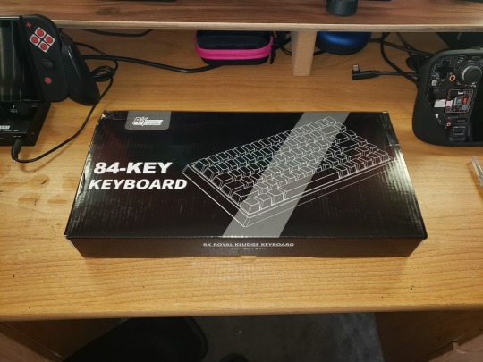
Yes, it seems proper keyboards are a hobby now, not a very cheap one either, and the very last thing I need is another expensive hobby. But every hobby has its more affordable and approachable on ramps, and there are a number of pre-built budget boards occupying this space in world of mechanical keyboards. After watching a few dozen hours of youtube videos and reading a bunch of reviews and tutorials, I eventually settled on the RK84 'limited edition' from Royal Kludge for us$80. Which is like twice what I expected to pay when I in my naive innocence began shopping for keyboards, but I've come to understand that eighty bucks absolutely counts as "budget" in this hobby.
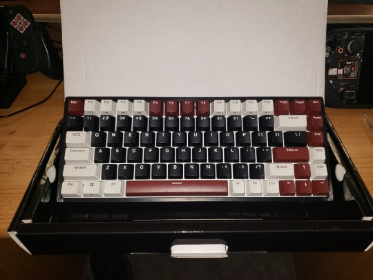
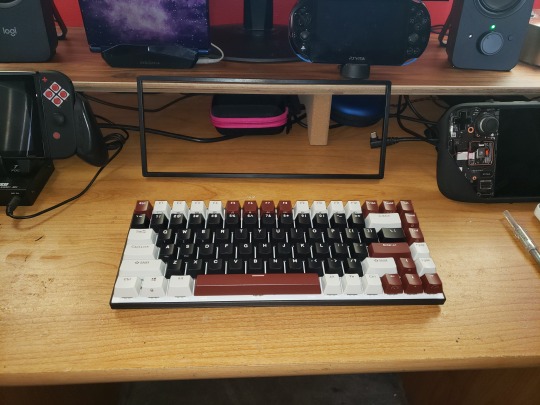
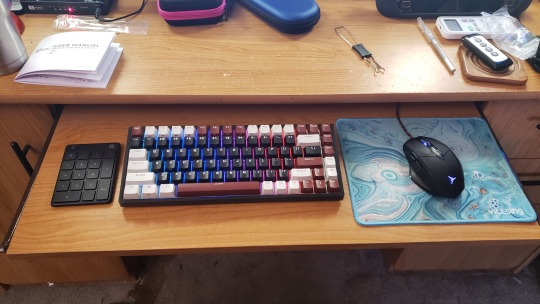
Pricing aside, I really do love my new keyboard. The 75% form factor is ideal, better centering the typing keys and saving a bunch of extra space on my little shelf while maintaining all the functionality of a full size board save only for the number pad. While I do like to use a number pad, I don't mind taking one out when I need it, and the keyboard even has a couple usb ports to easily plug a mouse and separate number pad into, which is super convenient and such an obvious idea that I really have to wonder why all keyboards aren't doubling as USB multi-dongles at this point, with additional usb ports, sd card ports, and so on.
For $10 more than the regular RK84 wireless, the 'limited edition' version has better keycaps, factory-lubed switches, some filler foam in the housing to reduce the hollow sound, an additional layer of sound dampening foam sandwiched between the top plate and the pcb, and a snazzy color scheme, the version I chose combining a black body and mostly black keys with a white top plate that better reflects the swirly rainbow rgb backlighting. The sound is decent, at least to my untrained ear, right out of the box. Which is ideal, as I'd like to avoid the temptation to start modding it.
Because I've gone about as far down this particular rabbit hole as I want to go.
Though I suppose it is tempting to open it up, as some basic tape & band aid mods would be cheap and easy and might improve the sound a bit...
And as much as the pre-lubed yellow linear switches are nice, I did make sure to get a hot-swappable board so it's easy to change them out later if I want to try alternatives, and I do think I might prefer tactile switches for typing...
And the rgb lighting is nice enough that it really is a shame these caps aren't shine though. Yeah, yeah, shine-through is tacky, but Cringe is Dead, and some black top pudding caps might really make the lighting pop. Or maybe a mix of black, white and some accent color to match the color layout that the board came with?
The abyss, it tempts me so...
#mechanical keyboard#keyboards#computers#I really can't be starting any expensive new hobbies#student loan payments start back up in September
3 notes
·
View notes
Text
Exploring Multilayer PCBs: The Backbone of Modern Electronics
Introduction In the world of electronics, Multilayer Printed Circuit Boards (PCBs) serve as essential components that enable compact and efficient designs. These innovative boards have become a cornerstone of modern technology, used in everything from consumer gadgets to industrial equipment. In this article, we'll explore the structure, advantages, and applications of multilayer PCBs.Get more news about Multilayer PCB,you can vist our website!
What Are Multilayer PCBs? Multilayer PCBs consist of multiple layers of conductive material stacked together, separated by insulating layers called dielectric materials. The layers are interconnected through vias, small holes filled with conductive material, allowing signals to travel between them. Unlike single or double-layer PCBs, multilayer designs can include three or more layers, making them suitable for complex circuits requiring higher functionality.
Advantages of Multilayer PCBs
Compact Size: By stacking layers, multilayer PCBs minimize the size of the final electronic product. This is crucial for devices like smartphones and wearables, where space is at a premium.
Enhanced Performance: With multiple layers, these PCBs offer superior electrical properties, such as reduced electromagnetic interference (EMI) and improved signal integrity.
Durability: The lamination process used in their production provides robust mechanical strength and thermal reliability.
Increased Functionality: The extra layers allow for more complex circuit designs, making them ideal for high-performance applications.
Applications of Multilayer PCBs Multilayer PCBs are found across a variety of industries, including:
Consumer Electronics: Smartphones, tablets, and laptops all rely on multilayer PCBs for their advanced functionality.
Automotive Industry: Modern vehicles incorporate these boards for sensors, entertainment systems, and engine control units.
Medical Devices: From imaging systems to life-support machines, multilayer PCBs enable precise and reliable operation.
Telecommunications: Routers, switches, and other network equipment depend on multilayer boards for signal processing and connectivity.
Manufacturing Challenges While multilayer PCBs offer numerous benefits, their production is not without challenges. The manufacturing process requires advanced techniques, such as precise layer alignment and reliable via drilling. Quality control is critical to ensure functionality, especially as the number of layers increases.
Conclusion Multilayer PCBs are indispensable in today’s technological landscape, offering the ideal combination of size, performance, and functionality. As industries continue to demand more advanced electronic devices, the role of multilayer PCBs is set to grow even further. Their innovative design and versatility highlight their importance as a backbone of modern electronics.
0 notes
Text
Top Microwave PCB Manufacturer for High-Quality RF Microwave PCB Fabrication
ASC-I is a leading microwave PCB manufacturer, specializing in the design and microwave PCB fabrication of high-performance RF microwave PCBs. Our microwave PCBs are engineered for precision, durability, and superior signal integrity, making them ideal for industries such as aerospace, defense, telecommunications, medical, and automotive. With advanced manufacturing techniques and high-frequency materials, we ensure that every RF microwave PCB meets the highest standards of quality and reliability.

Why Choose ASC-I for Microwave PCB Fabrication?
1. Expert Microwave PCB Manufacturer with Proven Industry Experience
With years of expertise, ASC-I delivers cutting-edge microwave PCB fabrication solutions. Our team of engineers and technicians specializes in producing high-frequency RF microwave PCBs that offer minimal signal loss and exceptional thermal stability.
2. High-Performance Materials for Microwave PCBs
We use advanced laminates like Rogers, Teflon, and ceramic-filled PTFE in our microwave PCB fabrication process. These materials provide low dielectric loss, high-frequency stability, and superior thermal resistance, ensuring optimal performance for microwave PCBs in demanding environments.
3. Custom RF Microwave PCB Solutions for Complex Applications
ASC-I offers customized RF microwave PCB solutions to meet specific requirements. Whether you need single-layer, double-layer, or multilayer microwave PCBs, we provide tailored designs with precise impedance control and optimized performance.
4. Advanced Manufacturing & Rigorous Testing
As a trusted microwave PCB manufacturer, we follow strict quality control protocols. Our microwave PCB fabrication process includes signal integrity analysis, impedance verification, and environmental testing to ensure that every RF microwave PCB meets industry standards for reliability and efficiency.
Applications of Microwave PCBs
Our microwave PCBs are designed for high-frequency applications across multiple industries, including:
Aerospace & Defense: Radar systems, satellite communication, avionics, and military-grade RF technology.
Telecommunications: 5G base stations, RF transceivers, and high-speed wireless communication.
Medical Technology: MRI, CT scanners, and RF-based diagnostic systems.
Automotive & IoT: ADAS (Advanced Driver Assistance Systems), vehicle-to-vehicle communication, and IoT applications.
ASC-I: Your Trusted Partner for Microwave PCB Fabrication
As a premier microwave PCB manufacturer, ASC-I is committed to delivering high-quality RF microwave PCBs with industry-leading performance. Our microwave PCB fabrication expertise, combined with cutting-edge technology and stringent quality control, ensures that we provide the best microwave PCBs for your specific applications.
If you need reliable, high-performance RF microwave PCBs, ASC-I is the perfect choice. Contact us today to discuss your microwave PCB fabrication requirements and experience top-tier manufacturing solutions.
0 notes
Text

Flexible PCB Manufacturing
What is Flex PCB?
Flexible printed circuits, also known as flex circuits, are sometimes regarded as a printed circuit board (PCB) that can bend, when in reality there are significant differences between PCB’s and flex circuits when it comes to design, fabrication and functionality. One common mistake that designers make is to design a flexible circuit using the same rules as a PCB. Flex PCB require a unique set-up and have their own set of design rules that the Hitechpcb team has termed “flex-izing” and have worked hard to perfect over the last many years.
Flexible PCB, which also called Flex PCB, Flexible circuit board or flex circuit, it consists of PI base material, adhesive layer, copper layer, coverlay and sometimes with stiffeners. Flexible PCBs are now being used widely to replace traditional FR4 PCB in various different applications due to the benefits from flex PCB specially. Although more expensive than a normal rigid PCB, the right design in the right application could save weight and time in assembly, coupled with the reliability which makes flexible circuit board a worthwhile consideration.
A flexible printed circuit consists of a metallic layer of traces, usually copper, bonded to a dielectric layer, usually polyimide. Thickness of the metal layer can be very thin (<.0001″) to very thick (> .010″) and the dielectric thickness can vary from .0005″ to .010″. Often an adhesive is used to bond the metal to the substrate, but other types of bonding such as vapor deposition can be used to attach the metal.
How to calculate your flex pcb bend radius?
Because copper tends to readily oxidize, the exposed surfaces are often covered with a protective layer, gold or solder are the two most common materials because of their conductivity and environmental durability. For non-contact areas a dielectric material is used to protect the circuitry from oxidation or electrical shorting.
The number of material combinations that could go into a flexible printed circuit are nearly endless; current, capacitance, chemical and mechanical resistance, temperature extremes and type of flexing are just some of the criteria that impacts the material selections that best meet the functional needs. An experienced Hitechpcb design engineer takes the critical requirements into consideration when designing a circuit to meet your needs.
Flexible printed circuit boards (FPC) has become a common component of electronic products due to its lightness and flexibility performance. It is widely used in smart terminal, wearable electronics, consumer, automotive, industrial and medical fields. The miniaturization and integrated function of electronics product development is driving FPC to fine line and multilayer design.
What is Multilayer flex PCB?
This type of flexible printed wiring boards are multilayered (with three or more conductor layers) and require plated-through holes. We could use through vias, buried vias and blind vias.
A multi layer flex circuit combine several single-sided or double-sided circuits with complex interconnections, shielding and/or surface mounted technologies in a multi layer design. The multi layers may or may not be continuously laminated together throughout the production process. If your design needs require maximum flexibility, continuous lamination may not be appropriate. Multi layer circuits are an effective solution when confronted with design challenges such as: unavoidable crossovers, specific impedance requirements, elimination of crosstalk, additional shielding and high component density. You can also link here to learn more about flex pcb bending radius.
Benefits to Flex PCB including:
Assembly Error Reduction
Decreased Assembly Time and Costs
Design Freedom
Flexibility during Installation
High Density Applications
Improved Airflow
Increased Heat Dissipation
Increased System Reliability
Point-to-Point Wire Replacement
Reliability and Durability
Repeatable Routings
Simplified Circuit Geometry
Package Size and Weight Reduction
Flex PCB Static Application
An application where flexible circuits are flexed only to install the circuit and fit it into its application (also known as flex-to-fit or flex-to-install). A static application will typically be made using the less expensive Electro Deposited (ED) copper.
Flex PCB Dynamic Flexing Applications
A situation where the flexible circuit itself is dynamically (repeatedly) flexed during the actual use of the final product. Common examples include flip-type cell phones, laptops, printer heads and robotic arms. A dynamic application will require the use of Rolled Annealed (RA) copper.
High Density Flex PCB Applications
Flexible circuits allow for minutely narrow lines giving way to high density device population. Denser device populations and lighter conductors can be designed into a product, freeing space for additional product features.
With a large number of investments on the facilities of flexible printed circuit board and continuously innovating the flexible circuit board manufacturing technology, Hitech Circuits is able to manufacture flexible PCBs with a great variety of technologies, from simple single sided flex PCB, double sided flex PCB to complex multilayer flexible PCB, Rigid flex pcb and support prototype FPC with laser cutting & flying probe test to mass production with toolings.
Multilayer flex PCB bookbinding
Circuit bookbinding is one of the best practices employed by Hitechpcb engineers for creating stacked PCBs. For flex PCBs, we offered a 12 layer flex PCB board with bookbinding. An additional small length is added to the circuit, making it move in an outward direction from the bend radius. There are copper traces placed at right angles to the bend. This helps restrict the circuit bend in one direction.
The length to be added depends on total number of layers in the PCB, as well as the tightness of the bend. The advantage of circuit bookbinding is that it removes a great amount of tension from the various circuit layers during the bending process. The method also helps prevent buckling of the circuits at the exact bend radius.
The bookbinded PCBs can easily meet the tight tolerance requirements in comparison to bonded PCBs. This is why this 12 layer flex PCB is a perfect choice for applications where stricter tolerances are required. Its polyamide construction delivers immense strength and flexibility. This flexi PCB can easily perform 180° bends. Also, the construction helps prevent buckling of inner layers, which often occurs in a long term use. This flexibility also helps reduce stress on the internal components. This 12 layer flex PCB board has better shelf life than a 12 layer bonded circuit board. The immersion gold plating offers low contact resistance, good wetting, as well as excellent shelf life. We can provide the 12 layer flex PCB board with book binding in width 4/4 mil, with minimum finish thickness 0.15 mm flex and maximum 1.6 mm.
Advantages of Flexible PCB
Flexible PCB technology often has a wide range of possibilities for different designs and products.
The flexible feature is among the best attributes of the cables, wires, connectors and even PCBs.
Some of the advantages of using the flexible circuit include:
Reduces the overall weight and size.
A flex circuit can reduce the weight of a device by up to 70%.
Improves the packaging of electronics
It gives you the ability to solve interconnect and packaging issues as it can bend, form and move.
Interconnect solution as it reduces the amount of interconnects such as cables, wires, pcbs and connectors.
Conformability as the slender nature of the material allows for making of 3D packages
Electrical integration – You can easily come up with custom solutions basing your design on a plethora of choices of materials. Apart from that, you have the freedom to choose from the myriad of designs and plating procedures.
Heat dissipation ability or power – The polyimide dielectric has the ability to withstand very high temperatures. You can, therefore, use it for high power applications.
Electrical and mechanical repeatability
Cost saving as you can save up to 30% of the total cost of hand wiring and other assembly processes.
You can also save on space by almost 30%
It is more reliable as it does not have any wiring errors
Despite the numerous advantages, the flexible PCB also has its disadvantages.
Let’s have a look.
Disadvantages of Flexible PCB
Every electronic solution must have certain demerits.
Some of the disadvantages include:
Flexible PCB
A higher initial cost – Since the flex circuit is often custom for particular electronics. The initial cost of designing, photographic plate and layout is very high. This limits you to using it on large quantities to save on cost.
Flexible circuit repairs and changes are very difficult – The initial process is not just expensive but difficult to come up with. Once you have the base map, it becomes difficult to make any more changes. Removing and replacing the covering film for repair is also extremely difficult.
It is often small in size – The batch process of making the flexible circuits often limits the size of the flexible circuit. The production equipment limits you from making wider and longer sizes.
Easy to damage – Improper personal operations can easily damage the flexible circuits. Rework and soldering will require the expertise of a technician.
The process of assembly is also very difficult.
Do not let the disadvantages kill your spirits.
Why Not Make All Circuit Boards Flexible?
Flexible circuit boards are certainly useful, but they are not going to replace rigid circuit boards for all applications. Cost efficiency is the main obstacle to implementing an exclusively flexible circuit board design in a consumer product. Rigid circuit boards are less expensive to manufacture and install in a typical automated high-volume fabricating facility.
Typically, the ideal solution for an innovative product is one that incorporates flexible circuitry when necessary and employs solid, reliable rigid circuit boards where possible to keep manufacturing and assembly costs down.
Some manufacturers even use hybrid rigid-flex printed circuit boards expressly for this purpose. This is common in laptop computers and medical devices, where rigid circuit boards can be connected to one other using ribbon-like flexible circuits. These boards can be compounded and designed to meet any number of engineering needs by focusing on the respective strengths of each circuit board base technology.
Hitech Circuits creates both flexible and printed circuit boards for product manufacturers. Enjoy a consultation with one of our sales reps to find out if your product prototype design is best served by flexible or rigid circuit board types.
What is Flexible PCB and Its Production Process?
Flexible PCB (Flexible Printed Circuit, FPC) is very popular with excellent characteristics such as low weight and thin thickness, etc. It is also can be folded freely. Flexible PCB mainly relies on manual visual inspection with high cost and low efficiency. With the rapid development of the electronics industry, the design of printed circuit board has become more and more high -precision and high- density, traditional manual testing methods can no longer meet production needs. FPC defect automation testing has become an inevitable trend of industrial development.
Flexible printed circuit (FPC) is a technology developed by theUnited Statesto develop aerospace rocket technology in the 1970s. It is high reliability, excellent deflection made by polyester film or polyimide as a substrate material. A flexible circuit is formed by embedding a circuit design in a thin, flexible plastic sheet that is flexible, allowing a large number of precision components to be stacked in a narrow and limited space. This circuit can be bent and folded at will. Flexible has the characteristics like light weight, small size, good heat dissipation, easy installation, etc, it breaks through the traditional interconnection technology in the structure of the flexible circuit, the material is composed of insulating film conductor and adhesive
Flexible PCB includes single sided FPC, double sided FPC and multilayer FPC, etc. Single FPC has chemically etched conductive pattern layer, the conductive pattern layer on the surface of the flexible insulating substrate is calendered copper foil. The insulating substrate may be polyimide, polyethylene terephthalate, arylamide fiber ester and polyvinyl chloride. The double sided FPC on both sides of the insulating base has a conductive graphics made of etching, which increases the wiring density of the unit area. Metal hole connects the graphic connection on both sides of the insulation material to form a conductive pathway to meet the flexible design and function. The covering film can protect the single, double -sided wire and indicate the position of the component placed. According to demand, metal holes and coverage layers are optional. This type of Flexible PCB has fewer applications. Multi -layer flexible PCB is to press the single-sided or double-sided flexible circuit layer of 3 or more layers together. The metal hole is formed by drilling and electroplating, and conductive channels are formed among different layers. In this way, there is no need to use a complex welding process. Multi-layer circuits have huge functional differences in higher reliability, better thermal conductivity and more convenient assembly performance.
At present, the production process of flexible PCB mainly includes looping, Sizing conductor, etching, routing of the conductors, ground planes, sizing of the holes, filleting, button plating, adhesive-backed films, screen-print liquid overcoats, photo imaginable liquid, film polymers and other processes. See the figure for the specific production process.
0 notes
Text
Printed Circuit Board (PCB) Market Resilience and Risk Factors Impacting Growth to 2033
Introduction
Printed Circuit Boards (PCBs) are an integral component of modern electronics, providing the foundation for the operation of nearly all electronic devices. The growing demand for consumer electronics, industrial automation, medical devices, and automotive electronics has led to significant growth in the PCB industry. This article explores the latest trends, market dynamics, and forecast for the PCB industry from 2024 to 2032.
Market Overview
The global PCB market is expected to witness steady growth over the forecast period, driven by increasing demand for high-performance electronic components and advancements in PCB manufacturing technologies. The market size, valued at approximately USD XX billion in 2023, is projected to reach USD XX billion by 2032, growing at a CAGR of XX% during the forecast period.
Download a Free Sample Report:-https://tinyurl.com/pxzydt82
Key Market Drivers
1. Rising Demand for Consumer Electronics
The proliferation of smartphones, tablets, wearables, and other consumer electronic devices has significantly contributed to the expansion of the PCB market. With innovations such as 5G connectivity, foldable displays, and smart home devices, PCBs with higher reliability and density are required.
2. Growth in Automotive Electronics
The automotive industry is increasingly incorporating advanced electronic systems, such as ADAS (Advanced Driver Assistance Systems), infotainment systems, and electric vehicle (EV) battery management systems. These require high-performance PCBs to ensure efficient operation.
3. Increasing Adoption of IoT and AI Technologies
The adoption of IoT (Internet of Things) and AI (Artificial Intelligence) in industrial, healthcare, and consumer applications is driving the need for sophisticated PCB designs. IoT devices require compact, multi-layer PCBs with enhanced connectivity features.
4. Expansion in Industrial Automation
Industries are investing in automation, robotics, and smart manufacturing, all of which rely on robust PCBs for seamless functionality. The rise of Industry 4.0 and digital transformation initiatives have propelled the demand for high-quality PCB solutions.
5. Advancements in PCB Manufacturing Technologies
Innovations such as flexible PCBs, rigid-flex PCBs, and HDI (High-Density Interconnect) PCBs have enhanced performance and enabled miniaturization. Advanced materials such as polyimide and ceramic substrates have improved thermal and electrical properties, making PCBs more reliable and efficient.
Market Segmentation
The PCB market can be segmented based on type, substrate, application, and region.
By Type:
Single-Sided PCBs
Double-Sided PCBs
Multi-Layer PCBs
Rigid PCBs
Flexible PCBs
Rigid-Flex PCBs
HDI PCBs
By Substrate:
FR-4 (Flame Retardant)
Metal-based PCBs (Aluminum, Copper, etc.)
Ceramic-based PCBs
By Application:
Consumer Electronics (Smartphones, Wearables, Laptops, etc.)
Automotive (ADAS, EVs, Battery Management Systems, etc.)
Industrial (Automation, Robotics, Smart Factories)
Healthcare (Medical Devices, Wearable Health Monitors, Imaging Systems)
Telecommunications (5G Infrastructure, Data Centers, Network Equipment)
By Region:
North America (U.S., Canada, Mexico)
Europe (Germany, UK, France, Italy, etc.)
Asia-Pacific (China, Japan, South Korea, India, etc.)
Latin America
Middle East & Africa
Regional Insights
Asia-Pacific: The Largest Market
Asia-Pacific dominates the global PCB market, with China leading in PCB production due to its large electronics manufacturing sector, cost-effective labor, and advanced fabrication technologies. Countries like South Korea, Japan, and Taiwan also play crucial roles in high-tech PCB manufacturing.
North America: Technological Advancements
North America is witnessing growth due to investments in advanced PCB technologies, particularly in sectors like aerospace, defense, and telecommunications.
Europe: Rising Demand for Automotive Electronics
With strong automotive and industrial manufacturing bases, Germany and France are key players in Europe's PCB market.
Emerging Trends
1. Miniaturization and High-Density Interconnects (HDI)
As devices become more compact, HDI PCBs with finer line widths and higher component density are gaining traction.
2. Flexible and Wearable PCBs
Flexible PCBs are crucial for wearable technology, medical implants, and foldable smartphones.
3. Eco-Friendly PCBs
Sustainable PCB manufacturing using lead-free soldering, bio-degradable substrates, and reduced chemical waste is becoming a priority.
4. 5G and High-Frequency PCBs
With the rollout of 5G networks, PCBs that support high-speed signal transmission and low latency are in demand.
5. AI and Automation in PCB Manufacturing
AI-driven automated optical inspection (AOI) and robotic assembly lines are improving PCB quality and production efficiency.
Challenges in the PCB Industry
Supply Chain Disruptions: Fluctuations in the availability of raw materials, such as copper and laminates, impact production.
Environmental Regulations: Stricter environmental laws demand sustainable manufacturing practices.
High Initial Investment Costs: Advanced PCB manufacturing requires significant capital investment.
Geopolitical Risks: Trade restrictions and geopolitical tensions can affect PCB supply chains.
Future Outlook
The PCB industry is poised for steady growth, with technological advancements shaping the future of electronics. Smart manufacturing, AI-driven design, and green PCB initiatives will drive market evolution. Companies investing in R&D, automation, and sustainable practices will maintain a competitive edge.
Conclusion
The PCB market is witnessing transformative changes driven by advancements in technology and increasing demand across multiple industries. While challenges like supply chain constraints and regulatory requirements persist, opportunities in automotive, healthcare, and telecommunications are expected to fuel the industry's expansion. The forecast for 2032 presents a promising landscape for PCB manufacturers, suppliers, and stakeholders worldwide.
Read Full Report:-https://www.uniprismmarketresearch.com/verticals/semiconductor-electronics/printed-circuit-board-pcb
0 notes
Text
What Makes Flexible PCB Different in PCB Board Fabrication?
In the world of PCB board fabrication, the advancement of circuit boards has driven to the improvement of flexible PCBs, advertising noteworthy points of interest over conventional rigid PCBs. A flexible PCB, as the title proposes, is outlined to twist, bend, and acclimate to different shapes, making it perfect for advanced compact and high-performance electronic gadgets. PCB Fabrication Manufacturer have received inventive methods to deliver these flexible circuits, guaranteeing solidness, unwavering quality, and effectiveness. This article investigates the key contrasts that set flexible PCBs separated in the PCB board fabrication process.
1. Fabric Composition
One of the most basic contrasts between flexible PCBs and rigid PCBs lies in their fabric composition. Not at all like rigid PCBs, which utilize fibreglass-based substrates such as FR4, flexible PCBs are made utilizing high-performance plastic substrates like polyimide or polyester movies. These materials give flexibility, warm resistance, and great electrical cover, making them reasonable for applications where twisting and energetic developments are required.
2. Plan and Auxiliary Differences
PCB Board Fabrication for flexible circuits requires a diverse plan approach. Whereas rigid PCBs have settled layers with copper follows on strong substrates, flexible PCBs utilize lean and flexible copper thwart that can withstand rehashed flexing. The plan prepare moreover includes optimizing follow formats to avoid stretch breaks due to twisting. PCB fabrication Manufacturers utilize progressed methods like laser boring and exact carving to guarantee tall exactness in making perplexing circuit designs on flexible substrates.
3. Manufacturing Techniques
The manufacturing prepare for flexible PCBs varies altogether from that of rigid PCBs. Since flexible PCBs need the mechanical back of rigid boards, extraordinary taking care of procedures are required to avoid harm amid PCB board fabrication. Strategies such as roll-to-roll handling are commonly utilized to deliver flexible circuits effectively. Furthermore, flexible PCBs frequently join single-layer, double-layer, or multilayer plans, depending on the application requirements.
4. Assembly and Component Placement
Component assembly in Flexible PCB presents special challenges. Not at all like rigid PCBs, which give a steady stage for component situation, flexible PCBs require cautious dealing with amid Assembly to maintain a strategic distance from avoid deformation. PCB fabrication Manufacturers utilize specialized cements and patching methods, such as anisotropic conductive film (ACF) holding and flexible patch veils, to guarantee dependable associations without compromising the board’s flexibility.

5. Warm Administration and Reliability
Flexible PCBs offer predominant warm execution due to their lightweight and heat-resistant materials. Polyimide substrates, in specific, can withstand tall temperatures, making them appropriate for applications in cruel situations. Additionally, flexible PCBs dispense with the require for bulky connectors and wiring, decreasing the chances of mechanical disappointments and moving forward by and large unwavering quality in energetic applications like wearable innovation and car electronics.
6. Applications and Advantages
Flexible PCBs are broadly utilized in restorative gadgets, aviation, car frameworks, and customer gadgets due to their space-saving and lightweight properties. Their capacity to adjust to non-standard shapes makes them fundamental in present day compact contraptions like savvy phones, keen observes, and flexible shows. Furthermore, they decrease Assembly complexity, upgrade flag judgment, and make strides strength, making them a favoured choice for high-performance applications.
Conclusion
Flexible PCBs stand out in PCB board fabrication due to their special fabric properties, imaginative fabricating procedures, and flexible applications. PCB manufacture Manufacturers proceed to refine their forms to meet the developing request for flexible circuits in progressed gadgets. As innovation advances, flexible PCBs are set to revolutionize the hardware industry, empowering unused conceivable outcomes in plan and usefulness.
0 notes
Text
Industrial Electronic Repairs Ltd (IER) specializes in the repair of industrial Printed Circuit Boards (PCBs), offering services for single-layer, double-sided, and multi-layer PCBs. Recognizing that sourcing replacements can be challenging due to obsolescence or high costs, IER provides a reliable and cost-effective alternative. Utilizing advanced component testing technology, their experienced engineers diagnose and repair thousands of PCBs annually, addressing issues such as faulty components, burnt-out tracks, and software anomalies. They also offer reprogramming of integrated circuits and, when necessary, can remanufacture obsolete PCBs in low quantities. All in-house repairs come with a two-year warranty, ensuring quality and peace of mind.
1 note
·
View note
Text
A Comprehensive Guide to Printed Circuit Board (PCB) Manufacturing
Title: A Comprehensive Guide to Printed Circuit Board (PCB) Manufacturing
Introduction Printed Circuit Boards (PCBs) are the backbone of modern electronic devices, providing a platform for electrical connections between components. The manufacturing process of PCBs requires precision, technical expertise, and adherence to industry standards to ensure high functionality and reliability. This guide will walk you through the PCB manufacturing process, covering essential topics, strategies, and step-by-step tutorials.
Outline
Overview of PCB Manufacturing
Importance of PCBs in modern electronics
Types of PCBs (Single-layer, double-layer, multi-layer, rigid, flexible, rigid-flex) pcb assembly
Common materials used in PCB fabrication
PCB Design and Layout
Introduction to PCB design software (Eagle, Altium, KiCad, OrCAD)
Key design considerations (trace width, spacing, via placement)
Design for manufacturability (DFM) guidelines
Prototyping and testing the design before manufacturing
PCB Fabrication Process
Substrate material selection
Copper cladding and etching process
Layer alignment and lamination in multilayer boards
Drilling and plating through-holes and vias
Component Assembly and Soldering Techniques
Surface Mount Technology (SMT) vs. Through-Hole Technology (THT)
Pick-and-place machines and manual component placement
Reflow soldering and wave soldering processes
Inspection methods (Automated Optical Inspection, X-ray, Functional Testing)
Quality Control and Testing Strategies
Electrical testing (Flying probe, bed-of-nails testing)
Environmental stress testing (thermal cycling, humidity testing)
Common defects and troubleshooting techniques
Tutorials for DIY and Small-Scale PCB Manufacturing
How to create a PCB at home using etching techniques
Using a CNC machine for PCB prototyping
Ordering PCBs from a professional manufacturer (Gerber file preparation and submission)
Future Trends in PCB Manufacturing
Advances in flexible and stretchable PCBs
3D printed circuit boards
AI-driven PCB design and automated manufacturing
Conclusion The PCB manufacturing process is a blend of design, engineering, and precise execution. Understanding the various steps, from design to assembly and testing, helps ensure the production of high-quality and reliable PCBs. With advancing technology, the industry continues to evolve, offering more efficient and sophisticated solutions. Whether you're a hobbyist, an engineer, or a manufacturer, mastering PCB manufacturing techniques is essential for innovation in electronics.
By following the strategies and tutorials outlined in this guide, you can confidently design and manufacture PCBs that meet your specific requirements.
0 notes
Text
A Comprehensive Guide to Printed Circuit Board (PCB) Manufacturing
Introduction Printed Circuit Boards (PCBs) are the backbone of modern electronic devices, providing a platform for electrical connections between components. The manufacturing process of PCBs requires precision, technical expertise, and adherence to industry standards to ensure high functionality and reliability. This guide will walk you through the PCB manufacturing process, covering essential topics, strategies, and step-by-step tutorials.
Outline
Overview of PCB Manufacturing
Importance of PCBs in modern electronics pcb assembly
Types of PCBs (Single-layer, double-layer, multi-layer, rigid, flexible, rigid-flex)
Common materials used in PCB fabrication
PCB Design and Layout
Introduction to PCB design software (Eagle, Altium, KiCad, OrCAD)
Key design considerations (trace width, spacing, via placement)
Design for manufacturability (DFM) guidelines
Prototyping and testing the design before manufacturing
PCB Fabrication Process
Substrate material selection
Copper cladding and etching process
Layer alignment and lamination in multilayer boards
Drilling and plating through-holes and vias
Component Assembly and Soldering Techniques
Surface Mount Technology (SMT) vs. Through-Hole Technology (THT)
Pick-and-place machines and manual component placement
Reflow soldering and wave soldering processes
Inspection methods (Automated Optical Inspection, X-ray, Functional Testing) pcb manufacturing
Quality Control and Testing Strategies
Electrical testing (Flying probe, bed-of-nails testing)
Environmental stress testing (thermal cycling, humidity testing)
Common defects and troubleshooting techniques
Tutorials for DIY and Small-Scale PCB Manufacturing
How to create a PCB at home using etching techniques
Using a CNC machine for PCB prototyping
Ordering PCBs from a professional manufacturer (Gerber file preparation and submission)
Future Trends in PCB Manufacturing
Advances in flexible and stretchable PCBs
3D printed circuit boards
AI-driven PCB design and automated manufacturing
Conclusion The PCB manufacturing process is a blend of design, engineering, and precise execution. Understanding the various steps, from design to assembly and testing, helps ensure the production of high-quality and reliable PCBs. With advancing technology, the industry continues to evolve, offering more efficient and sophisticated solutions. Whether you're a hobbyist, an engineer, or a manufacturer, mastering PCB manufacturing techniques is essential for innovation in electronics.
By following the strategies and tutorials outlined in this guide, you can confidently design and manufacture PCBs that meet your specific requirements.
0 notes
Text
Rigid Circuits: An Overview
Rigid circuits are a fundamental component of modern electronic devices, widely used across industries such as telecommunications, consumer electronics, automotive, and aerospace. These circuits are made using rigid materials as their base substrate, providing mechanical stability and durability. This article explores the key characteristics, advantages, and applications of rigid circuits, providing a comprehensive understanding of their significance in electronics manufacturing.
What are Rigid Circuits? Rigid circuits are printed circuit boards (PCBs) fabricated on solid and inflexible substrates. Unlike flexible or hybrid PCBs, rigid circuits maintain their shape and cannot be bent or flexed. Key features of rigid circuits include:
Electrical Insulation: Excellent dielectric properties ensure effective insulation between conductive layers.
Mechanical Strength: High tensile strength and durability, suitable for multilayer and high-density designs.
Thermal Resistance: Can withstand elevated temperatures, making them suitable for heat-intensive applications.
Longevity: Designed for long-term reliability in various environments.
Advantages of Rigid Circuits
Structural Stability: Rigid circuits provide a robust framework that protects components from physical stress and mechanical damage.
Cost-Effectiveness: The manufacturing processes for rigid PCBs are well-established, allowing for efficient mass production at a reasonable cost.
Versatility: Compatible with a variety of designs, including single-sided, double-sided, and multilayer configurations.
Enhanced Performance: Rigid circuits offer stable performance in high-speed and high-power applications.
Applications of Rigid Circuits
Consumer Electronics: Used in smartphones, tablets, laptops, and other devices for compact and efficient designs.
Telecommunications: Found in routers, network equipment, and signal transmission systems due to their reliable electrical properties.
Automotive: Essential for engine control units, infotainment systems, and advanced driver-assistance systems (ADAS).
Aerospace and Defense: Trusted for avionics, radar systems, and other critical equipment due to their durability and reliability.
Industrial Equipment: Incorporated in control panels, robotics, and precision machinery for high-performance operations.
Limitations of Rigid Circuits While rigid circuits are versatile and reliable, they have certain limitations:
Lack of Flexibility: Rigid circuits cannot be bent or shaped to fit unconventional enclosures, limiting their use in some applications.
Weight: Heavier compared to flexible PCBs, which may be a disadvantage in weight-sensitive designs.
Thermal Challenges: Although thermally resistant, advanced heat dissipation requirements may require additional cooling solutions or alternative materials.
Conclusion Rigid circuits are a cornerstone of the electronics industry, offering durability, reliability, and high performance across a range of applications. Their robust design and adaptability make them a preferred choice for countless industries. However, as technology progresses, alternative circuit types like flexible and rigid-flex PCBs may complement or replace traditional rigid circuits in specific use cases.
0 notes
Text
How to identify multilayer pcb?
Multilayer printed circuit boards and double-sided PCB boards are similar in appearance. Ordinary people can’t see the difference between them without paying attention, or you can’t tell whether it is a double-sided PCB board or multilayer PCB board. So, how to distinguish between ordinary double-sided PCB boards and multi-layer PCB boards?
First of all, we must have an understanding of the number of layers of the circuit board. The number of layers of the PCB board is the inner layer. 1 layer is referred to as single layer PCB, and 2 layers is referred to as double sided PCB. Multilayer PCB board refers to 4-48 layers; the higher the number of layers, the higher the unit price. Because the inner layer of the circuit is to be pressed, the technical content is high, and the machine cost is relatively high.
Generally speaking, you can identify multilayer pcb by following:
The more layers, the larger the shadow in the sheet;
Dim shadows can be seen in the multi-layer PCB circuit board, if the shadow is light then you can see a little dim, and if the shadow is deep you can see the circuit clearly;
Multilayer PCB circuit boards generally have a smooth surface, especially when they are cleaned after forming and processing;
If you want to know how many layers of the PCB board are, and the precise data, you can only check through the IM inspection of the manufacturer or the PCB drawing of the development engineer.

0 notes