#diodes and triodes
Explore tagged Tumblr posts
Visit Tumblr Blog
Explore Tumblr blogs with no restrictions, modern design and the best experience.
Last Seen Tumblr Blogs


Fun Fact
Tumblr has 4 main sources of revenue.
Text
the graybles eps r so funny just for cuber. if you thought adventure time slang was weird NOW wait until language has changed over ANOTHER thousand years. actually he might just be an alien idk.
#CATCH YOU ON THE TRIODE FLIPPIN THE DIODE or whatever the fuck he said#Literally nigh on incomprehensible#basilposting#atlb
2 notes
·
View notes
Text
youtube
Why The First Computers Were Made Out Of Light Bulbs
0 notes
Text
1950’S TRANSISTOR TRAINING FILM " SEMI-CONDUCTORS: DIODE AND TRIODE FUN...
youtube
0 notes
Text
Best Capacitors manufacturer in India

Electronic component:
An electronic component is any basic discrete electronic device or physical entity part of an electronic system used to affect electrons or their associated fields. Electronic components are mostly industrial products, available in a singular form and are not to be confused with electrical elements, which are conceptual abstractions representing idealized electronic components and elements. A datasheet for an electronic component is a technical document that provides detailed information about the component’s specifications, characteristics, and performance.
Advantages of Electronic components:
These leads connect to other electrical components, often over wire, to create an electronic circuit with a particular function (for example an amplifier, radio receiver, or oscillator). Basic electronic components may be packaged discretely, as arrays or networks of like components, or integrated inside of packages such as semiconductor integrated circuits, hybrid integrated circuits, or thick film devices. The following list of electronic components focuses on the discrete version of these components, treating such packages as components in their own right.
Classification Electronic components:
Active components rely on a source of energy (usually from the DC circuit, which we have chosen to ignore) and usually can inject power into a circuit, though this is not part of the definition.[1] Active components include amplifying components such as transistors, triode vacuum tubes (valves), and tunnel diodes.
Passive components cannot introduce net energy into the circuit. They also cannot rely on a source of power, except for what is available from the (AC) circuit they are connected to. As a consequence, they cannot amplify (increase the power of a signal), although they may increase a voltage or current (such as is done by a transformer or resonant circuit). Passive components include two-terminal components such as resistors, capacitors, inductors, and transformers.

Electromechanical components can carry out electrical operations by using moving parts or by using electrical connections.
Most passive components with more than two terminals can be described in terms of two-port parameters that satisfy the principle of reciprocity — though there are rare exceptions.[2] In contrast, active components (with more than two terminals) generally lack that property.
Explore our wide range of resistor options designed to meet your electronic component needs. Discover SMD resistors and DIP resistors, available in various power ratings and resistance values, providing versatile solutions for circuit designs.
Additionally, we offer Ceramic Varactors for applications requiring variable capacitance. For higher power applications, our Wire Wound Resistors provide excellent performance and durability. Looking for light-dependent resistors (LDRs) We have those too!
For bulk production, we offer SMD resistor reels, providing convenience and efficiency in large-scale manufacturing. Browse our selection and find the perfect resistors for your electronic projects.
Electronic components like Resistors, Capacitors, Inductors, semiconductor ICs, Relays form the backbone of all the technological advances today. With these, you can design any system, any model for your project.
As the saying goes “You want it, we got it” and we at robu take extra pride in providing the highest quality products to fulfill your ideas at the best price.
All products are shipped within 24 hours and delivered right to your doorstep with the minimum shipping charges.
Film resistors are essential components in electronic circuits, offering precise resistance values. Browse our comprehensive selection of film resistors, including carbon film and metal film variants, renowned for their stability and reliability. Explore various wattages, tolerances, and sizes suitable for diverse applications, from basic circuits to intricate electronic projects.
With exceptional temperature stability and low noise performance, our film resistors ensure optimal functionality in your designs. Whether you’re a hobbyist or a seasoned engineer, find the perfect film resistors to meet your requirements and elevate your projects.
Trust in our quality offerings for dependable performance and seamless integration into your circuits.
1 note
·
View note
Text

Component description of PCBA patch processing
PCBA patch processing mainly includes two major processes: PCB circuit board production and SMT patch processing. Electronic components are indispensable in the process. Electronic components are the basic part of PCBA patch processing and an important factor affecting the performance and quality of PCBA finished products. So what are the commonly used electronic components for PCBA patch processing?
1. Resistor
Resistors are electronic components with resistance characteristics and are one of the most widely used components in PCBA processing. Resistors are divided into fixed resistors and variable resistors (potentiometers), which play the role of voltage division, current division and current limiting in the circuit.
2. Capacitors
Capacitors are also one of the basic components in PCBA processing. They are components that store electrical energy and play the role of coupling, filtering, DC isolation and tuning in electronic circuits.
3. Inductor coils
Inductor coils are referred to as inductors and have the function of storing magnetic energy. Inductor coils are usually composed of skeletons, windings, shielding covers, magnetic cores, etc.
4. Potentiometers
Resistors with variable resistance values, that is, resistors that can be continuously adjusted within a specified range, are called potentiometers. The potentiometer consists of a housing, a sliding end, a rotating shaft, a ring resistor and three lead-out terminals.
5. Transformer
The transformer consists of an iron core (or magnetic core) and a coil. The coil has two or more windings, of which the winding connected to the power supply is called the primary coil, and the remaining windings are called the secondary coil.
The transformer is a device that converts voltage, current and impedance. When an AC current flows through the primary coil, an AC magnetic flux is generated in the iron core (or magnetic core), causing a voltage (or current) to be induced in the secondary coil. The transformer is mainly used for AC voltage conversion, current conversion, power transmission, impedance conversion and buffer isolation, etc. It is one of the indispensable important components in the PCBA machine.
6. Crystal diode
The crystal diode (i.e. semiconductor diode, hereinafter referred to as diode) is made of a PN junction, electrode leads and an external sealed tube shell, and it has a unidirectional conductive characteristic.
7. Crystal triode
The crystal triode (hereinafter referred to as triode) is the core device for signal amplification and processing, and is widely used in PCBA machines.
8. Field Effect Transistor
Field effect transistor (FET for short) is also a semiconductor device with PN junction. Unlike triode, it does not use the conductive property of PN junction, but its insulating property.
9. Electroacoustic Device
The device used to complete the conversion between electrical signal and sound signal in the circuit is called electroacoustic device. There are many types of it, including speakers, microphones, headphones (or earplugs), transmitters, receivers, etc.
10. Photoelectric Device
Photoconductive devices that work with the photosensitive properties of semiconductors, photovoltaic cells and semiconductor light-emitting devices that work with semiconductor photovoltaics are collectively referred to as photoelectric devices.
11. Display Device
Electronic display device refers to a photoelectric conversion device that converts electrical signals into optical signals, that is, a device used to display numbers, symbols, text or images. It is a key component of electronic display devices and has a great impact on the performance of display devices.
12. Sensor
The sensor can sense the specified measured value and convert it into a usable signal according to a certain rule. It is usually composed of a sensitive element and a conversion element.
13. Surface Mount Components
Surface mount components (SMC and SMD) are also called patch components or chip components. They include resistors, capacitors, inductors and semiconductor devices, etc. They have the characteristics of small size, light weight, no leads or very short leads, high installation density, high reliability, good vibration resistance, and easy automation.
14. Thyristor
SCR, short for silicon-controlled rectifier, is a high-power semiconductor device with a four-layer structure of three PN junctions, also known as thyristor. It has the characteristics of small size, relatively simple structure and strong functions, and is one of the more commonly used semiconductor devices.
15. Switches, relays, and various connectors
Switches are used to cut off, connect or convert circuits in electronic equipment. Relays are automatic control devices that will change the output in a jumpy manner when the input quantity (electricity, magnetism, sound, light, heat) reaches a certain value.
If you have interest in our service, please feel freely contact Cynthia at [email protected] & 86 18126197150.
0 notes
Text
SMT production process

Program the SMT placement machine
According to the BOM position map provided by the customer, program the coordinates of the location of the components. Then carry out the first piece with the SMT chip processing data provided by the customer.
Printing solder paste
The solder paste is stenciled to the PCB board where the electronic component SMD needs to be soldered to prepare for the soldering of the components. The equipment used is a screen printing machine (printing machine), which is located at the forefront of the SMT chip processing production line.
SPI
Solder paste detector, detects whether the solder paste printing is a good product, whether there is less tin, leaking tin, more tin and other undesirable phenomena.
4.SMT
Accurately install the electronic components SMD on the fixed position of the PCB. The equipment used is a placement machine, which is located behind the screen printing machine in the SMT production line.
The placement machine is divided into high-speed machine and general-purpose machine.
High-speed machine: used to paste components with large pin spacing and small pin spacing
Universal machine: paste small pin pitch (pin density), bulky components.
High temperature solder paste melting
Mainly, the solder paste is melted at high temperature, and after cooling, the electronic components SMD and the PCB board are firmly welded together. The equipment used is a reflow soldering furnace, which is located behind the placement machine in the SMT production line.
AOI
Automatic optical detector to detect whether the soldered PCBA components have poor soldering, such as tombstone, displacement, empty soldering, etc.
Visual inspection
The key items of manual inspection and inspection: whether the PCBA version is the changed version; whether the customer requires components to use substitute materials or components of designated brands and brands; IC, diodes, triodes, tantalum capacitors, aluminum capacitors, switches, etc. Whether the direction of the directional components is correct; defects after welding: short circuit, open circuit, fake parts, fake welding.
Packaging
Products that have passed the test will be packaged separately. The commonly used packaging materials are anti-static bubble bags, electrostatic cotton, and blister trays. There are two main packaging methods, one is to use anti-static bubble bags or electrostatic cotton into rolls, which are the most commonly used packaging methods at present; the other is to customize blister trays according to the size of PCBA. Put it in a blister tray and unpack it, mainly for PCBA boards that are sensitive and have vulnerable patch components.
0 notes
Text
Watch "As Foxconn-Vedanta deal snaps, a look at semiconductors & 'design giant' India’s 40-yr chip struggle" on YouTube
youtube
In layman's term a semiconductor has minaturised huge electronic ckts. These electronic ckt were earlier made of glass tubes called triodes and diodes out of which logical ckt were made and a single blow of any tube would stall the whole system
The triode got replaced with transistors but still occupied space ,with the advent of semiconductors ,the physical space occupied by a single transistor on printed circuit board, now can be filled with millions of transistors.This is the magic of semiconductors which brought about miniturisation
Moreover These electronic ckts were not robust,they consumed lot of electricity,and space.
With the invention of semiconductors, computing power has increased million folds a smart phone has more computing power which can easily fit in your poket than an earlier Main frame computers which occupied 1000 's sq foot area earlier.
Nano technology is packing more logical ckts on the earlier version of semiconductor with size remaining the same or even getting minaturised further.
THIS IS HOW YOU SHOULD EXPLAIN.A JOURNALIST LIKE U SHOULD CONSULT SOME EXPERT ,RATHER THAN SPEAK IN A CONFUSED WAY.
You waisted many minutes

Mohalli was the wrong choice ...for SCL
0 notes
Text
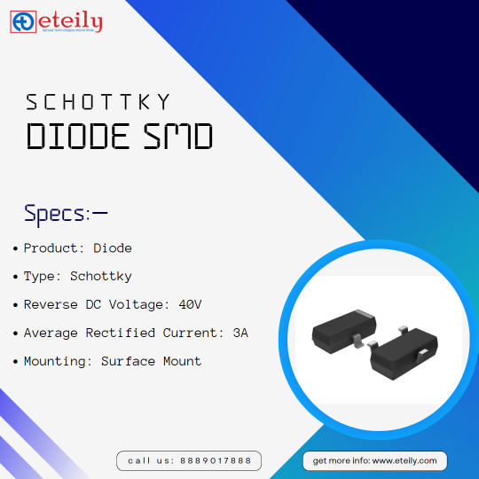
schottky diode smd - PCB Antenna
A diode is a two-terminal electronic component that allows current to flow in one direction while blocking it in the other direction. It is a semiconductor device made up of a p-type material and an n-type material, which are joined together to form a p-n junction.
Diodes are commonly used in electronic circuits for a variety of purposes, such as rectification (converting AC to DC), voltage regulation, and signal modulation. They are also used in power supply circuits, lighting circuits, and electronic displays.
#pcb components#diodes#types of pcb components#types of diodes#pcb components in os#zener diodes#pcb component adhesive#schottky diodes#pcb component assembly#light emitting diodes#pcb component antenna#laser diodes#pcb active components#diodes and transistors#ac pcb components#diodes and triodes#adhesive for pcb components#diodes basics#pcb components buy#"#diodes circuits#pcb board components#diodes cost#pcb basic components#diodes company#pcb buried components#diodes capacitors resistors
0 notes
Video
tumblr
Hello everyone, I don't know if Mr. has encountered these problems: High procurement costs, technical constraints, poor delivery time, frequent hidden dangers in the quality of certain materials, technical development problems, etc. Maybe we can help you. In addition to products, our company's most powerful advantage is the technical development team, which has accumulated rich scientific and technological achievements for more than 20 years and can provide solutions for end customers. Wait for the above problems. Feel free to contact me anytime, thanks WeChat: pskj13622678159 Email: [email protected] WhatsApp: +86 13622678159
#SMD electronic component manufacturers#SMD electronic components#Chip capacitors#Chip resistors#SMD diode#SMD triode
1 note
·
View note
Photo


Rerun Electronics - The Marconi Musical Modulator
“Built for Daniel Glatzel – Andromeda Mega Express Orchestra The Maconi Musical Modulator is a tube ring modulator effect unit built from an old defective Marconi universal bridge measuring device. When Daniel first expressed interest in an effects unit, we talked about many different possibilities: from a wah wah, to a reverb unit, and so on. However, what he really wanted was something that was very distinctive and prominent, hence we decided on a ring modulator. Normally seen as unmusical and rather harsh, this unit is anything but. First off, the signal goes through a simple transformer, then a vintage Germanium bridge rectifier and back through another transformer. This is the classic method of a passive ring modulator. The signal is then amplified by a single triode and mixed with the “dry” signal. The dry signal actually is able to be effected as well while a gain, mids and tone control are all available. The carrier section includes a multi-waveform (square, triangle or sine) inbuilt oscillator. A frequency range control on the large dial allows for a frequency from 10Hz to 1MHz in ten switchable steps– the pot in the middle allows the user to sweep this frequency. With a multi-turn null pot (here labelled “Sensitivity”) and perfectly matched diodes, carrier bleed-through is non-existent. The black jack input accepts an external carrier signal. Check out the unit in action by seeing the Andromeda Mega Express Orchestra!”
cred: rerun-electronics.com
257 notes
·
View notes
Text

antique market haul from yesterday, two triode-heptodes, one double diode vari-mu pentode, and one w completely rubbed off markings
#no idea if they work the casing is intact and they look like theyve seen some use#cant test them dont have the sockets#also the pins are heavily corroded i gotta bathe them in deoxit or smth#itd be cool to use them in smth mybe ill make a tube radio one day but i just collect em cause theyre cool
2 notes
·
View notes
Text
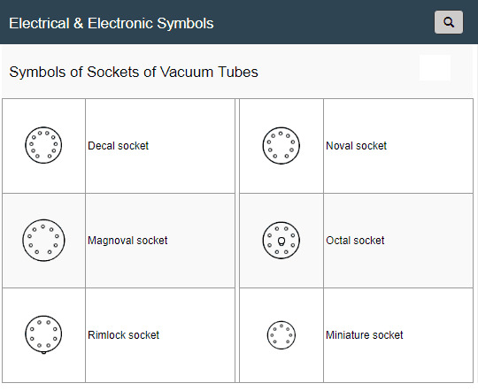
Symbols of Sockets of Vacuum Tubes
https://www.electrical-symbols.com/electric-electronic-symbols/vacuum-tubes-symbols.htm#symbols_sockets_vacuum_tubes
0 notes
Text
Evolution of Computer-Based Technologies and Morden Ethical Principles
In primitive societies, man began to use knotted ropes, stones, branches or inscriptions as tools to assist in calculation and counting. As mankind has always sought to improve the speed and accuracy of calculations: In 1620, European scholars invented the logarithmic calculating scale; in 1642, Blaise Pascal invented the mechanical computer; in 1854, George Boole, an English mathematician, introduced the idea of symbolic logic. I reckon early computer technology is not to be confused with digital technology, because the digital information processing capability of early computer technology is too weak, although it has the same essence as digital information but the capability is too far from it. In the 17th century, the German mathematician Leibniz invented binary, which created the conditions for the representation of data inside the computer. in the early 20th century, electronics technology developed rapidly, and in 1904, the British electrical engineer Fleming developed the vacuum diode. in 1906, the American scientist Forrester invented the vacuum triode In 1906, the American scientist Forrest invented the vacuum triode, which laid the foundation for the birth of computers. During World War II, in order to develop new artillery and other weapons, the U.S. Army Ordnance Department set up a ballistic research laboratory in Maryland. In order to solve the large number of ballistic calculation problems faced every day, the world's first computer, the ENIAC, was developed at the University of Pennsylvania in February 1946.The first generation of computers, which could only support some computing work, had no concept of operating system and supported only machine language, and required highly educated professional understanding to maintain and use. At that time, computers were manufactured using electronic tubes, which were very costly and very large in size. Subsequently, its development moved in the direction of small machines, developing operating systems, supporting assembly language, and the size kept getting smaller and the cost kept decreasing due to the development of hardware technology. Later on, high-level languages emerged, i.e., humans could develop computer functions through natural languages. And it was only after the advent of the fourth generation of computers — large-scale integrated circuit computers (after 1971) - that mankind truly entered the digital age. People‘s learn, live and work a lot with the Internet, home appliances will be organized into home networks managed by computers, and people can get the information they need at any place and any time with any device.
In the documentary of Ada Lovelace, I believe she is one of the most important person in computer development history and her discovery is the foundation of modern computer logic. Ada is regarded as the first computer programmer. She is the first person that realizing the machine had more abilities beyond pure calculation. After I read the reading material —“Black inventors and pioneers who have influenced the way we use the internet and technology today”, I have to say that the Dr Philip Emeagwali is also an important person in computer development history. He’s design in Connection Machine system is significant. Emeagwali built computer systems that could work and communicate internally like a honeycomb, and this innovation in computer systems guided the development of the Internet in a new direction. Almost all computer systems with search engines today have evolved from programs designed by Emeagwali. One of the influencing founding for me is that after I read so many material I found the female has rarely please in the history of computing or computer-based technologies. Form the reading material “Women in Computer Science: Getting Involved in STEM”, the report show only 18% of the of computer science bachelor’s degrees earned by females in the United States, however the Statistics from the National Girls Collaborative Project shows that female has half of the total U.S. college-educated workforce, but only 28% of the science and engineering workforce.
One of the key point made in readings material “Overview of Ethics in Tech Practice” which is interesting and also surprise me is the part of the concerns in Technology Ethics. In this part, the authors points is really the factors which often happen inner world. For example, the Rising Opacity, Algorithmic Bias and concentration of the wealth and power. This made me think about our society, I have to say the Morden Digital Age is new-born form, it involve a lot of changes in both wealth and power, so we need to cogitate the good and bad. One question I have is about the reading “A Framework for Ethical Decision Making”, after I read the part “Why Identifying Ethical Standards is Hard” I connecting with the today’s digital life, I found it is harder to identifying ethical standards in internet society. So could we use the existing social moral to identifying the digital ethical standards?
1 note
·
View note
Text
Electronic Tools
Electronics comprises the physics, engineering, technology and applications that deal with the emission, flow and control of electrons in vacuum and matter. It uses active devices to control electron flow by amplification and rectification, which distinguishes it from classical electrical engineering which uses passive effects such as resistance, capacitance and inductance to control current flow.

Electronics has had a major effect on the development of modern society. The identification of the electron in 1897, along with the subsequent invention of the vacuum tube which could amplify and rectify small electrical signals, inaugurated the field of electronics and the electron age. This distinction started around 1906 with the invention by Lee De Forest of the triode, which made electrical amplification of weak radio signals and audio signals possible with a non-mechanical device. Until 1950, this field was called "radio technology" because its principal application was the design and theory of radio transmitters, receivers, and vacuum tubes.
The term "solid-state electronics" emerged after the first working transistor was invented by William Shockley, Walter Houser Brattain and John Bardeen at Bell Labs in 1947. The MOSFET (MOS transistor) was later invented by Mohamed Atalla and Dawn Kahn at Bell Labs in 1959. The MOSFET was the first truly compact transistor that could be miniaturized and mass-produced for a wide range of uses, revolutionizing the electronics industry, and playing a central role in the microelectronics revolution and Digital Revolution. The MOSFET has since become the basic element in most modern electronic equipment, and is the most widely used electronic device in the world.
Electronics is widely used in information processing, telecommunication, and signal processing. The ability of electronic devices to act as switches makes digital information-processing possible. Interconnection technologies such as circuit boards, electronics packaging technology, and other varied forms of communication infrastructure complete circuit functionality and transform the mixed electronic components into a regular working system, called an electronic system; examples are computers or control systems. An electronic system may be a component of another engineered system or a standalone device. As of 2019 most electronic devices use semiconductor components to perform electron control. Commonly, electronic devices contain circuitry consisting of active semiconductors supplemented with passive elements; such a circuit is described as an electronic circuit. Electronics deals with electrical circuits that involve active electrical components such as vacuum tubes, transistors, diodes, integrated circuits, optoelectronics, and sensors, associated passive electrical components, and interconnection technologies. The nonlinear behavior of active components and their ability to control electron flows makes amplification of weak signals possible.
youtube
1 note
·
View note
Text
The vacuum pump prevents oil leakage
The vacuum pump prevents oil leakage
What sealing requirements do vacuum pumps have to prevent oil leakage
People who have used water ring vacuum pump know that the sealing of the equipment is a very important part of the process of use, must not be careless. If the sealing is done well, the vacuum drop can be avoided during use. If the seal work is perfunctory, then at some time the equipment will have a failure problem, resulting in its damage, not normal use, affecting our work efficiency.
Under its working pressure, the vacuum pump should drain all the gas produced in the process of vacuum equipment in time. Correct combination of vacuum pumps. Because the vacuum pump has selective pumping, therefore, sometimes choose a pump can not meet the requirements of pumping, need several kinds of pump combination, complement each other to meet the requirements of pumping. For example, titanium sublimation pump has a high pumping speed on hydrogen, but cannot pump helium, while triode sputtering ion pump, (or diode asymmetric cathode sputtering ion pump) has a certain pumping speed on argon, the combination of the two will make the vacuum device get a better vacuum.
The vacuum pump can not work under atmospheric pressure, need pre-vacuum, some vacuum pump outlet pressure is lower than atmospheric pressure, the need for the front stage pump, so the need to combine the use of the pump. Oil pollution requirements for vacuum equipment. If the equipment is strictly oil-free, should choose a variety of oil-free pumps, such as: water ring pump, molecular sieve adsorption pump, sputtering ion pump, cryogenic pump. If the requirements are not strict, you can choose to have an oil pump, and some anti-oil pollution measures, such as cold trap, baffle, oil trap, etc., can also meet the requirements of clean vacuum.
The vacuum pump should be installed in a firm and solid place on the ground. Under the vacuum pump base should maintain the level of the foundation, the four corners of the base is recommended to cushion damping rubber or bolt pouring installation, to ensure the vacuum pump smooth operation, small vibration.
The connection pipe between the vacuum pump and the system should be sealed reliably. For small vacuum pumps, metal pipe can be used to connect the gasket with oil-resistant rubber. For small vacuum pumps, vacuum hose can be used to connect.
1 note
·
View note
Photo


3D printed guitar pedals!
Blacklight diode compressor and Triode Sun tube overdrive. Get one on my Etsy store! https://www.etsy.com/shop/NuclearLighthouse
2 notes
·
View notes