#common PCB parts
Explore tagged Tumblr posts
Visit Tumblr Blog
Explore Tumblr blogs with no restrictions, modern design and the best experience.
Last Seen Tumblr Blogs


Fun Fact
The “We are the 99%” Tumblr blog became the slogan for the Occupy Wall Street movement.
Text
Explore the commonly used components in PCB assembly, including resistors, capacitors, diodes, and more. Learn how Viasion ensures high-quality assembly for reliable PCBs.
0 notes
Text
I took apart my cheap harbor freight multimeter cuz I was bored at work and noticed this
and I just gotta say that this is a really smart design


they made that little "finger" board part of the main board during fabrication and then snap it off and resolder it where it needs to go
this is really smart because then the actual fabricated PCB is a lot smaller so they can pack a whole bunch of them together and reduce the wasted substrate.
it's probably a common practice but I just think it's neat
that's awesome
5 notes
·
View notes
Text
Understanding Circuit Board Electronic Components: A Comprehensive Guide
In today's digital world, electronic devices have become an essential part of our daily lives. But what makes these devices tick? At the heart of every electronic device lies a circuit board—a masterpiece of tiny electronic components working together to perform complex tasks. In this article, we’ll dive deep into the fascinating world of circuit board electronic components, exploring each element’s role and how they contribute to the overall functionality of the device.
What is a Circuit Board?
A circuit board, often referred to as a PCB (Printed Circuit Board), is a flat board used to mechanically support and electrically connect various electronic components. These components work in unison to perform a specific task. Think of the circuit board as the skeleton and nervous system of an electronic device—it holds everything together and allows communication between parts.
Types of Circuit Boards
Single-sided PCB: Has one layer of conducting material.
Double-sided PCB: Contains two layers for components and connections.
Multi-layer PCB: Complex boards with multiple layers for advanced applications.
The Role of Electronic Components on a Circuit Board
Every electronic device you interact with is powered by a carefully designed circuit board filled with various components. These components might be tiny, but each one has a critical role in the operation of the device. Here's a breakdown of the most important electronic components you’ll find on a typical circuit board.
1. Resistors
Resistors are fundamental components that control the flow of electrical current. They resist the flow of electrons, hence the name "resistor." Their primary function is to reduce current flow, adjust signal levels, and divide voltages in a circuit. Without resistors, circuits would allow too much current to flow, potentially damaging other components.
Types of Resistors
Fixed resistors: Have a set resistance value.
Variable resistors: Allow adjustment of the resistance.
2. Capacitors
Capacitors store and release electrical energy in a circuit. They are often compared to small rechargeable batteries that quickly charge and discharge. Capacitors help smooth out fluctuations in voltage, filter noise, and store energy for future use.
Common Uses of Capacitors
Energy storage
Signal filtering
Voltage stabilization
3. Inductors
Inductors are components that store energy in a magnetic field when electrical current flows through them. They resist changes in current and are typically used in circuits to filter signals, manage power, and store energy.
Applications of Inductors
Power supplies
Radio frequency circuits
Noise suppression in circuits
4. Diodes
A diode is like a one-way valve for electricity, allowing current to flow in only one direction. They are vital in circuits to prevent reverse currents, which can damage components.
Types of Diodes
Light-emitting diodes (LEDs): Produce light when current flows through.
Zener diodes: Regulate voltage within a circuit.
5. Transistors
The transistor is a versatile component used to amplify or switch electronic signals. In essence, transistors are like tiny switches that turn signals on and off rapidly, making them essential in modern electronics.
Types of Transistors
NPN transistors: Allow current flow when a small voltage is applied to the base.
PNP transistors: Conduct when the base is negatively charged.
How Circuit Board Components Work Together
In a circuit, each component has a specific role, and together they form a cohesive system. For example:
Capacitors and resistors may work together to filter signals or smooth out voltage fluctuations.
Transistors and diodes ensure that signals are amplified or directed properly.
Integrated circuits handle the complex tasks, processing data, and controlling the overall system.
Choosing the Right Components for Your Circuit Board
When designing or repairing a circuit board, choosing the correct components is crucial. Some factors to consider include:
Voltage requirements
Power consumption
Signal type and frequency
Physical size and compatibility
Conclusion
Circuit boards are an integral part of any electronic device. The various components on the board each play a specific role in ensuring the device functions as intended. Understanding these components, from resistors to integrated circuits, is essential for anyone working with electronics, whether you're designing a new system or troubleshooting an existing one.
2 notes
·
View notes
Text
Ultimate Guide to PCB Testing Methods: Ensuring Quality and Reliability in Your Circuits
In the electronics sector, Printed Circuit Boards (PCBs) are the life-lines of virtually all gadgets that are in use in the modern society. From humble home appliances to gigantic industrial equipment, PCBs are the skeletal framework of hardware organization and connection of circuit elements. It is vital to guarantee the quality and dependability of these fundamental parts – thus enters PCB testing methods. It is our hope that this extensive hand will help identify the most suitable test strategies for PCB testing, why these techniques matter, and how to maximize your circuits’ functionality.
Introduction

Firstly, an increase in the capability of different electronic devices leads to higher necessary requirements to the PCBs used in their production. Performing tests on the PCBs is an essential step in the manufacturing process done to confirm that a given board performs as a unit to the expected levels. This guide aims at explaining various techniques of PCB testing with a view of having a better understanding on how to achieve quality and reliability on the circuits.
Why PCB Testing is Crucial

PCB Testing When it comes to the potential defects on PCBs, there are shorts, opens, and some component placements. They can cause device failure, decline in performance level, and sometimes also pose safety issues. Through high-quality testing regimes, it becomes easier to address problems before they reach the customer, and thus manufacturers will have reliable and efficient products. Key reasons for PCB testing include:
Detecting Manufacturing Defects: Solder bridges, missing and placed in wrong position components, all can be detected in the initial stages easily.
Ensuring Functionality: Ensuring that the PCB does what is wanted and needed when it is in use, and under several conditions.
Quality Assurance: Ensuring that the business meets industry standards, and what clients require of them.
Cost Efficiency: Decreasing the likelihood of rework and recall by identifying possible defects before they get to the customer.
Types of PCB Testing Methods
These are the types of PCB Testing Methods:
Visual Inspection

Technique one as also referred to as the VI or visual inspection is the simplest and basic type of testing done on PCBs. The technique entails inspecting the board with naked eyes for some of the common faults including solder bridges, missing parts, and misalignment issues.
Automated Optical Inspection (AOI)

AOI employs cameras and software algorithms to check PCBs for defects and performs the inspections singly. This method of inspection is far more efficient than the manual inspection and simultaneously versatile enough to identify numerous problems.
X-ray Inspection

Some functions which include examination of features of BPCs that could not be easily inspected include solder joints under components through x-ray inspection. It is especially effective in inspecting defects in BGA (Ball Grid Array) and other various packages as well.
In-Circuit Testing (ICT)
ICT entails applying different voltage across the PCB to checks on the electrical characteristics of the needy part and connections. The use of this method is highly recommended for the identification of functional problems and verification of the circuit’s goodness.
Functional Testing (FCT)
Functional testing evaluates the effectiveness of the PCB pointing to the fact that it can be tested when placed in use. This method enables the certification of that the PCB works as expected under actual environment.
Flying Probe Testing
In flying probe testing, the probes are moved around to test the electrical properties of the created PCB. Lower to medium volume production runs can be made easily by using this technique; hence it is advantageous in this regard.
Boundary Scan Testing
Boundary scan testing also called as JTAG testing extends test circuitry into all the components for testing the connections between them. Although, this method is very efficient for identifying connection problems and faults.
Burn-In Testing
Burn-in testing puts the PCB in a state of operational stress for a long time to capture early-life failures. This aspect makes the method reliable for the long term since it is likely to identify problems that may occur when the equipment is in use for a long time.
Detailed Analysis of Each Testing Method works
These are the detailed analysis of each testing method works:
Visual Inspection
Pros:
Simple and low-cost
Determined to be a system for the reporting of noticeable defects as soon as they are observed.
Cons:
Time-consuming for complex boards
Limited to visible defects
Automated Optical Inspection (AOI)
Pros:
Fast and accurate
Is capable of detecting various kinds of defects.
Non-destructive
Cons:
High initial setup cost
May need to have better settings optimized for specific boards.
X-ray Inspection
Pros:
Examines hidden features
Ideal for complex packages
Cons:
Expensive equipment
Requires skilled operators
In-Circuit Testing (ICT)
Pros:
Thorough electrical testing
High fault coverage
Cons:
Requires custom fixtures
Not for all the boards or servers that you wish to build.
Functional Testing (FCT)
Pros:
Ensures real-world performance
Detects system-level issues
Cons:
Time-consuming
The mathematical test object can involve complex arrangements of test configurations.
Flying Probe Testing
Pros:
Flexible and adaptable
Cost-effective for small batches
Cons:
Slower than ICT for big volumes
Applicable only when the board is specially designed
Boundary Scan Testing
Pros:
Interconnections have high fault coverage.
Said; No need to have physical access to the test points
Cons:
Requires boundary scan-enabled components
Complex setup
Burn-In Testing
Pros:
Identifies early-life failures
Ensures long-term reliability
Cons:
Time-consuming and costly
Perhaps stressful to the board
Choosing the Right Testing Method
The choice of the appropriate method of PCB testing can be influenced by several factors such as the level of complexity of the PCB and the numbers of boards to be tested as well as the actual costs of the testing process and other features. Consider the following when choosing a testing method:
Board Complexity: Great board densities or component placement can be a determinant as to whether one needs AOI or X-ray inspection.
Production Volume: Applications that are characterized by high volumes can be easily facilitated by ICT while the low to medium volume applications may require flying probe testing.
Budget: Both manual inspection and AOI are favorable for various production volumes, while X-ray and ICT are more expensive at the beginning.
Specific Requirements: There are two types of the test, namely Functional Test and Burn-In Test that should be made so as to attain the long term reliability in applications that are critical.
Best Practices for PCB Testing
Using the best techniques in testing PCBs increases the quality and reliability of the circuits that you are working on. Here are some key practices to follow:
Early Testing: It is recommended to carry out the tests when the product is still in its design and manufacturing phase so that problems can be noted earlier before they reach a very catastrophic level.
Automate Where Possible: Use method such as automation to reduce the time and improve on the quality of the testing.
Regular Calibration: It is necessary to check if all the testing equipment used for calibration are accurate.
Comprehensive Coverage: This way, you will be able to ensure that there are no defects that are not tested as the best testing approach combines all types of testing methods.
Document Everything: Ensure that you keep records of the tests performed, the results obtained, as well as any measures taken to correct the breaches.
Common Challenges and How to Overcome Them
These are the common challenges and how to overcome them:
False Positives/Negatives
Automated testing methods maybe good some times, they give you the results that are either positive or negative and this will lead to unnecessary rework or more alarming leaving critical defects unfound. In order to avoid this, make sure that testing algorithms and testing equipment are updated and fine-tuned from time to time.
Component Access
Some of the testing techniques involve handling parts of the circuit and with high density board this can be very difficult. Some of the ways in which testbench implementation can be avoided are as follows Boundary scan testing and X-ray inspection.
High Costs
Some form of testing such as X-ray and ICT testing is often very costly. The effectiveness must come with reasonable prices; try to combine some of the mentioned approaches to cover all the aspects without spending too much money.
Future Trends in PCB Testing
About the future, it can be stated that its trends will be in fact linked to the tendencies in technologies and expectations towards ever higher quality and quantity of tested PCBs. Key trends to watch include:
AI and Machine Learning: Using of intelligence algorithms and machine learning in testing algorithms to enhance the efficiency and the minimization of false negative or false positives.
IoT and Smart Manufacturing: Higher testing flexibility and opportunities for the continuous test process supervision.
Advanced Imaging Techniques: The need for better techniques that would enhance the detection of defects within a printed circuit.
Environmental Stress Testing: More focus in the testing of PCBs under different environmental pressures in order to improve on its longevity.
Conclusion
Quality and reliability of packaged circuits have to be maintained to contribute positively in any electronic equipment. This paper seeks to explain the common testing techniques for PCB so that PCB manufacturers are able to test and see if they are free from defects and if they are functional. This ultimate guide will give you a full insight on the available options in PCB testing that will enable you make the best decision that will give you perfect circuits.
The aim is to help you understand how to attain the best quality of PCBs, what methods are worth following, and what trends drive future improvements, thus contributing to the quality of the final electronic products and, consequently, consumer satisfaction.
#PCBTesting#Electronics#CircuitBoard#QualityControl#Engineering#Technology#Manufacturing#IndustrialDesign#Tech#Innovation
2 notes
·
View notes
Text
Printed Circuit Board Basics
Most of us are using Printed Circuit Board in our daily life. Printed Circuit Boards are used in almost all the Electronic products, from consumer gadgets such as PCs, tablets, smartphones, and gaming consoles to industrial and even high tech products in strategic and medical electronics domains.
Here, we have some statistics for you that shows how many electronic devices connect worldwide from 2015 to 2025. This statistic shows an increase in the use of a number of PCB in people daily life. Hence, CircuitWala took this opportunity to provide a basic knowledge about PCB via this article.
There are so many books available online which teach about Printed Circuit Board design and hardware part. There are few links available online which shows only a few basic fundamentals of PCB and few are there for Basics of Printed Circuit Board (PCB) Design. Few which gives good know knowledge on Printed Circuit Board terminology. But in the end for the hobbyist, there is no such material available which make their work easy.
Now days there few online designing websites available which allow hobbyist and students to create their design and Printed Circuit Board fabrication part. These websites provide limited features and charge high for the full edition. We, @CircuitWala are in try to provide one platform which provides plenty of Printed Circuit Board knowledge digitally to make your work simple and easy.
Alternatives of PCB include wire wrap and point-to-point construction. Creating a layout of PCB is a little bit time-consuming method as compared to its alternative solution but manufacturing of PCB is cheaper and faster then other wiring methods as electronic components are mounted and wired with one single part.
Let’s start with some basics of Printed Circuit Board with this article. Here in this article we will discuss about history of PCB to understand the emerge of PCB, Types of PCB to make your complex PCB a very simple using different types, Usage of PCB to provide you an idea to create more Printed Circuit Board projects, Advantages and Disadvantages, Possible Future to know about new technological change in Printed Circuit Board manufacturing and also about how to destroy and manage your PCB’s e-waste? We know you are eager to know all the stuff in details but before that let’s make a simple definition of Printed Circuit Board.
What is Printed Circuit Board?Printed Circuit Board is an electronic device made of conductive material(FR-4) like copper which connects components mounted on it to to get desired output by providing an input on another end.
When the board has not mounted with any of the components is called as Printed Circuit Board or Printed Wired Board. Mounting of an electronic component on Printed Circuit Board is called as PCB assembly.
History of Printed Circuit BoardThe invention of Printed Circuit Board was by Austrian engineer Paul Eisler as part of a radio set while working in England around 1936.
In early days before Printed Circuit Board became common in use, Point-to-Point construction was used. This meant some bulky and unreliable design that required plenty of sockets and regular replacement of it. Most of this issue directly address when PCB went into regular production.
Originally, every electronic component had wire leads, and the PCB had holes drilled for each wire of each component. The components’ leads were then passed through the holes and soldered to the PCB trace. This method of assembly is called Through-Hole construction. There is one other method to mount component is called as Surface Mount.
Type of Printed Circuit BoardPCBs are produced from the different types of material and on the basis of that material PCBs are divided mainly into two parts: Rigid PCB and Flexible PCB. Nowadays, a combination of Rigid and flexible PCB is also possible and that is called as Flexi-Rigid PCBs.
Most of the PCBs are built in layers. The inner layer is the base material called as a substrate. Rigid PCBs are mainly made of material like epoxy materials and Flexible PCBs are made of plastic material that can withstand high temperatures.
Rigid PCBs are generally, hard materials that hold the component in a better way. The motherboard in the tower of a computer is the best example of Rigid PCBs. Flexible PCBs fundamental material allows PCB to fit into forms that Rigid PCBs can not. Flexible PCBs can turn round without harmful the circuit on PCB.
All Rigid and Flexible PCBs can come in three formats by layers: Single Layer, Double Layer, and Multi-Layer.
1. Single Layer PCBSingle Layer PCBs have been around since the late 1950s and still dominate the world market in sheer piece volume. Single Sided PCBs contain only one layer of conductive material and are best suited for low-density designs. Single-sided PCBs are easy to design and quick to manufacture. They serve as the most lucrative platform in the industry.
2. Double Layer PCBDouble Layered printed circuit board technology is conceivably the most popular type of PCB in the industry. Double Sided PCB (also known as Double-Sided Plated Thru or DSPT) circuits are the gateway to advanced technology applications. They allow for a closer (and perhaps more) routing traces by alternating between top and bottom layers using vias.
3. Multi Layer PCB
Multilayer PCB is a circuit board that has more than two layers. Unlike a Double-Sided PCB which only has two conductive layers of material, all multilayer PCBs must have at least three layers of conductive material which are buried in the center of the material.
Usage of Printed Circuit BoardBy reading this article till this point, we hope that you are now able to get about printed circuit boards. Now, we will make you understand about different applications of printed Circuit Board.
In this digital world, Printed Circuit Board is in almost all our daily life electronic devices and in our industrial electronics as well. Below are the industries where PCBs are used:
Possible FutureNowadays, most of the circuits are replaced to produce Printed Circuit Board from the old methods. Revolution in technology made many of the processes automated and hence it is easy to manufacture PCB. But still, these processes are a bit expensive to hire, involve toxic waste and use high temperatures and acids. With technological advances we have seen in the past years, it is not hard to imagine PCB will soon be revolutionized. Not only that but research institutes predict a more ‘green’ future for PCBs; PCBs being made of paper.
Electronic Waste (e-waste)Electronic Waste or e-waste is described as discarded electrical or electronic devices. Informal processing of e-waste in developing countries can lead to adverse human health effects and environmental pollution.
Electronic scrap components contain a hazardous substance such as lead, cadmium, beryllium, or brominated flame retardants. Recycling and disposal of e-waste may involve significant risk to health of workers and communities in developed countries and great care must be taken to avoid unsafe exposure in recycling operations
Nowadays, developing countries are encouraging electronic users to take care while recycling the e-waste or submit them to the organization who are involved in such activities.
SummaryIn this blog, we have learned the basics of Printed Circuit Board. CircuitWala is planning to write as many blogs to provide more and more knowledge of Printed Circuit Board. Either it is basics or manufacturing or usages or advantages and disadvantages of PCBs. We will also try to make our users/customers up to date for the new technology innovations, including past histories and revolution of the PCB industries.
In the next blog, we will look at more briefly about the different types of Printed Circuit Board. We also understand the process to make it and different usage and application for the same.
#electronic circuit design company#pcb circuit manufacturer in ahmedabad#pcb design & manufacturing services#printed circuit board companies#printed circuit board order online#PCB manufacturer#Printed Circuited Board#double layer PCB#PCB Quality Control
2 notes
·
View notes
Text
What is PCB Assembly ?
PCB Assembly manufacturer - Hitech Circuits Co., Limited
It’s the step in the manufacturing process in which you populate a blank board with the electronic components needed to make it into a functional printed circuit board. It’s these components that make a board into the circuit that enables an electronic product to function. PCB assembly typically takes place via one of two processes:
1. Surface-mount technology
SMT: SMT stands for “Surface Mount Technology“. The SMT components are very small sizes and comes in various packages like 0201, 0402, 0603, 1608 packages for resistors and capacitors. Similarly for Integrated circuits ICs we have SOIC, TSSOP, QFP and BGA.
The SMT components assembly is very difficult for human hands and can be time taking process so it is mostly done by automated pick and place machine.
2. Through-hole manufacturing
THT: THT stands for “Through hole Technology”. The components with leads and wires, like resistors, capacitors, inductors, PDIP ICs, transformers, transistors, IGBTs, MOSFETS are example.
The component has to be inserted on one side of PCB and pulled by leg on other side and cut the leg and solder it. The THT components assembly is usually done by hand soldering and is relatively easy.
Printed Circuit Board Assembly Techniques
There are only two common PCBA techniques available for use by a PCB designer. The methods are:
1. Automated PCB Assembly Techniques
Generally, this technique employs the use of state of the art machines, which are fully automatic. For example, the surface mount components are worth positioning with the aid of an automated pick and place machine.
Again, reflow soldering is commonly for surface mount components usually done in a reflow oven. An automated solder stencil is also used to apply the solder paste on the PCB.
Finally, high tech inspection machines are used to confirm and check the quality of the PCBA. Some of which include: Automated optical inspection machine (AOI), X-ray inspection machines, etc.
Above all, due to the precise monitoring, control of soldering, no human input and versatile machines.
This technique ensures utmost efficiency, output consistencies, and limits defects.
2. Manual PCB Assembly Techniques
This method is favorite for use with through-hole parts, which needs manual placement on the board. Besides, with these through-hole parts, it’s advisable you use wave soldering. Note that in the through- hole assembly process, you need to place the components and electronics on the PCB.
After that, you use wave soldering to solder the leads. Typically, you will need an individual to insert a component into a marked PTH. Once done, transfer the PCB to the next station where the next person will be on standby tasked with fixing another part.
What are the Benefits of SMT PCB Assembly?
SMT assembly provides many benefits and some of them are as follows:
It can be used to incorporate small components.
In SMT, the components can be placed on both sides of the board.
It assures high component densities.
Fewer holes need to be drilled for surface mounting than through-hole.
It require low initial costs and time for setting up the mass production.
SMT is the simpler and faster-automated assembly when compared to through-hole.
Errors regarding the component placement can be easily rectified.
Surface mount PCBs feature strong joints, which can easily withstand vibrations.
What are the techniques used in Surface Mount Technology?
There are several techniques for the reflow process. After applying the solder paste or a flux mixture on the board and after placing the components, the boards are conveyed to a reflow soldering oven. The techniques used for reflowing soldering include infrared lamps, hot gas convection, fluorocarbon liquids with a high boiling point, and so on.
What are the different testing methods used in SMT PCB Assembly?
Hitech Circuits as the PCB assembly manufacturer, we perform the following testing and inspection to ensure the quality of surface mount PCBs.
Automated Optical Inspection (AOI): This is performed before and after the soldering to identify the component placement, presence, and solder quality.
X-ray Testing: In this type of testing, the operator relies on the X-ray images of the PCB to check the solder joints and lead-less components such as Quad Flat Packs and ball grid arrays, which are generally not visible to naked eyes.
In-Circuit Testing (ICT): This method is used to detect manufacturing defects by testing the electrical properties in the SMT Assembly.
What type of files or documents should I send for SMT PCB Assembly?
Gerber Files: The file contains all details of physical board layers including solder masks, copper layers, drill data, legends, and so on.
Bill of Materials (BOM): This contains information on the list of items needed for the PCB manufacturing and the instructions of manufacturing.
Pick and Place File: This file contains information on all components to be used in the PCB design and their rotation and X-Y coordinates.
The whole process of PCB Assembly
1. Bare board loader machine
The first step in the PCB assembly is to arrange the bare boards on the rack, and the machine will automatically send the boards one by one into the SMT assembly line.
2. Printing solder paste
When PCB on the SMT production line, firstly, we have to print solder paste on it, and the solder paste will be printed on the pads of the PCB. These solder pastes will be melt and solder the electronic parts to the circuit board when it passes through the high-temperature reflow oven.
In addition, when testing new products, some people will use film board/adhesive cardboard instead of solder paste, which can increase the efficiency for adjusting the SMT machines.
3. Solder paste inspection machine(SPI)
Since the quality of solder paste printing is related to the quality of welding of subsequent parts, some SMT factories will use optical machine to check the quality of solder paste after printed the solder paste in order to ensure stable quality. If there any poorly printed solder paste board, we will wash off the solder paste on it and reprint, or remove the excess solder paste if there is redundant solder paste on it.
4. High speed SMT machine
Usually, we will put some small electronic parts (such as small resistors, capacitors, and inductors) to be printed on the circuit board first, and these parts will be slightly stuck by the solder paste just printed on the circuit board, so even if the speed of printing is very fast and the parts on the board will not fall away. But large parts are not suitable for use in such high speed SMT machines, which will slow down the speed of small parts assembly. And the parts will be shifted from the original position due to the rapid movement of the board.
5. Universal SMT machine
Universal SMT machine is also known as "slow machine", it will be assembled some large electronic components, such as BGA IC, connectors, etc., these parts need more accurate positions, so the alignment is very important. Use a camera to take a picture to confirm the position of the parts, so the speed is much slower than High speed SMT machine we taked before. Due to the size of the components here, not all of them are packed in tape and reel, and some may be packed in trays or tubes. But if you want the SMT machine to recognize the trays or tube-shaped packaging materials, you must configure an additional machine.
Generally, traditional SMT machines are using the principle of suction to move electronic parts, and in order to place the parts successfully, and there must be the flat surface on these electronic components for the suction nozzle of the SMT machine to absorb. However, for some electronic parts don’t have a flat surface for these machines, and it is necessary to order special nozzles for these special-shaped parts, or add a flat tape on the parts, or wear a flat cap for thees electronic parts.
6. Manual parts or visual inspection
After assembled all parts by the high speed SMT machine or Universal SMT machine and before going through the high-temperature reflow oven, and we will set up a visual inspection station here and to pick out the deviation parts or missing components boards etc., because we have to use a soldering iron to repair if there are still defectives boards after passing the high-temperature oven, which will affect the quality of the product and will also increase the cost. in addition, for some larger electronic parts or traditional DIP parts or some special reasons cannot be processed by the SMT machine before, they will be manually placed on pcb here.
7. Reflow oven
The purpose of reflow oven is to melt the solder paste and form a non-metallic compound on the component feet and the circuit board, that means to solder electronic components on the circuit board. The temperature rise and fall curves often affect the soldering quality of the entire circuit board. According to the characteristics of the solder materials, usually the reflow oven will set the preheating zone, soaking zone, reflow zone, and cooling zone to achieve the best soldering effect.
For example, the melting point for SAC305 solder paste with lead-free is about 217°C, which means that the temperature of the reflow oven must be higher than the melting points to remelt the solder paste. What's more, the maximum temperature in the reflow furnace should not exceed 250°C, otherwise many parts will be deformed or melted because they cannot withstand such a high temperature.
Basically, after the pcb passed through the reflow oven, the assembly for the entire circuit board is almost complete. If there are hand-soldered parts, we need to transfer to DIP process, and then we have to check the quality after reflow oven by QC department.
8. Automatic optical inspection(AOI)
The main purpose of setting up AOI is because some high density boards can’t be process the following ICT test, so we used AOI inspection to replace it. But even using AOI inspections, there still have the blind spots for such checking, for example, the solder pads under the components cannot be checked by AOI. At present, it can only check whether the parts have side standing issue, missing parts, displacement, polarity direction, solder bridges, lack of soldering etc., but cannot checking the BGA solderability, resistance value, capacitance value, inductance value and other components quality, so far AOI inspection can’t completely replace ICT test.
Therefore, there is still some risk if only AOI inspection is used to replace ICT testing, but ICT test is also not 100% make sure the good quality, we suggest these two ways can be combined with together to make sure the good quality.
9. PCB unloader machine
After the board is fully assembled, it will be retracted to the unloder machine, which has been designed to allow the SMT machine to automatically pick and place the board without damaging the quality for PCB.
10. Visual inspection for finished products
Normally there will be a visual inspection area in our SMT production line whether there is an AOI station or not, and it will help to check if there are any defectives after completed assembled the pcbs. If there is an AOI station, it can reduce the visual inspection worker on our SMT line, and to reduce the potential cost, and because it is still necessary to check some places that cannot be judged by AOI, many SMT factories will provide the mainly visual inspection templates at this station, which is convenient for visual inspection worker to inspect some key parts and polarity for components.
11. DIP process
DIP process is a very important process in the whole PCBA processing, and the processing quality will directly affect the functional for PCBA boards, so it is necessary to pay more attention to the DIP process. There are many preliminary preparations for DIP process. The basic process is to re-process the electronic components first, like to cut the extra pins for some DIP components, our staff received the components according to the BOM list, and will check whether the material part numbers and specifications are correct or not, and performs pre-production pre-processing according to the PCBA samples. The steps are: Use various related equipment (automatic capacitor pins cutting machine, jumper bending machine, diode and triode automatic forming machine, automatic belt forming machine and other machines) for processing.

12. ICT test
Printed Circuit board open/short circuit test (ICT, In-Circuit Test), The purpose of ICT test is mainly to test whether the components and circuits on the printed circuit board are open or short issues. It can also measure the basic characteristics of most components, such as resistance, capacitance, and inductance values to judge whether the functions of these parts are damaged, wrong parts or missing parts etc. after passing through the high-temperature reflow oven.
ICT test machines are divided into advanced and basic machines. The basic ICT test machines are generally called MDA (Manufacturing Defect Analyzer). It’s just to measure the basic characteristics of electronic components and judge open and short circuits issue we talked above.
In addition to all the functions of the basic ICT test machines, for advanced ICT test machine can also test the whole PCBA by using power, start to testing the PCBA boards by setting the program in the test machine. The advantage is that it can simulate the function of the printed circuit board under the actual power-on condition, this test can partly replace the following functional test machine (Function Test). But the cost for the test fixture of this advanced ICT test can probably buy a car, it’s too expensive and we suggest it can be used in mass production products.
13. PCBA function test
Functional testing is to make up for the ICT test, because ICT only tests the open and short circuits on the the PCBA board, and other functions such as BGA and other fuctions are not tested, so it is necessary to use a functional testing machine to test all functions on the whole PCBA board.
14. Cutting board (assembly board de-panel)
Normally, printed circuit boards will be produced in panel, and it will be assembled to increase the efficiency of SMT production. It means several single boards in one panel, such as two-in-one, four-in-one etc. After finished all the pcb assembly process, it needs to be cut into single boards, and for some printed circuit boards with only single boards also need to cut off some redundant board edges.
There are several ways to cut the printed circuit board. You can design the V-cut using the blade cutting machine (Scoring) or directly manually break off the board (not recommended). For more high density circuit boards, it will be used the professional splitting machine or the router to split the board without any damage the electronic components and printed circuit boards, but the cost and working hours will be a little longer.
Why Choose Hitech Circuits PCB Assembly Manufacturer for Your PCB Assembly Projects?
There are several PCB manufacturers specializing in PCB assemblyservices. However, Hitech Circuits PCB Assembly stands out owing to the following:
Assistance in Material Procurement:
Technically, in PCB assembly services, the quality of parts is the responsibility of the OEM; however, we ease your job by assisting you to make the right selection. We can help you procure all your parts of the same type own a single part number, thanks to our supply chain and vendor network as well as experience. This saves time and cost that goes in ordering single parts as you plan.
Testing procedures:
We are very focused on quality and thus implement stringent testing procedures at each stage of the assembly and after completion.
Fast Turnaround Times:
Our well-equipped facility and the right tools enable us to complete your requirements well before time, and without compromising on the quality or functioning of the PCBs. For simple designs we revert in 24 to 48 hours.
Cost Effectiveness:
While PCB assembly is a cost-effective alternative, we go a step further and assure that the parts you list are of a good quality and suitable for your requirement. Also, you can control the part flow and replenish them as needed. This eliminates the need to buy extra stock and store it.
Quick Quote:
We offer a quick quote based on your BOM. All you need is a detailed BOM, Gerber files, your application requirement sheet, and quantity.
We’re not one to stand still, which is why we use the latest equipment and the finest minds to create your PCB projects. We’re constantly keeping our finger on the pulse of the latest trends. And as a result, we know how to deliver the highest standards of PCB assembly to meet all your requirements.
Our dedicated, friendly customer service team also means that we support you every step of the way. Offering our expert guidance to ensure a complete PCB project that you’re happy with.
Contact us today
No matter what your printed circuit board assemblyneeds are, we always aim to deliver efficient, dependable solutions. For more information about our services, do not hesitate to get in touch with us today for a no-obligation quote
2 notes
·
View notes
Text
On Autonomy in the IT Industry
What's kinda frustrating for a disabled hardware geek like me is that a lot of my peers don't really see how common maintenance tasks are day-long planning and execution rigamaroles for me. Those tiny M.2 screws? They're a bitch to wrangle if your hind brain is so convinced you'll drop it in the frame that your limbs are overtaken by tremors so strong that the entire case shakes.
At the Old Place, my former boss used to give me an amused look. "Relax, Grem! It's just a single screw; you can't mess this up!" she'd say.
The fact is, I could - and I knew it. I've scratched material off of PCBs, shorted boards, lost screws, broke posts and scrapped hardware all because my motor controls never got the message that I know how to handle a PC case in multiple formats. The old boss never understood why I needed to force myself into borderline monastic levels of focus to switch M.2 drives out of a system, or why I demanded near-absolute quiet when my colleagues could shoot the shit while handling a laptop's stumpy little external screws.
Walt and Sarah, however, understand this all too well. I updated my Steam Deck's SSD last night, and both of them treated this like I were a heart surgeon performing a triple bypass. Others might've laughed, but I was actually given the space I needed, for a change. The same went for the Palpatine server - the more crucial operations always came with a ramping-down of Walt's phone calls.
What they also understand is that pushing past my disability and succeeding feels insanely good. I walked out of mine and Walt's room with a big-ass grin and a functional 1 TB Steam Deck in hand with no stripped screws or broken screw posts, and I was proud of myself. Sarah gave me a wolf whistle and Walt added a golf clap in equal parts supportive and teasing measures.
I doubt many able-bodied techs get that feeling; this "I did something! Me, on my own, without ever asking for help! Yes!" type of euphoria that I've only ever seen out of cripples like me when we both manage to pull ourselves by our bootstraps and materially succeed in what we'd envisioned. Able-bodied people tend to downplay most of what they do, but even switching RAM sticks without missing the slots at least four or five times still feels like a big thing for me - and I've been building PCs for about twenty years, now. Plus, the older I get, the more demanding some operations become. It makes successes all the more precious - and increasingly less banal.
#disability#IT post#self-reliance#autonomy#adulting#pride#an actual sense of accomplishment#yay i screwed in this tiny screw and didn't strip everything i'm the best#something able-bodied techs always look a little flummoxed by#it's not that I feel like I'm five it's that it's hard
2 notes
·
View notes
Text
Just got something in from the PCB manufacturer! It's something between an art project, a gag, and an attempted scam.
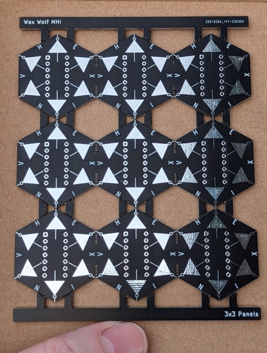
I tried making these as a panelized set of circuit boards; the units are the individual hexagons, which — if I got these right — should snap apart along the lines marked by the tiny drill holes. Each one has just one component to be mounted on it.
What am I doing with these? Lemme tell you a story.
It's pretty common knowledge that the CIA got up to some very weird stuff in the 1950s-70s. One aspect was a project now known under the umbrella code name MKULTRA, which involved illegal human experimentation in "brainwashing" and inducing altered states. MKULTRA is best known for administering LSD to unwitting victims, though as a giant research project, the people running it considered many paths to the same goals. A subprogram or successor program (accounts vary) known as MKOFTEN sought out any means possible to make human minds malleable — and, importantly, to protect its own agents from the same — including chemical and biological methods, but also researching psychics, mediums, and practitioners of black magic. Even decades after the MKULTRA programs were officially shut down in 1973, the CIA still sponsored research into psychic remote viewing as Project Stargate.
I cannot prove that any of the above has anything to do with the heart of this device, but while I can't demonstrate that the chips for these boards were made expressly for this purpose, it is instructive that part of the mandate was defending against all these dark magics — and the parts were provably made to Department of Defense specifications. These amulets, designed to turn all sorts of offensive magics, psychic vampirisms, and instances of the Evil Eye upon you to the positive — to turn all Bad Juju to pure Good Vibes — are made to house, once assembled, a genuine SN5404 TTL chip: a military-grade Hex Inverter.
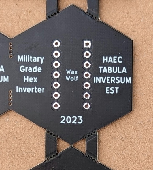
Or at least that's the core of the sales pitch. I think the final item listing needs to mention that these use psychotronics, that branch of electronics that develops devices to boost or even create the user's psychic powers. See, researchers in this field long ago made the amazing discovery that various materials used in their circuits could be swapped for different materials without measurably affecting their effectiveness. In fact, proponents will tell you, you can actually take the whole circuit out and replace it with a simple drawing of the circuit, and it'll work just as well!
(The full significance of that last statement is left as an exercise for the reader.)
(When I first came up with this, I was going to offer a large cash refund to anyone who could demonstrate that a paranormal effect with any ill intent got past the amulet — but the James Randi Educational Foundation is no longer offering their million dollar prize, so the plan to use their proof to claim that cash and pay out afterwards won't work.)
2 notes
·
View notes
Text
FEATURE: Kaisa sa Musika: The Return of UP Fair

UP Fair 2023 Kaisa ka sa Musika pubmat. Retrieved from https://www.facebook.com/UPFair/
After being stagnant for many years, the most anticipated week among UP students is back. The UP Fair consists of five days. Each one has its own unique flavor as it's usually organized by different groups that invite a wide variety of artists. Here, numerous booths and rides can be found, but hidden under the guise of an entertainment event for dancing the night away with friends are advocacies that the UP student body at large fights for. Despite the promise of exciting activities and attractions, the real goal of these five days is to provide a platform for numerous people to have their voice, and what they fight for, heard.
Join us as we take a look at what each day brought to the table and what their noble endeavors were.
REV

Lively crowd gathered during REV 2023. Retrieved from: https://www.facebook.com/REVpresents/photos/pcb.3472620732952801/3472620672952807
The first day of the event was UP Fair REV; its advocacy centered on the issue of injustice and lack of accountability from our government. They called out the state for its crimes against human rights—specifically during the regime of Duterte and Marcos Sr., as the victims were never given any justice while the real perpetrators of said crimes still run free with a clean slate under their names.
UPIS alumnus Kobe Rivera from batch 2019 Ignite, is part of an organization that was in partnership with the REV committee. This is a common occurrence as numerous partnerships are made among organizations that have a passion for a common cause at a big event such as this. According to him, the advocacies of each day are important, and based on his experience during REV, he noted that they were successful in their goal of providing necessary information to the attendees.
Though he also noted a recurring happening that can be improved—he noticed that the organizers sometimes fail to get the people’s attention. "When the advocacy starts, a lot of people use it as a time to buy food and drinks rather than to listen," he said, the numbers of those who join and actively listen to the advocacy are relatively low as compared to the hype that people give to the performing bands. But even so, he cannot deny that the appeal of the fair did not lessen because of that.
He is actually an avid enjoyer of the fair as he has been going for years. He noticed that the sets were shorter and were bitin for him since it is what he came for, but he still enjoyed it regardless, as he managed to catch up with his high school friends as they went through all the booths and rides.
KALYE TUNES

A picture of the advocacy segment during Kalye Tunes showing their stand on jeepney phaseout. Retrieved from: https://twitter.com/kalyetunes/status/1631613876134625282/photo/1
The next day was the day to light up the spirit of local hip hop—Kalye Tunes. On brand with their name, they dedicated their advocacies to both our jeepney drivers and the people who live in slums. Kalye Tunes advocated for something that is a hot topic—one that has been brought to the fore by the recent strike of transport groups: jeepney phaseout. Their other advocacy is fighting against big corporations and how their actions cause many families to be forced out of their homes and live in unsuitable areas. They featured the case of Sitio San Roque, whose people have been trying to reclaim their land after having been evicted from it.
The combination of music that matched the taste of the mass and advocacy on an issue that almost everyone is affected by, made this day one of the most sought-after. Kiel Beldia, a student from 12-Kamalayan, surely made it his goal to be a part of such a big event, as he was part of the volunteer corps of Kalye Tunes. Though it was not his first time attending UP Fair, it was still a new experience as volunteering for it revealed hidden sides of organizing the event, which just made him more passionate about its cause. But being a volunteer doesn’t mean all work for him; he still got to enjoy the event and even had time to roam around and have a go at the rides such as the Viking, and of course, he also got the chance to jam with an artist that he was excited to hear from: Al James.
DIMENSIONS

Mayonnaise during Dimensions. Retrieved from: https://twitter.com/mayonnaisemusic/status/1626241089488429058/photo/1
The third day of the fair is probably the one that made the most uproar. Dimensions was the talk of the town as they were early to release parts of their lineup, thus, hyping up the students to buy tickets early. Such a simple strategic move, yet, was very effective. The selling for this day was the most brutal out of all the days, but one that was still worth all the efforts for its attendees. Another smart move of its organizers was their choice of advocacy—somewhat a natural continuation of what came the day before: the country’s transportation crisis. Who wouldn't want to go to an event whose advocacy affects the everyday life of every single Filipino?
Another reason for this day to be the crowd's favorite is that the whole setlist was the best—Annika Porto of grade 11-HT Sy, Sr. clearly thinks so. Among the bands, she was really looking forward to Mayonnaise, Lola Amour, and The Itchyworms. She even mentioned that she has always been on the lookout to experience attending a performance of Mayonnaise. She was put out when she couldn't attend UP Fair 2020 to see them, and so she was ecstatic to tell us how she enjoyed and sang her heart out to their song Jopay.
The name Dimensions might not ring a bell among usual fair-goers, as they were more familiar with the name Roots for the usual Thursday fair, but to those that do not know, both actually have the same organizer which is the UP Economics Society. This rebranding might have been for the better. Annika loved the energy that Dimensions had and she even noted that the planning for crowd space was much more organized as it was divided into two sections, unlike in the past where the audience was compacted all together in the middle.
POLARIS

MRLD celebrated her birthday with the Polaris crowd. Retrieved from https://twitter.com/UP_Fair/status/1626648650620493825?s=20
The fourth day of the fair, Polaris, held a variety of advocacies that are more catered toward the student body of the university. As students of the University of the Philippines, we continuously strive and fight for academic freedom, opposing campus militarization and any form of oppression. Having programs for equality and inclusivity, along with gender-responsiveness and cultural sensitivity—these are what Polaris fights for as well.
But, it is worth taking note that the organizers for this day, the UP Upsilon Sigma Phi, have sparked some disputes and have been known for making statements that contradict the very advocacy of the event, proving all the more the need to fight for equality and inclusivity. Though filled with controversies, that is not a reason to discount the efforts of numerous people and its attendees to fight for the day's advocacy.
Pauline Vargas, a current grade 11 student in the Business and Entrepreneurship track, is one of many that got to hear these advocacies live. According to her, some of the reasons that made her choose to attend the fair day was due to the fact that she resonated with what they were fighting for, and also because of the convenience of the schedule. Not new to attending the fair, she stated that the recent experience differed from others by how they effectively communicated their advocacies to the crowd; the fairs of the previous years were not that successful in voicing out what they were fighting for.
As the students and goers of the fair celebrated and enjoyed the rest of the night, bands and performers like December Avenue, I Belong to the Zoo, Orange & Lemons, MRLD, and more serenaded the crowd that willingly held up their phone flashlights, creating an illusion of a starry night from the artists’ point of view.
The event’s advocacies did not only last for the night, as the organizers extended help towards the students that went beyond the fair day's closing hours. Pauline’s highlight for the night was when Polaris announced that they covered the dormitory fees of all UPD students for one semester.
COSMOS

Ben&Ben performing at Cosmos. Retrieved from: https://twitter.com/CosmosOPMFest/status/1630575556432633856/photo/3
Cosmos, the day where the UP Sunken Garden grounds became a safe space for all—regardless of gender, sexuality, and expression—was held on the fifth and last day of the fair, ending it with a bang. Handled by the UP Junior Marketing Association, the fair day’s advocacies revolve around the promotion of trans rights, the SOGIE equality bill, reproductive health for all, and inclined with National Women’s Month this March, Cosmos also advocates for feminism.
Gian Manalo, a UPIS Batch ‘22 Doble Dos alumnus, expressed how Cosmos became his go-to UP Fair day, and attending every year turned into his own personal tradition. Compared to his previous Cosmos experiences, this year's crowd was especially bigger because of the demand, due to the fact that it has been a while since the fair was last held. According to him, getting tickets felt almost like a lottery by how difficult it was to purchase them. He also observed that there were more non-UP students compared to UP students, resulting in a much different hype, but nonetheless, it was good that more people were exposed to the advocacies that day had.
What made Gian’s night incredibly special was the performance that BINI, an eight-member P-pop girl group, offered to the fairgoers. More widely-known bands were part of the night’s lineup, such as Moonstar88, Autotelic, The Itchyworms, Ben&Ben, and more. And, although his favorite ride wasn’t included in the most recent UP Fair, Gian said he still very much enjoyed the Viking.
With the UP Fair officially back once again, it certainly has brought a sense of hope and something most students can look forward to, whether they may be from inside or outside the campus. For anyone that is interested and is now planning on attending the next UP Fairs, our beloved schoolmates left a few words of advice to make your next fairs worthwhile.
“Go with someone you hold close and dear to your heart or your very sabog friends! Witnessing music live is way more enjoyable and wholesome with company you like because it brings out all the feels, emotions, hype, you name it!” —Gian Manalo, Doble Dos.
"Bring some mats if your feet/legs are weak and if you are going to stand for the whole time." —Pauline Vargas, Grade 11.
"Prepare for when it rains because we were fortunate that rain was not present for the whole week. But if rain was to come you should have plastic bags or ziplocks ready for your belongings." —Kiel Beldia, Grade 12.
"Always be alert and be mindful of your things. As much as possible, don't bring a backpack and use sling bags instead to prevent yourself from losing things. Explore the booths and rides inside the fairgrounds and the most important thing you need to remember is to enjoy the performances! Don't be shy to sing the songs you know out loud!" —Annika Porto, Grade 11.
"If you have the means to do so, it is best to go to the UP Fair at least twice. One or more days for the bands. Find a day where you really like the lineup/advocacy. And another day where you feel that the lineup is relatively mediocre, so that you could enjoy talking to your friends, playing games, riding the rides, and the bands will be just for the background." —Kobe Rivera, Ignite.
One cannot deny that the UP Fair is an event that has constantly proved its effectiveness in highlighting voices that need to be heard and has been a great conduit to connect people through music and advocacies to fight for. Whether you may be an Isko, an Iska, or just someone who happens to enjoy walking along the refreshing UP Diliman campus, you are sure to have a sense of awareness about the current societal issues, and how you can raise your voice to stand for what’s right. //by Andrea Almeda and Daphne De Ramos
2 notes
·
View notes
Text

Aluminium PCB
Aluminium PCB Manufacturer & Assembly – One-stop service
1. What’s Aluminium LED PCB?
Aluminum LED PCB substrate is a metal - based copper-clad sheet with good heat dissipation. A single panel is generally composed of three layers of structure, namely the circuit layer (copper foil), insulation layer and metal base layer. It is commonly found in LED lighting products. There are two sides, the white side is used to weld the LED pins, and the other side is the natural color of aluminum, which is usually coated with heat-conducting gel and then in contact with the heat-conducting part. Among all metal core PCBS, Aluminum LED PCB is the most common type. The base material consists of an aluminum core and standard FR4. It features a thermal cladding that dissipates heat in an efficient manner while cooling components and improving the overall performance of the product. Currently, aluminum-backed PCBS are considered solutions for high power and tight tolerance applications.
2. Aluminum LED PCB with Copper Layer, Dielectric Layer & Aluminum Layer
Aluminum LED PCB has a similar layout to any other printed circuit boards with copper layer(s), solder mask layer(s) and silkscreen(s). Instead of having a fiberglass or plastic substrate, Aluminum LED PCB is made from metal core substrate, which consists of copper layer, dielectric layer and aluminum layer. This substrate is called as Aluminum based copper clad laminate (CCL). The glass reinforced and ceramic filled dielectric layer in-between copper layer and aluminum layer is very thin, but plays a very important role of electric insulation and thermal conductivity (because of minimum thermal resistance) from copper layer to aluminum base. The copper is etched into conductors and metal base is to withdraw thermal (/heat). The superior heat transfer capacity of Aluminum-based PCB helps cooling components while eliminating problems associated with managing fragile ceramics.
3. Thermal conductivity of Aluminium LED PCB
The general thermal conductivity of Aluminum LED PCB is 0.3, 0.6, 1.0, 1.5, 2.0, 3.0, 5.0, 122W/m.k, etc., among which 0.3-1.0w /m.k is the general conductive Aluminum LED PCB, 1.5W/m.k is the middle conductive Aluminum LED PCB, 2.0-3.0w /m.k is the high conductive Aluminum LED PCB. 5.0W/m.k is thin abasal substrate, and 122W/m.k is ultra-high conductivity Aluminum LED PCB, also known as ALC Aluminum LED PCB.
At present, the common Aluminum LED PCB on the market has a thermal conductivity of 1.0, 1.5, 2.0W/m.k high conductivity type Aluminium LED, wherein the thermal conductivity of 1.0W/m.k Aluminum LED PCB is called general Aluminum LED PCB, its insulation layer is composed of epoxy glass cloth bonded sheet; Aluminum LED PCB with thermal conductivity of 1.5W/m.k is called high heat dissipation Aluminum LED PCB, and its insulation layer is composed of epoxy resin or other resins with high thermal conductivity; The Aluminum LED PCB with a thermal conductivity of 2.0W/m.k is called the Aluminum LED PCB for high-frequency circuit, and the insulating layer is composed of polyolefin resin or Polyimide resin glass cloth bonded sheet. The thermal conductivity of Aluminum LED PCB varies according to the copper layer in the circuit. Different processes produce different levels of thermal conductivity.
We currently support Aluminum based CCLs from Ventec, GDM and BoYu with thermal conductivity from 1.0 ~ 7 W/m•K. The Aluminum LED PCB prices of Ventec is much higher than that with GDM and BOYU since material cost, and the prices of high thermal conductivity is higher than low thermal conductivity. Hitechpcb provides a wide range of electrical and thermally conductive interface pads, thermally conductive gap filler, thermal phase change materials and thermally conductive electrically insulating materials, as well as specialized equipment for high volume Aluminum LED PCB manufacturing. Choosing Hitech Circuits PCB as your Aluminum LED PCB supplier, just send your Gerber files and fabrication notes to us, we will deliver qualitied PCB boards to you on time.
4. Dielectric Constant of Aluminium LED PCB
The dielectric constant of Aluminum LED PCB substrate is a special detection method for Aluminum LED PCB. It is a variable Q value series resonance method through the measurement of dielectric constant and dielectric loss factor. The sample and tuning capacitor are connected in series to the high frequency circuit to measure the series circuit The principle of Q value.
The performance of Aluminum LED PCB includes requirements such as peel strength, surface resistivity, minimum breakdown voltage, dielectric constant, flammability and thermal resistance.
5. Aluminum LED PCB with White Solder Mask
The retail price of Aluminum LED lights has dropped dramatically in recent years, while the energy efficiency and brightness of LED lights have improved. These technological advances have led some to predict annual growth of 45% over the next five years. With the development of the LED industry, the demand for LED PCBS and solder masks is also increasing. Solder shield is a protective coating applied to exposed printed circuit boards. The exposed PCB board is covered with a mask to prevent accidental solder bridging during PCB assembly and to protect the PCB from the environment. Solder masks are traditionally green, and are expected to withstand the high temperatures that occur in reflow soldering, as different colors such as blue, red, or black will occasionally appear. Increased production of Hitch Aluminum LED PCB requires increased whiteness and color stability of the mask. Aluminum LED PCB commonly used LPI welding color is white and black, of which white welding color is the most commonly used to achieve high brightness and perfect light reflection. White Aluminum LED PCB ensures no darkening and will not affect the color temperature of LED smd. At the same time, it also helps to increase the life of LED applications. Looking for reliable Aluminum LED PCB suppliers, Hitech is a good choice.
6. Classification of Aluminum LED PCB Substrate
Aluminum LED PCB-based copper clad plates are divided into three categories:
The first is the universal aluminum-based copper clad plate, the insulation layer is composed of epoxy glass cloth bonded sheet;
The second is the high heat dissipation aluminum-based copper-clad plate, the insulation layer is composed of high thermal conductivity epoxy resin or other resins;
Third, high frequency circuit aluminum base copper plate, insulation layer by polyolefin resin or Polyimide resin glass cloth bonded sheet.
The biggest difference between aluminum clad copper plate and conventional FR-4 clad copper plate is heat dissipation. Compared with 1.5mm thickness of FR-4 clad copper plate and aluminum clad copper plate, the former thermal resistance of 20 ~ 22 ℃, the latter thermal resistance of 1.0 ~ 2.0℃, the latter is much smaller.
7. Aluminum LED PCB Performance:
(1) Heat dissipation
Many double panel, multi - layer plate high density, power, heat distribution is difficult. Conventional printed board substrates such as FR4, CEM3 are bad conductors of heat, insulation between layers, heat does not escape. Local heating of electronic equipment is not excluded, leading to high temperature failure of electronic components, and Aluminum LED PCB can solve this problem of heat dissipation.
(2) Thermal Expansibility
Thermal expansion and cold contraction is the common nature of substances, and the coefficient of thermal expansion of different substances is different. Aluminum based printed board can effectively solve the problem of heat dissipation, so that the printed board components of different substances on the thermal expansion and contraction problem, improve the durability and reliability of the whole machine and electronic equipment. Especially solve SMT (surface mount technology) thermal expansion and shrinkage problems.
(3) Dimensional stability
Aluminum-based printed boards are obviously much more stable in size than those made of insulating materials. Aluminum base printed board, aluminum sandwich board, heating from 30℃ to 140~150℃, the size change is 2.5~3.0%.
(4) Other reasons
Aluminum based printed board, with shielding effect; Instead of brittle ceramic substrate; Safe use of surface mounting technology; Reducing the real effective area of the printed board; Instead of radiator and other components, improve the heat resistance and physical properties of products; Reduce production costs and labor.
8. Why choose Aluminum LED PCB from Hitechpcb? What are the advantages of Aluminum LED PCB?
(1) Good heat dissipation performance: Aluminum LED PCB can reduce the thermal resistance to the minimum, has a smaller thermal resistance, thermal expansion coefficient is closer to copper foil, so that Aluminum LED PCB has excellent thermal conductivity and heat dissipation performance, reduce the module operating temperature, prolong the service life.
High current load: Using the same thickness, the same line width, Aluminum LED PCB substrate can carry higher current.
(2) Good machinability: can replace ceramic substrate, better mechanical endurance. At the same time, high strength and toughness, can realize large area printed board manufacturing and component mounting.
(3) Good electromagnetic shielding: In order to ensure the performance of electronic circuits, some components of electronic products need to prevent electromagnetic radiation and interference. Aluminum LED PCB can act as a shield plate, play the role of shielding electromagnetic wave
(4) Environmental protection: The Aluminum LED PCB used in the raw material is non-toxic and can be recycled. Meet RoHs requirements.
(5)Light weight: Aluminum LED PCB has a surprisingly light weight with excellent strength and elasticity, which is very convenient.
Hitech Circuits can provide high quality and affordable Aluminum LED PCB products for you.
9. Technical requirements for Aluminum LED PCB
The main technical requirements are:
1. Dimensional requirements: including panel size and deviation, thickness and deviation, perpendicularity and warpage; Appearance, including cracks, scratches, burrs and delimitation, aluminum oxide film, etc.
2. Performance requirements, including peel strength, surface resistively, minimum breakdown voltage, dielectric constant, combustion and thermal resistance requirements.
10. Special test method for Aluminum-based copper clad plates
One is the measurement method of dielectric constant and dielectric loss factor. It is the series resonance method with variable Q value. The sample and tuned capacitor are connected to the high-frequency circuit in series to measure the Q value of the series circuit.
The other is the measurement method of thermal resistance, which is calculated by the ratio of temperature difference and heat conduction between different temperature measurement points.
11. The Aluminum LED PCB manufacturing process in Hitechpcba
(1)Substrate cutting
a. cutting process: material → cutting
b. Note: ① Check the size of the first piece; ② Pay attention to Aluminum surface scratching and copper surface scratching; ③ Pay attention to the layering of the board edge and the tip.
(2)Plate drilling
a, drilling process: pin → drilling → inspection plate
b, matters needing attention: ① check the number of drilling holes, the size of the empty chestnut chain; ② Check the plate burr, hole deviation; ③ Avoid scratching the substrate; ④ Check and replace the drill nozzle.
(3) Imaging transfer
a, graphic imaging process: grinding plate → film → exposure → development
b, precautions: ① Check whether there is an open circuit after development; ② Pay attention to the poor line caused by the board wipe; ③ There can be no air residual exposure to prevent poor exposure; ④ Whether there is deviation in developing counterpoint; ⑤ After exposure, the development should be done at rest for more than 15 minutes.
(4)Solder mask and Silkscreen process
a, kill row silk printing resistance welding, character process: screen printing → pre-baking → exposure → development → character
b, matters needing attention: ① Check whether there is foreign body on the board; ② Pay attention to the cleaning of the net board; ③ Pre-bake for more than 30 minutes after screen printing, to avoid bubbles in the line; ④ Pay attention to the thickness and uniformity of screen printing; ⑤ After the pre-baked plate to completely mutual cooling, avoid touching film or damage to the ink surface gloss.
(5)E-test or flying probe test
a, test process: line test → withstand voltage test
b, precautions: ① How to distinguish after the test how to store qualified and unqualified products.
(6)FQC, FQA, packaging, shipping
a. Process: FQC→FQA→ Packaging → shipping
b. Note: ① FQC should pay attention to the confirmation of the appearance of the finished Aluminum LED PCB in the process of eye inspection and make a reasonable distinction; ② FQA does spot check and verify the inspection standards of FQC; ③ We should confirm the number of packages to avoid mixed plates, wrong plates and package
12. Application of Aluminum LED PCB
1. Audio devices: input, output amplifier, balance amplifier, audio amplifier, preamplifier, power amplifier.
2. Power Supply: switching voltage regulator, DC/AC converter, SW voltage regulator, etc.
3. Communication electronic equipment: high frequency amplifier, filter, transmitter circuit
4. Office automation equipment: motor drive, etc
5. Automobile: electronic regulator, ignition device, power controller, etc.
6. Computer :CPU board, floppy disk drive, power equipment, etc.
7. Power module: converter, solid relay, rectifier bridge, etc
8. Lamps and lighting: A variety of colorful LED energy-saving lamps are well received by the market, and Aluminum LED PCB used in LED lights has also begun to be applied on a large scale.
13. Aluminum LED PCB Storage Conditions
Aluminum LED PCB are generally stored in a dark and dry environment. Most Aluminum LED tube lighting metal core pcb are prone to dampness, yellowing, and blackening. Generally, they should be used within 48 hours after opening the vacuum package.
14. Specification for the manufacture of Aluminum LED PCB
a. Aluminum LED PCB is often used in power devices, power density is high, so the copper foil is thicker. If copper foils over 3oz are used, the etching of thick copper foils requires engineered line width compensation, otherwise the line width will be out of tolerance after etching.
b. The aluminum base surface of aluminum substrate must be protected by protective film in advance during PCB processing, otherwise, some chemicals will etch the aluminum base surface, resulting in appearance damage. And the protective film is easy to be hurt, resulting in gaps, which requires the whole PCB processing process must be inserted.
c. The hardness of the milling cutter used by the glass fiber board gong board is relatively small, and the hardness of the milling cutter used by the aluminum substrate is large. In the process of manufacturing glass fiber board milling cutter speed, while the production of aluminum substrate is at least two thirds slower.
d, computer milling glass fiber board is just the use of the machine's own cooling system, but the processing of aluminum substrate must be in addition to alcohol heat dissipation for the gong head.
15. Aluminum LED PCB circuit fabrication
(1) Mechanical processing: Drilling of aluminum substrate can be done, but no burr is allowed on the edge of the inner hole after drilling, which will affect the pressure test. Milling the shape is very difficult. And punching shape, need to use advanced mold, mold production is very skilled, as one of the difficulties of aluminum substrate. After shape punching, the edge should be very neat, without any burr, and do not hurt the welding resistance layer on the edge of the plate. Usually the use of soldier die, hole from the line, shape from the aluminum surface, circuit board punching force is cut down, and so on are skills. After punching the shape, the warpage of the board should be less than 0.5%.
(2) The whole production process is not allowed to wipe the aluminum base surface: aluminum base touch, or by a certain chemical will produce surface discoloration, blackening, which is absolutely unacceptable, re-polishing aluminum base some customers do not receive, so the whole process does not touch the aluminum base surface is one of the difficulties in the production of aluminum base plate. Some enterprises use passivation process, some in hot air leveling (spray tin) before and after each pasted protective film.
(3) Over-high voltage test: the aluminum base board of the communication power supply shall be tested at 100% high voltage. Some customers require direct current or alternating current. The voltage shall be 1500V or 1600V, and the time shall be 5 seconds or 10 seconds. Dirt on the board, holes and aluminum edge burr, line saw tooth, damage to any little insulation layer will lead to high voltage test fire, leakage, breakdown. Pressure test board stratification, foaming, are rejected.
0 notes
Text
Bosch VP44 VP30 VP29 Fuel Pump Repair Transistors IRLR2905
Introduction
Bosch VP44, VP30, and VP29 are electronic diesel fuel pumps used in a variety of diesel engines, including those in cars, trucks, and agricultural equipment. These pumps play a crucial role in fuel injection, ensuring the precise delivery of fuel under high pressure. However, over time, these pumps can develop electrical failures, primarily due to faulty transistors inside the electronic control module (ECM). One common solution to repair these fuel pumps is to replace the defective transistors with IRLR2905.
This article explores the role of the Bosch VP44, VP30, and VP29 pumps, the symptoms of failure, and the repair process using the IRLR2905 transistor.

Understanding Bosch VP Fuel Pumps
The Bosch VP series of fuel pumps are electronically controlled rotary pumps that regulate fuel delivery with precision. These pumps are widely used in modern diesel engines due to their efficiency and reliability. They function as a hybrid between traditional mechanical pumps and fully electronic common rail systems.
Key Features of Bosch VP Pumps:
Electronically controlled fuel injection
High-pressure delivery for efficient combustion
Compact design suitable for various diesel engines
Integrated electronic control unit (ECU) for real-time adjustments
Common Failures in Bosch VP44, VP30, and VP29 Pumps
Despite their reliability, these pumps are prone to failure due to electrical component degradation, especially in the ECU. The most common failure points include:
Transistor Burnout – Over time, the MOSFET transistors inside the pump’s ECU can degrade due to heat and electrical stress.
Capacitor Failure – Aging capacitors can lead to voltage fluctuations, causing erratic pump behavior.
Solenoid Wear – The high-pressure solenoid can become weak, leading to poor fuel atomization.
Wiring Issues – Corroded or broken wires can cause intermittent electrical faults.
Symptoms of a Failing VP Pump
Engine Stalling: The engine suddenly shuts down while driving.
Difficulty Starting: The engine cranks but does not start easily.
Loss of Power: Reduced acceleration and overall poor performance.
Error Codes: Diagnostic trouble codes (DTCs) such as P1689, P0216, or P0251 indicate pump failure.
Rough Idling: The engine runs inconsistently at idle.
Role of IRLR2905 Transistors in Fuel Pump Repair
The IRLR2905 is an N-channel MOSFET transistor that is widely used to replace defective transistors in the Bosch VP series pumps. It offers:
High current handling capacity (55A maximum drain current)
Low on-resistance for efficient energy transfer
Robust thermal performance for durability in high-temperature environments
These features make IRLR2905 a perfect replacement for faulty MOSFETs inside the ECU of the VP44, VP30, and VP29 fuel pumps.
Step-by-Step Repair Process Using IRLR2905
Tools and Components Needed:
IRLR2905 MOSFET transistors (replacement parts)
Soldering iron and soldering wire
Multimeter for testing circuits
Heat-resistant tweezers
PCB cleaner and flux
Protective gloves and goggles
Screwdrivers and pliers
Disassembling the Fuel Pump ECU:
Disconnect the battery: Safety first—always disconnect the vehicle’s battery before working on electrical components.
Remove the fuel pump from the engine: Depending on the vehicle, this may require removing covers, hoses, and mounting brackets.
Locate the ECU on the pump: The ECU is usually housed in a sealed metal casing on the side of the pump.
Open the ECU housing: Use a heat gun or small blade to carefully remove the sealant.
Replacing the Faulty Transistors:
Identify the defective MOSFETs: Use a multimeter to check for continuity and resistance values in the existing transistors.
Desolder the faulty transistors: Carefully remove the defective transistors using a soldering iron.
Prepare the IRLR2905 replacement: Apply flux to the board and align the new transistors in place.
Solder the new transistors: Ensure solid and clean solder joints for reliable electrical connections.
Test the circuit: Before reassembling the ECU, verify that all soldered components are functioning correctly.
Reassembling and Reinstalling the Fuel Pump:
Seal the ECU housing: Use an appropriate heat-resistant sealant to protect the board from moisture.
Reinstall the fuel pump: Secure all mounting points and reconnect the hoses and electrical connectors.
Reconnect the battery: Ensure all electrical connections are correctly restored.
Test the vehicle: Start the engine and monitor performance, checking for error codes and smooth operation.
Preventive Maintenance Tips
Regularly check for error codes: Use an OBD2 scanner to monitor ECU performance.
Keep fuel filters clean: Dirty fuel can contribute to pump failures.
Monitor engine temperature: Overheating can accelerate electrical degradation.
Inspect wiring regularly: Ensure no loose or corroded connections exist.
Conclusion
The Bosch VP44, VP30, and VP29 fuel pumps are vital components of diesel engines, but their electronic control modules can fail due to transistor degradation. The IRLR2905 MOSFET provides a reliable replacement solution, restoring pump functionality and extending its lifespan. By following a systematic repair process, mechanics and DIY enthusiasts can save significant costs compared to purchasing a new fuel pump. Regular maintenance and timely repairs can ensure the longevity of these fuel pumps, keeping diesel engines running efficiently.
0 notes
Text
"The Future of Laser Marking Technology: Trends, Applications, and Innovations"

In today's industrial landscape, precision and efficiency are critical factors for businesses aiming to enhance productivity. One technology that has revolutionized marking and engraving processes across various industries is the laser marking machine. Whether it's for branding, part identification, or traceability, laser marking machines offer a high-speed, non-contact, and durable solution.
What is a Laser Marking Machine?
A laser marking machine is an advanced tool that uses a focused laser beam to create permanent markings on different materials, including metals, plastics, ceramics, glass, and more. Unlike traditional marking methods, which involve physical contact or chemical treatments, laser marking provides a precise and eco-friendly alternative.
How Does Laser Marking Work?
Laser marking operates by directing a concentrated laser beam onto the surface of a material. Depending on the type of laser used, the process may involve:
Annealing Marking – Used mainly for metals, this technique creates marks by oxidizing the material’s surface.
Carbon Migration – Common in metal marking, this method creates high-contrast dark marks by rearranging carbon molecules.
Foaming – Primarily used for plastics, this method alters the surface structure to produce a raised, light-colored mark.
Engraving – Removes material to create a deep, permanent mark.
Color Marking – Used in applications where colored marks are needed, such as stainless steel branding.
Advantages of Laser Marking Machines
Investing in a laser marking machine offers numerous benefits to manufacturers and businesses. Some of the most notable advantages include:
1. High Precision and Clarity
Laser marking provides ultra-fine precision, ensuring clear and accurate markings even on intricate designs. This makes it ideal for applications requiring barcodes, serial numbers, and QR codes.
2. Non-Contact and Damage-Free Process
Unlike traditional engraving methods, laser marking does not exert physical force on the material, ensuring no damage or wear over time.
3. Fast and Efficient
Modern laser marking machines operate at high speeds, significantly improving production line efficiency. This results in faster turnaround times and higher productivity.
4. Permanent and Durable Markings
The markings created by laser technology are highly resistant to wear, heat, and chemical exposure, ensuring long-lasting identification.
5. Eco-Friendly and Cost-Effective
Laser marking is a chemical-free process that does not involve consumables such as inks or solvents. This reduces environmental impact while cutting down operational costs.
6. Versatile Material Compatibility
Laser marking machines can be used on a wide range of materials, including metals, plastics, glass, ceramics, and wood, making them ideal for diverse industries.
7. Enhanced Customization
Advanced laser marking software allows manufacturers to customize designs, logos, and text markings to meet unique business needs.
Types of Laser Marking Machines
Different industries require specific laser marking solutions based on material compatibility and application requirements. The most common types include:
1. Fiber Laser Marking Machine
Ideal for marking metals, plastics, and some ceramics.
High-speed and low-maintenance.
Used in industries such as automotive, aerospace, and electronics.
2. CO2 Laser Marking Machine
Best suited for non-metal materials like wood, glass, paper, and plastics.
Widely used in packaging, signage, and creative industries.
3. UV Laser Marking Machine
Works well on delicate materials like glass, silicon, and medical-grade plastics.
Produces high-contrast, low-heat marks.
Used in pharmaceutical and electronic industries.
4. Green Laser Marking Machine
Suitable for heat-sensitive materials like PCB boards and plastics.
Offers high precision for micro-marking applications.
Applications of Laser Marking Machines
Laser marking machines are widely used in multiple industries due to their versatility and reliability. Some common applications include:
1. Automotive Industry
Laser marking is essential for marking VIN numbers, barcodes, and logos on car parts, ensuring traceability and compliance with safety regulations.
2. Medical and Pharmaceutical Industry
Used for marking medical instruments, syringes, and surgical tools with high precision to maintain hygiene standards and traceability.
3. Electronics and Semiconductor Industry
Used to engrave microchips, circuit boards, and electronic components with serial numbers and quality control marks.
4. Aerospace Industry
Aircraft components require durable and high-contrast markings for identification and regulatory compliance.
5. Jewelry and Luxury Goods
Laser marking is used for engraving serial numbers, logos, and personal messages on jewelry, watches, and accessories.
6. Packaging and Labeling
Laser technology is employed in batch coding, expiry date marking, and barcode engraving, ensuring product authenticity and compliance.
7. Industrial Manufacturing
Laser marking plays a vital role in manufacturing sectors for marking machine components, tool identification, and quality control labeling.
8. Defense and Security
Laser marking is widely used for engraving weapons, firearms, and military-grade equipment to ensure traceability and regulatory compliance.
Choosing the Right Laser Marking Machine
Selecting the right laser marking machine depends on factors such as:
Material type – Metals, plastics, glass, etc.
Speed and efficiency – Required marking speed and production volume.
Marking depth – Surface marking vs. deep engraving.
Budget – Cost of equipment and maintenance.
Software compatibility – Advanced software integration for automation.
Industry-specific requirements – Compliance with industry regulations and standards.
Why Choose SLTL Group for Laser Marking Solutions?
When it comes to innovative laser marking solutions, SLTL Group is a global leader offering cutting-edge laser marking machines tailored for various industries. SLTL Group provides:
High-precision fiber laser marking machines with superior performance.
Customizable solutions to fit different industrial needs.
Reliable customer support and after-sales service.
Advanced software integration for seamless operations.
Industry-specific laser solutions to meet automotive, medical, electronics, and aerospace requirements.
SLTL Group’s commitment to quality and technological advancement makes it the best choice for businesses looking to invest in laser marking machines.
Conclusion
A laser marking machine is a powerful tool that enhances traceability, branding, and compliance across multiple industries. With benefits like high precision, durability, and eco-friendliness, laser marking technology is a future-proof solution for modern businesses. Investing in the right laser marking system can help manufacturers achieve higher efficiency, lower costs, and improved product authenticity.
For the best laser marking machines, visit SLTL Group and explore industry-leading laser solutions that match your business needs.
0 notes
Text
Why Businesses Are Investing in Laser Marking Machines: Key Benefits & Applications

In today’s fast-paced manufacturing world, laser marking machines have become essential for industries requiring precision, durability, and efficiency in marking. These machines offer a non-contact, permanent marking solution, ensuring high-quality results across various materials. Whether for branding, identification, or regulatory compliance, laser marking technology is the go-to solution.
What is a Laser Marking Machine?
A laser marking machine is a device that uses a focused beam of light to create permanent marks on surfaces. This process alters the material’s properties or appearance without damaging it. The most common laser marking methods include:
Annealing Marking – Used mainly for metals, producing high-contrast marks without affecting the material.
Carbon Migration – Creates dark marks on metals by causing carbon to migrate to the surface.
Foaming – Used for plastics, creating light-colored marks.
Coloration – Produces different colors on certain materials, such as titanium and stainless steel.
Engraving – Removes material to create deep, long-lasting marks.
Types of Laser Marking Machines
Fiber Laser Marking Machine
Ideal for metals, plastics, and industrial applications.
High-speed operation and energy efficiency.
Suitable for deep engraving and high-contrast marking.
CO2 Laser Marking Machine
Best for organic materials such as wood, leather, glass, and plastics.
Offers high-speed marking with smooth edges.
Used in packaging, signage, and decorative marking.
UV Laser Marking Machine
Preferred for delicate materials like glass, ceramics, and certain plastics.
Provides ultra-fine marking with minimal heat impact.
Commonly used in electronics and medical industries.
Green Laser Marking Machine
Suitable for highly reflective materials such as silicon and glass.
Ensures precise marking with minimal thermal stress.
Used in semiconductor and PCB industries.
Advantages of Laser Marking Machines
1. High Precision & Quality
Produces sharp, clear, and readable marks.
Ensures durability with no fading or wear over time.
2. Non-Contact Process
Eliminates physical damage to materials.
Ensures consistent marking without tool wear.
3. Eco-Friendly & Low Maintenance
No need for inks or chemicals, reducing environmental impact.
Minimal maintenance requirements compared to traditional marking methods.
4. Versatile Application
Works on metals, plastics, ceramics, and composites.
Used across automotive, aerospace, electronics, and medical industries.
5. High-Speed and Cost-Effective
Reduces marking time and increases productivity.
Lower operating costs compared to conventional marking techniques.
Applications of Laser Marking Machines
1. Automotive Industry
VIN marking on engine parts.
Component labeling for traceability.
Ensuring counterfeit protection in spare parts.
2. Medical Industry
Marking surgical tools and implants.
Ensuring compliance with medical regulations.
Permanent marking for sterilization-resistant identification.
3. Electronics & Semiconductor Industry
Marking circuit boards and chips.
Engraving barcodes and QR codes.
Enhancing traceability and counterfeit protection.
4. Jewelry & Luxury Goods
Engraving logos and custom designs.
Providing anti-counterfeiting features.
Adding personalization to high-end products.
5. Packaging & FMCG Industry
Date coding and batch numbering.
Ensuring product authenticity and tracking.
Enhancing branding with high-quality laser-etched logos.
Choosing the Right Laser Marking Machine
When selecting a laser marking machine, consider factors like:
Material Compatibility – Ensure the machine supports your required materials.
Marking Speed & Precision – Choose based on production volume and detail requirements.
Software & Automation – Look for user-friendly software and integration capabilities.
Cost & Maintenance – Balance budget with long-term benefits and operating costs.
Laser Source Lifespan – Check for machines with longer operating lifespans to minimize downtime.
Depth & Contrast Requirements – Select based on application needs, such as deep engraving or high-contrast markings.
Industry Trends in Laser Marking
The demand for laser marking machines is growing rapidly due to advancements in technology and the need for durable, high-quality marking solutions. Some key trends include:
Automation & AI Integration – Many manufacturers are incorporating AI-driven laser systems for enhanced precision and reduced human intervention.
Eco-Friendly Solutions – As industries move towards sustainability, non-toxic and chemical-free laser marking methods are gaining traction.
Miniaturization & High-Resolution Marking – As electronic devices become smaller, laser marking technology must adapt to extremely fine detailing.
Cloud-Based Monitoring & Remote Control – New advancements allow real-time tracking of laser marking machines to ensure efficiency and reduce errors.
Advanced Security Features – High-end laser marking systems now incorporate anti-counterfeiting measures such as micro-text and invisible UV markings.
How to Maintain a Laser Marking Machine
To ensure optimal performance and longevity, regular maintenance is essential. Here are some tips:
Regular Lens Cleaning – Dust and debris can affect marking quality.
Monitor Cooling System – Overheating can impact laser efficiency.
Check Power Supply & Connections – Ensure stable power for uninterrupted operation.
Software Updates – Keep the machine’s software up to date for improved functionality.
Regular Inspection of Optical Components – Replace worn-out mirrors and lenses to maintain accuracy.
Check Alignment & Calibration – Ensure the laser beam is correctly aligned for precise marking results.
Why Choose SLTL Group for Laser Marking Machines?
SLTL Group is a global leader in laser marking technology, offering state-of-the-art machines tailored to industry needs. Their machines provide:
Advanced Fiber Laser Technology – Ensuring high-speed, precision marking.
Customizable Solutions – Adapting to various industrial requirements.
Exceptional After-Sales Support – Comprehensive service and maintenance.
Proven Industry Experience – Decades of expertise in laser systems.
Smart Software Integration – User-friendly interfaces with automated marking capabilities.
Compliance with Global Standards – Machines designed to meet industry certifications and safety regulations.
Explore SLTL Group’s cutting-edge laser marking machines by visiting SLTL Group.
Conclusion
A laser marking machine is a vital investment for industries requiring permanent, high-quality marking solutions. With various types available, businesses can find the perfect machine for their specific needs. From industrial engraving to fine-detail micro-marking, laser marking technology is transforming manufacturing standards worldwide.
By choosing SLTL Group, you ensure top-tier technology, superior efficiency, and industry-leading innovation. With advanced automation, eco-friendly marking, and precision-focused solutions, SLTL Group stands as a trusted partner for all laser marking needs.
For more details, explore the latest laser marking solutions at SLTL Group.
1 note
·
View note
Text
Challenges in High Frequency Circuit Board Design
Designing high-frequency PCBs presents several unique challenges compared to traditional PCB design, primarily due to the way high-frequency signals behave. The primary challenges stem from signal integrity, impedance control, electromagnetic interference (EMI), and the need for precise materials and manufacturing processes. Below, I’ve outlined some common challenges in high-frequency PCB design along with practical solutions to address them.
1. Signal Integrity Challenges
Challenge: At high frequencies, signals become more sensitive to the PCB design. Any slight imperfections or deviations in the PCB layout—such as trace width, routing, or spacing—can result in signal distortion, reflections, or loss. Signal degradation is more noticeable as the frequency increases, leading to errors and reduced performance.
Solution:
Impedance Matching: Ensure that the impedance of signal traces matches the source and load impedance. This can be achieved by controlling the trace width, spacing, and the dielectric properties of the PCB material. For example, for a 50-ohm system, the trace width is designed based on the material's dielectric constant (Dk) and the trace-to-ground spacing.
Controlled Trace Geometry: Use tools such as Electromagnetic Field Simulation (EMF) or Signal Integrity Software (e.g., HFSS, ADS) to model and analyze the performance of the design before fabrication. These tools can identify issues like reflections and loss early in the design process.
Minimize Trace Lengths: Shorter traces are less prone to signal degradation. Long traces at high frequencies can behave as antennas and pick up noise or radiate unwanted signals, which can lead to poor performance or EMI issues.
2. Electromagnetic Interference (EMI) and Cross-Talk
Challenge: At high frequencies, signal lines can radiate electromagnetic waves, and these waves can interfere with adjacent traces or external systems. Cross-talk between signal traces can cause unintended coupling, leading to degraded signal quality.
Solution:
Shielding and Grounding: Use a continuous ground plane to shield signals and reduce the risk of EMI. Ground planes act as a reference for the signals and help absorb the radiated electromagnetic energy. Vias should be used to stitch multiple ground planes together for better shielding.
Trace Spacing: Increase the spacing between high-speed signals to minimize cross-talk. For differential pairs, ensure that the two traces are closely spaced and maintain controlled impedance.
Use of Shielding Cans: In very sensitive applications (e.g., RF systems, medical devices), metal shielding cans or enclosures can be used to contain and isolate the high-frequency signals from interfering with other parts of the circuit.
3. Impedance Control
Challenge: Inconsistent or improper impedance matching is one of the leading causes of signal reflection, which can significantly degrade signal quality, especially in high-frequency applications like RF circuits.
Solution:
Exact Impedance Control: Calculate and define the required trace width and the gap between the trace and the ground (or reference plane) to achieve the required characteristic impedance (usually 50 ohms for single-ended signals, 100 ohms for differential signals).
Use of Differential Pairs: For high-frequency differential signals (like in data transmission), ensure that both traces are routed with consistent spacing and that their impedance is carefully controlled.
Via and Hole Design: Vias and holes introduce inductance, which can alter the impedance. Minimize via size and avoid unnecessary vias in the signal path. Where necessary, use microvias to reduce inductive effects.
4. Via Inductance and Parasitic Effects
Challenge: High-frequency signals are very sensitive to parasitic inductance and capacitance, especially in vias. Vias can introduce unwanted inductive reactance, which increases with frequency and negatively impacts signal integrity.
Solution:
Minimize Via Lengths: Shorter vias have lower inductance and are more suitable for high-frequency applications. Try to keep vias as short as possible to minimize parasitic inductance.
Use of Blind/Buried Vias: For critical signal paths, use blind or buried vias to reduce the number of signal vias on the outer layers. Microvias are also a good choice for high-frequency designs because they have lower inductance and can be smaller.
Via-in-Pad Design: In some cases, placing vias directly in pads or traces can help minimize inductive effects, but this requires careful design and fabrication techniques.
5. Thermal Management
Challenge: High-frequency designs often involve high-power components that generate significant heat. If not properly managed, excessive heat can degrade the performance of components and materials and may lead to circuit failure.
Solution:
Thermal Vias and Heat Sinks: Use thermal vias to transfer heat from heat-generating components to the PCB's heat-dissipating layers. In more extreme cases, add external heat sinks or fans to improve heat dissipation.
Choice of Materials: Choose PCB materials that offer good thermal conductivity. Ceramic materials (e.g., aluminum nitride, alumina) and copper-clad laminates have better thermal properties compared to standard FR-4.
Component Placement: Avoid placing high-power components near low-power, sensitive components. Additionally, maintain sufficient space between components to allow heat to dissipate more effectively.
6. Fabrication Complexity and Cost
Challenge: High-frequency PCBs often require more specialized fabrication techniques compared to standard PCBs. These include using advanced materials like PTFE, ceramics, and hybrid laminates, which can drive up the cost and complexity of the manufacturing process.
Solution:
Optimized Layer Stack-Up: Use a multi-layer PCB design with dedicated signal, power, and ground planes. This can help reduce the complexity of routing and also minimize the size of traces, vias, and pads.
Choosing the Right Manufacturer: Work with a PCB manufacturer that has experience with high-frequency PCBs and can meet the necessary tolerances for impedance control, via placement, and material specifications.
Design for Manufacturability: Ensure that the design is manufacturable with the chosen materials and fabrication processes. This includes considering aspects like trace width limitations, via types, and material costs.
7. PCB Materials Selection
Challenge: Choosing the wrong PCB material can lead to high losses, poor signal integrity, and other performance issues. Materials with higher loss tangents (e.g., FR-4) are not suitable for high-frequency applications as they increase signal attenuation.
Solution:
High-Performance Materials: Use PTFE-based materials like Rogers laminates for superior electrical performance at high frequencies. These materials have low loss tangents and stable dielectric constants, which minimize signal attenuation and distortion.
Ceramic-Based PCBs: For very high-frequency applications, ceramics like aluminum nitride or beryllium oxide offer superior thermal performance and low dielectric loss, but they tend to be more expensive.
Hybrid Materials: Some manufacturers offer hybrid materials that combine PTFE and ceramic or glass fibers for better mechanical properties and electrical performance.
Conclusion:
Designing for high-frequency PCBs involves overcoming multiple challenges, including signal integrity, impedance control, EMI, thermal management, and material selection. By implementing best practices such as controlling trace impedance, minimizing via inductance, using proper grounding, and selecting the right materials, you can overcome these challenges and create effective, high-performance high-frequency PCBs.
Advanced simulation tools, precise manufacturing, and collaboration with experienced PCB manufacturers are critical for achieving the desired results in high-frequency design. If you have any specific challenges in your design or need further details on any of these solutions, feel free to ask!

0 notes
Text
The Impact of PCB Prototypes on Wearable Tech Development

Wearable technology has become a transformative force in multiple industries, including healthcare, fitness, and entertainment. From smartwatches to fitness trackers, these devices are now an essential part of our daily lives. Behind every wearable device, there is one key component that drives its functionality and performance: the PCB prototype. At Pcb-Togo Electronic, Inc., we understand the vital role PCB prototypes play in the development of wearable technology. In this blog, we will explore how PCB prototypes shape the future of wearable devices and the impact they have on their design and functionality.
Why PCB Prototypes Are Essential for Wearables
The PCB prototype serves as the foundation for any wearable device. It acts as the physical platform that connects and supports all the essential electronic components, including sensors, microcontrollers, batteries, and wireless modules. These components work together to enable the various functions of the wearable device, such as tracking heart rate, monitoring physical activity, or enabling communication with smartphones.
One of the key challenges in wearable tech design is size. Wearable devices must be compact and lightweight to ensure comfort and usability. PCB prototypes are designed to fit within these size constraints while still offering all the necessary functionality. The PCB prototype enables developers to integrate multiple components into a small, efficient form factor without compromising performance.
Additionally, wearables need to be durable and resistant to environmental factors such as moisture, sweat, and constant movement. The PCB prototype plays a crucial role in ensuring that the device remains functional under these conditions. It must be designed with materials that can withstand regular wear and tear while maintaining optimal performance.
Challenges in Designing PCB Prototypes for Wearables
Designing PCB prototypes for wearable technology is not without its challenges. Here are some of the most common hurdles faced by designers:
1. Miniaturization
Wearable devices must be compact, which means that the PCB prototype must be miniaturized to fit into small spaces. Designing a PCB prototype for such a small form factor requires careful consideration of component placement and layout to ensure that all parts can function effectively without taking up too much space.
2. Power Efficiency
Battery life is a critical factor in wearable devices, as they must operate for extended periods without frequent recharging. PCB prototypes must be designed to maximize power efficiency, enabling the device to perform at its best while consuming as little power as possible. This includes incorporating power management systems that regulate the battery usage and prevent unnecessary power drain.
3. Connectivity and Signal Integrity
Wearable devices rely on connectivity features such as Bluetooth, Wi-Fi, and GPS to communicate with other devices and provide real-time data. Ensuring that the PCB prototype allows for seamless and reliable signal transmission is essential. The layout of the PCB prototype must minimize signal interference and ensure high-quality communication between the device and connected systems.
The Future of PCB Prototypes in Wearable Tech
As wearable technology continues to evolve, PCB prototypes will play an even more important role in shaping the future of these devices. With advancements in materials and manufacturing processes, PCB prototypes will continue to shrink in size while increasing in functionality. New materials, such as flexible substrates and advanced conductive polymers, will make PCB prototypes even more durable and efficient for use in wearables.
Additionally, the integration of more advanced features like health monitoring sensors, AI processing, and 5G connectivity will push the boundaries of what PCB prototypes can achieve. These new capabilities will require increasingly sophisticated PCB prototypes that can handle more complex tasks while still maintaining power efficiency and reliability.
How Pcb-Togo Electronic, Inc. Supports Wearable Tech Development
At Pcb-Togo Electronic, Inc., we are committed to supporting the development of innovative wearable tech by providing high-quality PCB prototypes. Our team of experts can assist you in designing and manufacturing PCB prototypes that meet the unique needs of wearable devices, ensuring that your products are small, efficient, and reliable.
We are ready to partner with you to create cutting-edge wearable devices that deliver superior performance and user experience.
For more details, click this link here now to explore the range of services we offer in PCB prototyping for wearable tech.
Conclusion
The impact of PCB prototypes on wearable tech development cannot be overstated. These essential components allow for the miniaturization, power efficiency, and functionality needed to create wearable devices that meet the demands of today’s market. As the wearable tech industry continues to grow, PCB prototypes will evolve to support new features and innovations. At Pcb-Togo Electronic, Inc., we are proud to be at the forefront of this exciting field, providing high-quality PCB prototypes that enable the next generation of wearable technology.
Original Link: https://pcbtogo.blogspot.com/2025/02/the-impact-of-pcb-prototypes-on.html
0 notes
Text
General Introduction of SCARA cobots Used in Quality Inspection
SCARA (Selective Compliance Assembly Robot Arm) cobots are increasingly being used in quality inspection applications due to their precision, speed, and flexibility. Here are some key applications of SCARA cobots in quality inspection: Key applications of SCARA cobots in quality inspection 1. Visual Inspection - Defect Detection: SCARA cobots equipped with high-resolution cameras and machine vision systems can inspect products for defects such as scratches, cracks, or misalignments. - Dimensional Accuracy: They can measure dimensions of parts to ensure they meet specified tolerances. 2. Surface Inspection - Texture and Finish: SCARA cobots can be used to inspect the surface texture and finish of products, ensuring they meet quality standards. - Coating Thickness: They can also measure the thickness of coatings or paints applied to surfaces. 3. Assembly Verification - Component Presence: SCARA cobots can verify the presence and correct placement of components in an assembly. - Torque and Force Measurement: They can be equipped with sensors to measure the torque and force applied during assembly, ensuring proper fastening. 4. Electrical Testing - Continuity and Resistance: SCARA cobots can perform electrical tests such as continuity and resistance checks on PCBs and other electronic components. - Functional Testing: They can also be used to perform functional tests on electronic devices to ensure they operate correctly. 5. Leak Testing - Pressure Decay: SCARA cobots can be used to perform leak tests by measuring pressure decay in sealed components. - Bubble Testing: They can also be used to detect leaks by submerging components in a liquid and looking for bubbles. 6. Laser Scanning - 3D Scanning: SCARA cobots equipped with laser scanners can create 3D models of parts and compare them to CAD models to detect deviations. - Profile Measurement: They can also measure the profile of parts to ensure they match the required specifications. 7. Sorting and Grading - Quality Grading: SCARA cobots can sort products based on quality grades determined by inspection criteria. - Defective Product Removal: They can also remove defective products from the production line. 8. Data Collection and Analysis - Real-Time Monitoring: SCARA cobots can collect inspection data in real-time and feed it into a central system for analysis. - Statistical Process Control (SPC): They can be integrated with SPC software to monitor and control the quality of the manufacturing process. Advantages of Using SCARA Cobots in Quality Inspection: - High Precision: SCARA cobots offer high repeatability and accuracy, essential for quality inspection tasks. - Speed: They can perform inspections quickly, increasing throughput. - Flexibility: SCARA cobots can be easily reprogrammed for different inspection tasks, making them versatile. - Consistency: They provide consistent inspection results, reducing human error. - Integration: SCARA cobots can be easily integrated into existing production lines and work alongside human operators. Challenges during SCARA applications: - Initial Setup: Setting up a SCARA cobot for quality inspection can require significant initial investment and expertise. - Complexity: Some inspection tasks may require advanced programming and integration with other systems. - Maintenance: Regular maintenance is required to ensure the cobot operates at peak performance. Overall, SCARA cobots are a valuable tool in quality inspection, offering a combination of precision, speed, and flexibility that can significantly enhance the quality control process in manufacturing. End-of-Arm Tooling (EOAT) is a critical component in SCARA cobot applications, especially in quality inspection tasks. The choice of EOAT depends on the specific inspection requirements, such as the type of inspection (visual, dimensional, surface, etc.), the nature of the product, and the environment. Below are some common EOAT types used in SCARA cobot quality inspection applications: 1. Vision Systems (Cameras and Sensors) - High-Resolution Cameras: Used for visual inspection tasks like defect detection, component presence verification, and dimensional measurement. - 3D Cameras: For capturing depth information and performing 3D scanning or profile measurements. - Infrared (IR) Cameras: For thermal inspections or detecting heat-related defects. - Laser Scanners: For precise 3D scanning, surface profiling, and dimensional accuracy checks. 2. Probes and Sensors - Contact Probes: Used for tactile measurements, such as checking dimensions, surface roughness, or alignment. - Force/Torque Sensors: For measuring applied force or torque during assembly verification or functional testing. - Ultrasonic Sensors: For detecting internal defects or measuring material thickness. - Laser Displacement Sensors: For non-contact measurement of distances, thicknesses, or surface profiles. 3. Grippers - Vacuum Grippers: For handling delicate or flat-surfaced objects during inspection. - Mechanical/electrical Grippers: For securely holding parts during inspection or sorting tasks. - Magnetic Grippers: For handling ferromagnetic materials. - Soft Grippers: For handling fragile or irregularly shaped objects without causing damage. 4. Specialized Inspection Tools - Leak Testers: For pressure decay or bubble testing to detect leaks in sealed components. - Electrical Test Probes: For continuity, resistance, or functional testing of electronic components. - Surface Finish Sensors: For measuring surface texture, roughness, or coating thickness. 5. Laser Systems - Laser Profilers: For creating 3D models of parts and comparing them to CAD designs. - Laser Micrometers: For high-precision dimensional measurements. - Laser Marking Systems: For marking defective parts or adding traceability information. 6. Illumination Systems - LED Lights: Integrated with cameras to provide consistent lighting for visual inspections. - Structured Light Projectors: For enhancing 3D scanning and surface inspection accuracy. 7. Custom Tooling - Multi-Function Tools: Combining multiple EOAT types (e.g., a camera, gripper, and sensor) into a single tool for complex inspection tasks. - Adaptive Tooling: Tools that can adjust their configuration based on the inspection requirements. Factors Influencing EOAT Selection: 1. Inspection Type: The nature of the inspection (visual, tactile, dimensional, etc.) determines the appropriate EOAT. 2. Product Characteristics: Size, shape, weight, and material of the product being inspected. 3. Speed and Precision: High-speed inspections may require lightweight EOAT, while high-precision tasks may need advanced sensors. 4. Environment: Considerations like cleanroom requirements, exposure to dust or moisture, and temperature conditions. 5. Integration: Compatibility with the SCARA cobot and other systems (e.g., vision systems, PLCs). Examples of EOAT in Quality Inspection Applications: - PCB Inspection: Vision systems with high-resolution cameras and electrical test probes. - Automotive Parts Inspection: Laser scanners for 3D profiling and force sensors for assembly verification. - Medical Device Inspection: Soft grippers and ultrasonic sensors for handling and internal defect detection. - Packaging Inspection: Vacuum grippers and LED-illuminated cameras for defect detection and sorting. By selecting the appropriate EOAT, SCARA cobots can perform a wide range of quality inspection tasks with high accuracy, efficiency, and repeatability. The flexibility of EOAT also allows for easy adaptation to new inspection requirements, making SCARA cobots a versatile solution in manufacturing quality control. Read the full article
0 notes