#carbon nanotubes
Explore tagged Tumblr posts
Text
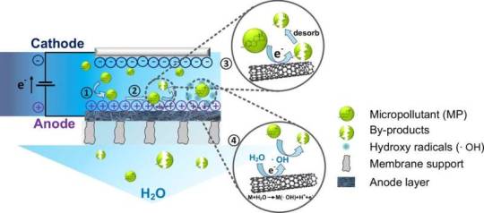
Water treatment: Catching steroid hormones with nanotubes
Steroid hormones are among the most widespread aquatic micropollutants. They are harmful to human health, and they cause ecological imbalances in aquatic environments. At the Karlsruhe Institute of Technology (KIT), researchers have investigated how steroid hormones are degraded in an electrochemical membrane reactor with carbon nanotube membranes. They found that adsorption of steroid hormones on the carbon nanotubes did not limit the hormones' subsequent degradation. Supplying clean water to people around the world is one of the great challenges of today and tomorrow. Various micropollutants (organic and inorganic substances) are present in low concentrations in wastewater but can still be harmful to humans and the environment.
Read more.
#Materials Science#Science#Clean water#Pollutants#Nanotubes#Carbon nanotubes#Nanotechnology#Carbon#Karlsruhe Institute of Technology
43 notes
·
View notes
Text
Carbon Nanotubes: The Miracle Material Revolutionizing Tech, Medicine, and Space Exploration
Carbon nanotubes (CNTs), ultra-strong, lightweight cylinders of carbon atoms, are transforming industries from aerospace to medicine. With 200x the strength of steel and unmatched electrical conductivity, this “wonder material” could redefine the future. Here’s how—and why scientists call it the backbone of 21st-century innovation. 1. What Are Carbon Nanotubes? ⚛️ Atomic Structure Made of…
#advance materials#carbon nanotubes#CNT#Education#EV revolution#future tech#nano materials#nanoscience#nanotechnology#news#news today#research#science#spacetech#technology
0 notes
Video
youtube
Building an Elevator to Outer Space – Adam Brown
0 notes
Text
Making agriculture more resilient to climate change
New Post has been published on https://thedigitalinsider.com/making-agriculture-more-resilient-to-climate-change/
Making agriculture more resilient to climate change
As Earth’s temperature rises, agricultural practices will need to adapt. Droughts will likely become more frequent, and some land may no longer be arable. On top of that is the challenge of feeding an ever-growing population without expanding the production of fertilizer and other agrochemicals, which have a large carbon footprint that is contributing to the overall warming of the planet.
Researchers across MIT are taking on these agricultural challenges from a variety of angles, from engineering plants that sound an alarm when they’re under stress to making seeds more resilient to drought. These types of technologies, and more yet to be devised, will be essential to feed the world’s population as the climate changes.
“After water, the first thing we need is food. In terms of priority, there is water, food, and then everything else. As we are trying to find new strategies to support a world of 10 billion people, it will require us to invent new ways of making food,�� says Benedetto Marelli, an associate professor of civil and environmental engineering at MIT.
Marelli is the director of one of the six missions of the recently launched Climate Project at MIT, which focus on research areas such as decarbonizing industry and building resilient cities. Marelli directs the Wild Cards mission, which aims to identify unconventional solutions that are high-risk and high-reward.
Drawing on expertise from a breadth of fields, MIT is well-positioned to tackle the challenges posed by climate change, Marelli says. “Bringing together our strengths across disciplines, including engineering, processing at scale, biological engineering, and infrastructure engineering, along with humanities, science, and economics, presents a great opportunity.”
Protecting seeds from drought
Marelli, who began his career as a biomedical engineer working on regenerative medicine, is now developing ways to boost crop yields by helping seeds to survive and germinate during drought conditions, or in soil that has been depleted of nutrients. To achieve that, he has devised seed coatings, based on silk and other polymers, that can envelop and nourish seeds during the critical germination process.
A new seed-coating process could facilitate agriculture on marginal arid lands by enabling the seeds to retain any available water.
In healthy soil, plants have access to nitrogen, phosphates, and other nutrients that they need, many of which are supplied by microbes that live in the soil. However, in soil that has suffered from drought or overfarming, these nutrients are lacking. Marelli’s idea was to coat the seeds with a polymer that can be embedded with plant-growth-promoting bacteria that “fix” nitrogen by absorbing it from the air and making it available to plants. The microbes can also make other necessary nutrients available to plants.
For the first generation of the seed coatings, he embedded these microbes in coatings made of silk — a material that he had previously shown can extend the shelf life of produce, meat, and other foods. In his lab at MIT, Marelli has shown that the seed coatings can help germinating plants survive drought, ultraviolet light exposure, and high salinity.
Now, working with researchers at the Mohammed VI Polytechnic University in Morocco, he is adapting the approach to crops native to Morocco, a country that has experienced six consecutive years of drought due a drop in rainfall linked to climate change.
For these studies, the researchers are using a biopolymer coating derived from food waste that can be easily obtained in Morocco, instead of silk.
“We’re working with local communities to extract the biopolymers, to try to have a process that works at scale so that we make materials that work in that specific environment.” Marelli says. “We may come up with an idea here at MIT within a high-resource environment, but then to work there, we need to talk with the local communities, with local stakeholders, and use their own ingenuity and try to match our solution with something that could actually be applied in the local environment.”
Microbes as fertilizers
Whether they are experiencing drought or not, crops grow much better when synthetic fertilizers are applied. Although it’s essential to most farms, applying fertilizer is expensive and has environmental consequences. Most of the world’s fertilizer is produced using the Haber-Bosch process, which converts nitrogen and hydrogen to ammonia at high temperatures and pressures. This energy intensive process accounts for about 1.5 percent of the world’s greenhouse gas emissions, and the transportation required to deliver it to farms around the world adds even more emissions.
Ariel Furst, the Paul M. Cook Career Development Assistant Professor of Chemical Engineering at MIT, is developing a microbial alternative to the Haber-Bosch process. Some farms have experimented with applying nitrogen-fixing bacteria directly to the roots of their crops, which has shown some success. However, the microbes are too delicate to be stored long-term or shipped anywhere, so they must be produced in a bioreactor on the farm.
MIT chemical engineers devised a metal-organic coating that protects bacterial cells from damage without impeding their growth or function.
To overcome those challenges, Furst has developed a way to coat the microbes with a protective shell that prevents them from being destroyed by heat or other stresses. The coating also protects microbes from damage caused by freeze-drying — a process that would make them easier to transport.
The coatings can vary in composition, but they all consist of two components. One is a metal such as iron, manganese, or zinc, and the other is a polyphenol — a type of plant-derived organic compound that includes tannins and other antioxidants. These two components self-assemble into a protective shell that encapsulates bacteria.
Play video
Mighty Microbes: The Power of Protective Polymers
Video: Chemistry Shorts
“These microbes would be delivered with the seeds, so it would remove the need for fertilizing mid-growing. It also reduces the cost and provides more autonomy to the farmers and decreases carbon emissions associated with agriculture,” Furst says. “We think it’ll be a way to make agriculture completely regenerative, so to bring back soil health while also boosting crop yields and the nutrient density of the crops.”
Furst has founded a company called Seia Bio, which is working on commercializing the coated microbes and has begun testing them on farms in Brazil. In her lab, Furst is also working on adapting the approach to coat microbes that can capture carbon dioxide from the atmosphere and turn it into limestone, which helps to raise the soil pH.
“It can help change the pH of soil to stabilize it, while also being a way to effectively perform direct air capture of CO2,” she says. “Right now, farmers may truck in limestone to change the pH of soil, and so you’re creating a lot of emissions to bring something in that microbes can do on their own.”
Distress sensors for plants
Several years ago, Michael Strano, the Carbon P. Dubbs Professor of Chemical Engineering at MIT, began to explore the idea of using plants themselves as sensors that could reveal when they’re in distress. When plants experience drought, attack by pests, or other kinds of stress, they produce hormones and other signaling molecules to defend themselves.
Strano, whose lab specializes in developing tiny sensors for a variety of molecules, wondered if such sensors could be deployed inside plants to pick up those distress signals. To create their sensors, Strano’s lab takes advantage of the special properties of single-walled carbon nanotubes, which emit fluorescent light. By wrapping the tubes with different types of polymers, the sensors can be tuned to detect specific targets, giving off a fluorescent signal when the target is present.
For use in plants, Strano and his colleagues created sensors that could detect signaling molecules such as salicylic acid and hydrogen peroxide. They then showed that these sensors could be inserted into the underside of plant leaves, without harming the plants. Once embedded in the mesophyll of the leaves, the sensors can pick up a variety of signals, which can be read with an infrared camera.
Sensors that detect plant signaling molecules can reveal when crops are experiencing too much light or heat, or attack from insects or microbes.
These sensors can reveal, in real-time, whether a plant is experiencing a variety of stresses. Until now, there hasn’t been a way to get that information fast enough for farmers to act on it.
“What we’re trying to do is make tools that get information into the hands of farmers very quickly, fast enough for them to make adaptive decisions that can increase yield,” Strano says. “We’re in the middle of a revolution of really understanding the way in which plants internally communicate and communicate with other plants.”
This kind of sensing could be deployed in fields, where it could help farmers respond more quickly to drought and other stresses, or in greenhouses, vertical farms, and other types of indoor farms that use technology to grow crops in a controlled environment.
Much of Strano’s work in this area has been conducted with the support of the U.S. Department of Agriculture (USDA) and as part of the Disruptive and Sustainable Technologies for Agricultural Precision (DiSTAP) program at the Singapore-MIT Alliance for Research and Technology (SMART), and sensors have been deployed in tests in crops at a controlled environment farm in Singapore called Growy.
“The same basic kinds of tools can help detect problems in open field agriculture or in controlled environment agriculture,” Strano says. “They both suffer from the same problem, which is that the farmers get information too late to prevent yield loss.”
Reducing pesticide use
Pesticides represent another huge financial expense for farmers: Worldwide, farmers spend about $60 billion per year on pesticides. Much of this pesticide ends up accumulating in water and soil, where it can harm many species, including humans. But, without using pesticides, farmers may lose more than half of their crops.
Kripa Varanasi, an MIT professor of mechanical engineering, is working on tools that can help farmers measure how much pesticide is reaching their plants, as well as technologies that can help pesticides adhere to plants more efficiently, reducing the amount that runs off into soil and water.
Varanasi, whose research focuses on interactions between liquid droplets and surfaces, began to think about applying his work to agriculture more than a decade ago, after attending a conference at the USDA. There, he was inspired to begin developing ways to improve the efficiency of pesticide application by optimizing the interactions that occur at leaf surfaces.
“Billions of drops of pesticide are being sprayed on every acre of crop, and only a small fraction is ultimately reaching and staying on target. This seemed to me like a problem that we could help to solve,” he says.
Varanasi and his students began exploring strategies to make drops of pesticide stick to leaves better, instead of bouncing off. They found that if they added polymers with positive and negative charges, the oppositely charged droplets would form a hydrophilic (water-attracting) coating on the leaf surface, which helps the next droplets applied to stick to the leaf.
Graduate student Maher Damak (left) and associate professor of mechanical engineering Kripa K. Varanasi, have found a way to drastically cut down on the amount of pesticide liquid that bounces off plants.
Later, they developed an easier-to-use technology in which a surfactant is added to the pesticide before spraying. When this mixture is sprayed through a special nozzle, it forms tiny droplets that are “cloaked” in surfactant. The surfactant helps the droplets to stick to the leaves within a few milliseconds, without bouncing off.
In 2020, Varanasi and Vishnu Jayaprakash SM ’19, PhD ’22 founded a company called AgZen to commercialize their technologies and get them into the hands of farmers. They incorporated their ideas for improving pesticide adhesion into a product called EnhanceCoverage.
During the testing for this product, they realized that there weren’t any good ways to measure how many of the droplets were staying on the plant. That led them to develop a product known as RealCoverage, which is based on machine vision. It can be attached to any pesticide sprayer and offer real-time feedback on what percentage of the pesticide droplets are sticking to and staying on every leaf.
RealCoverage was used on 65,000 acres of farmland across the United States in 2024, from soybeans in Iowa to cotton in Georgia. Farmers who used the product were able to reduce their pesticide use by 30 to 50 percent, by using the data to optimize delivery and, in some cases, even change what chemicals were sprayed.
He hopes that the EnhanceCoverage product, which is expected to become available in 2025, will help farmers further reduce their pesticide use.
“Our mission here is to help farmers with savings while helping them achieve better yields. We have found a way to do all this while also reducing waste and the amount of chemicals that we put into our atmosphere and into our soils and into our water,” Varanasi says. “This is the MIT approach: to figure out what are the real issues and how to come up with solutions. Now we have a tool and I hope that it’s deployed everywhere and everyone gets the benefit from it.”
#000#2024#Accounts#adhesion#agriculture#air#ammonia#approach#atmosphere#Bacteria#billion#Biological engineering#biopolymers#Brazil#Building#Capture#carbon#Carbon dioxide#carbon emissions#carbon footprint#carbon nanotubes#career#career development#Cells#challenge#change#chemical#Chemical engineering#chemicals#chemistry
0 notes
Text
Cleaner, Greener New Carbon Nanotubes Synthesis Unveiled
Feb 14: In a breakthrough development in Carbon Nanotubes Synthesis science, researchers at the Institute of Advanced Study in Science and Technology (IASST), an autonomous institute of the Department of Science and Technology (DST), Government of India, have unveiled a pioneering method for the synthesis of Carbon Nanotubes (CNTs) directly on glass substrates. This innovative technique,…

View On WordPress
0 notes
Text
Carbon Nanotubes Market – Global Industry Trends, Uses, Applications, Business Analysis, Growth Opportunities, Segmentation, Graph and Forecast Share to 2028
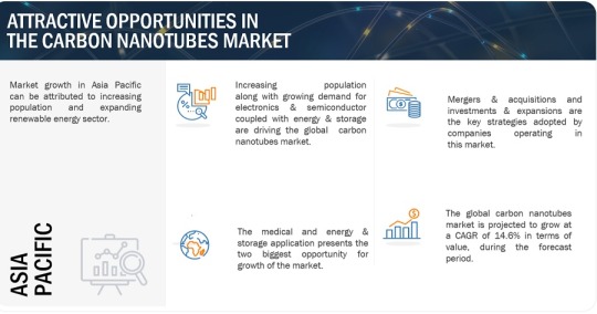
The carbon nanotube (CNT) market exhibits high growth potential and is projected to reach a market size of USD 2.3 billion by 2028 from USD 1.1 billion in 2023, at a CAGR of 14.6%. Asia Pacific is the largest carbon nanotube (CNT) industry that is projected to register the highest CAGR during the forecasted period. This high growth is due to the growing demand from the automotive, electronics &…
View On WordPress
#carbon nanotube applications#carbon nanotube uses#Carbon Nanotubes#Carbon Nanotubes Demand#Carbon Nanotubes Industry#Carbon Nanotubes Industry Trends#Carbon Nanotubes Manufacturers#Carbon Nanotubes Market#Carbon Nanotubes Market Forecast#Carbon Nanotubes Market Graph#Carbon Nanotubes Market Insights#Carbon Nanotubes Market Report#Carbon Nanotubes Market Scope#Carbon Nanotubes Market Trends#cnt applications#cnt uses
0 notes
Text
Carbon Nanotubes and the Sustainability Puzzle
Credit: Katie McKissick, The Kavli FoundationMatteo Pasquali of Rice University discusses unlocking the power of carbon as a sustainable material, replacing conventional, hard-to-decarbonize materials widely used in infrastructure today. Newswise — An international team of researchers receives over $4M to advance understanding of carbon nanotube synthesis and its potential for producing…

View On WordPress
0 notes
Link
0 notes
Text
Starcrete: Paving the Way to a Sustainable Future in Construction
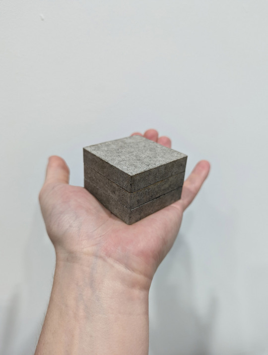
Introduction In the ever-evolving world of construction and infrastructure development, innovation is key to meeting the growing demands of our global population while minimizing environmental impact. One such innovation that holds the promise of revolutionizing the construction industry is “Starcrete.” Starcrete, a groundbreaking material born out of scientific advancements and sustainability…
View On WordPress
#Bridges#Building Sustainability#Carbon Emissions#Carbon Nanotubes#construction industry#construction innovation#Eco-Friendly Material#energy efficiency#environmental benefits#future of construction#Graphene#green building#Green Technologies#infrastructure#infrastructure projects#Recyclable Construction Material#residential construction#Skyscrapers#Starcrete#Sustainable Building Material#Sustainable Construction#Sustainable Development#Technology Advancements
1 note
·
View note
Text
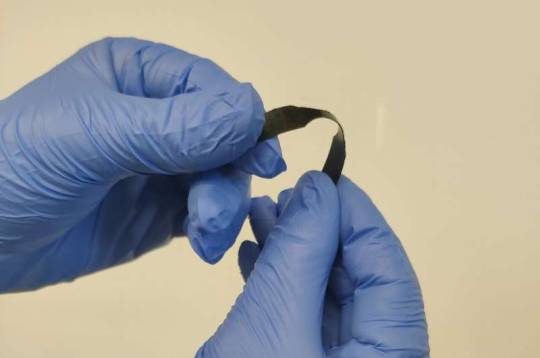
Researchers use carbon nanotube derivatives to strengthen recyclable plastics
Reducing the environmental impact caused by plastics can be addressed through different strategies, such as the manufacture of more durable plastics or recycling. In general, there are two main types of plastics. The first is thermoplastics, which can be melted and molded to form other objects, although their mechanical properties weaken if they are melted several times. And the second, thermosets, do not melt at high temperatures, since the chains of the polymers that form them are intertwined by chemical bonds. Thermoset plastics have advantageous properties compared to thermoplastics. They tend to have a higher resistance to impact and mechanical stress, although they are also more brittle. Epoxy resin, silicone or melamine are examples of thermoset plastics, commonly used in construction. To make these plastics stronger, engineers add reinforcement materials such as carbon fibers. They are already used to manufacture objects such as motorcycle helmets or sports equipment, which are very durable although they cannot be easily recycled.
Read more.
#Materials Science#Science#Carbon nanotubes#Nanotechnology#Carbon#Nanotubes#Plastics#Polymers#Recycling#Strength of materials
23 notes
·
View notes
Text
NCX: Pioneering Carbon Nanotube X-Ray Technology for Precision Imaging
NCX is a premier US-based manufacturer specializing in cold-cathode X-ray sources expertly crafted with cutting-edge carbon nanotube (CNT) technology. We offer a wide range of high-quality X-ray source products to meet the needs of a variety of medical X-ray sources, industrial X-ray sources, and specialty X-ray sources. In addition to our X-ray source products, we also offer a range of solutions and support services to meet the needs of our customers: custom solutions, and technical support. For more information about our innovative products and cutting-edge solutions, please visit our website.
1 note
·
View note
Text

Does the river ever wonder / What will come round the bend? / As it twists and meanders / Down its slow descent
#speci speaks#my art#nms#no man's sky#its hard to tell bit thats carbon nanotubes and wires+microchips in the water#in place of wildflower garlands. yknow. 🥲#idk i thought it was clever. theres also a multitool but if/when i paint this for real i think im gonna leave it out? idk#anyway. artemis ophelia painting#caption is lyrics from 'does the swallow dream of flying' by cosmo sheldrake#WHICH YOU SHOULD LISTEN TO RIGHT NAOW#i maybe shouldve saved the song lyrics caption for if i wanna paint this but i dont Know if i wanna paint it so
13 notes
·
View notes
Text
Thinking about akiha's graphite anon... what a fascinating life...
3 notes
·
View notes
Text
Why can't someone invent a bike that weighs like 2kg and can fit in my backpack
#lmao shut up haz#idk cant we just use carbon nanotubes or something. we live in the 2020s i thot this was the future
2 notes
·
View notes
Text
MIT team takes a major step toward fully 3D-printed active electronics
New Post has been published on https://thedigitalinsider.com/mit-team-takes-a-major-step-toward-fully-3d-printed-active-electronics/
MIT team takes a major step toward fully 3D-printed active electronics
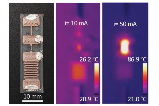

Active electronics — components that can control electrical signals — usually contain semiconductor devices that receive, store, and process information. These components, which must be made in a clean room, require advanced fabrication technology that is not widely available outside a few specialized manufacturing centers.
During the Covid-19 pandemic, the lack of widespread semiconductor fabrication facilities was one cause of a worldwide electronics shortage, which drove up costs for consumers and had implications in everything from economic growth to national defense. The ability to 3D print an entire, active electronic device without the need for semiconductors could bring electronics fabrication to businesses, labs, and homes across the globe.
While this idea is still far off, MIT researchers have taken an important step in that direction by demonstrating fully 3D-printed resettable fuses, which are key components of active electronics that usually require semiconductors.
The researchers’ semiconductor-free devices, which they produced using standard 3D printing hardware and an inexpensive, biodegradable material, can perform the same switching functions as the semiconductor-based transistors used for processing operations in active electronics.
Although still far from achieving the performance of semiconductor transistors, the 3D-printed devices could be used for basic control operations like regulating the speed of an electric motor.
“This technology has real legs. While we cannot compete with silicon as a semiconductor, our idea is not to necessarily replace what is existing, but to push 3D printing technology into uncharted territory. In a nutshell, this is really about democratizing technology. This could allow anyone to create smart hardware far from traditional manufacturing centers,” says Luis Fernando Velásquez-García, a principal research scientist in MIT’s Microsystems Technology Laboratories (MTL) and senior author of a paper describing the devices, which appears in Virtual and Physical Prototyping.
He is joined on the paper by lead author Jorge Cañada, an electrical engineering and computer science graduate student.
An unexpected project
Semiconductors, including silicon, are materials with electrical properties that can be tailored by adding certain impurities. A silicon device can have conductive and insulating regions, depending on how it is engineered. These properties make silicon ideal for producing transistors, which are a basic building block of modern electronics.
However, the researchers didn’t set out to 3D-print semiconductor-free devices that could behave like silicon-based transistors.
This project grew out of another in which they were fabricating magnetic coils using extrusion printing, a process where the printer melts filament and squirts material through a nozzle, fabricating an object layer-by-layer.
They saw an interesting phenomenon in the material they were using, a polymer filament doped with copper nanoparticles.
If they passed a large amount of electric current into the material, it would exhibit a huge spike in resistance but would return to its original level shortly after the current flow stopped.
This property enables engineers to make transistors that can operate as switches, something that is typically only associated with silicon and other semiconductors. Transistors, which switch on and off to process binary data, are used to form logic gates which perform computation.
“We saw that this was something that could help take 3D printing hardware to the next level. It offers a clear way to provide some degree of ‘smart’ to an electronic device,” Velásquez-García says.
The researchers tried to replicate the same phenomenon with other 3D printing filaments, testing polymers doped with carbon, carbon nanotubes, and graphene. In the end, they could not find another printable material that could function as a resettable fuse.
They hypothesize that the copper particles in the material spread out when it is heated by the electric current, which causes a spike in resistance that comes back down when the material cools and the copper particles move closer together. They also think the polymer base of the material changes from crystalline to amorphous when heated, then returns to crystalline when cooled down — a phenomenon known as the polymeric positive temperature coefficient.
“For now, that is our best explanation, but that is not the full answer because that doesn’t explain why it only happened in this combination of materials. We need to do more research, but there is no doubt that this phenomenon is real,” he says.
3D-printing active electronics
The team leveraged the phenomenon to print switches in a single step that could be used to form semiconductor-free logic gates.
The devices are made from thin, 3D-printed traces of the copper-doped polymer. They contain intersecting conductive regions that enable the researchers to regulate the resistance by controlling the voltage fed into the switch.
While the devices did not perform as well as silicon-based transistors, they could be used for simpler control and processing functions, such as turning a motor on and off. Their experiments showed that, even after 4,000 cycles of switching, the devices showed no signs of deterioration.
But there are limits to how small the researchers can make the switches, based on the physics of extrusion printing and the properties of the material. They could print devices that were a few hundred microns, but transistors in state-of-the-art electronics are only few nanometers in diameter.
“The reality is that there are many engineering situations that don’t require the best chips. At the end of the day, all you care about is whether your device can do the task. This technology is able to satisfy a constraint like that,” he says.
However, unlike semiconductor fabrication, their technique uses a biodegradable material and the process uses less energy and produces less waste. The polymer filament could also be doped with other materials, like magnetic microparticles that could enable additional functionalities.
In the future, the researchers want to use this technology to print fully functional electronics. They are striving to fabricate a working magnetic motor using only extrusion 3D printing. They also want to finetune the process so they could build more complex circuits and see how far they can push the performance of these devices.
“This paper demonstrates that active electronic devices can be made using extruded polymeric conductive materials. This technology enables electronics to be built into 3D printed structures. An intriguing application is on-demand 3D printing of mechatronics on board spacecraft,” says Roger Howe, the William E. Ayer Professor of Engineering, Emeritus, at Stanford University, who was not involved with this work.
This work is funded, in part, by Empiriko Corporation.
#000#3-D printing#3d#3D printing#additive manufacturing#Art#author#binary#biodegradable#board#Building#carbon#Carbon materials#carbon nanotubes#chips#computation#computer#Computer Science#consumers#covid#crystalline#data#defense#devices#direction#economic#Electrical engineering and computer science (EECS)#electronic#electronic devices#Electronics
1 note
·
View note
Link
Carbon nanotubes category among the key product segments is expected to be the most promising segment in the global advanced carbon materials market,...
0 notes