#Chip Design
Explore tagged Tumblr posts
Visit Tumblr Blog
Explore Tumblr blogs with no restrictions, modern design and the best experience.
Last Seen Tumblr Blogs


Fun Fact
Tumblr has 4 main sources of revenue.
Text
Industry First: UCIe Optical Chiplet Unveiled by Ayar Labs
New Post has been published on https://thedigitalinsider.com/industry-first-ucie-optical-chiplet-unveiled-by-ayar-labs/
Industry First: UCIe Optical Chiplet Unveiled by Ayar Labs

Ayar Labs has unveiled the industry’s first Universal Chiplet Interconnect Express (UCIe) optical interconnect chiplet, designed specifically to maximize AI infrastructure performance and efficiency while reducing latency and power consumption for large-scale AI workloads.
This breakthrough will help address the increasing demands of advanced computing architectures, especially as AI systems continue to scale. By incorporating a UCIe electrical interface, the new chiplet is designed to eliminate data bottlenecks while enabling seamless integration with chips from different vendors, fostering a more accessible and cost-effective ecosystem for adopting advanced optical technologies.
The chiplet, named TeraPHY™, achieves 8 Tbps bandwidth and is powered by Ayar Labs’ 16-wavelength SuperNova™ light source. This optical interconnect technology aims to overcome the limitations of traditional copper interconnects, particularly for data-intensive AI applications.
“Optical interconnects are needed to solve power density challenges in scale-up AI fabrics,” said Mark Wade, CEO of Ayar Labs.
The integration with the UCIe standard is particularly significant as it allows chiplets from different manufacturers to work together seamlessly. This interoperability is critical for the future of chip design, which is increasingly moving toward multi-vendor, modular approaches.
The UCIe Standard: Creating an Open Chiplet Ecosystem
The UCIe Consortium, which developed the standard, aims to build “an open ecosystem of chiplets for on-package innovations.” Their Universal Chiplet Interconnect Express specification addresses industry demands for more customizable, package-level integration by combining high-performance die-to-die interconnect technology with multi-vendor interoperability.
“The advancement of the UCIe standard marks significant progress toward creating more integrated and efficient AI infrastructure thanks to an ecosystem of interoperable chiplets,” said Dr. Debendra Das Sharma, Chair of the UCIe Consortium.
The standard establishes a universal interconnect at the package level, enabling chip designers to mix and match components from different vendors to create more specialized and efficient systems. The UCIe Consortium recently announced its UCIe 2.0 Specification release, indicating the standard’s continued development and refinement.
Industry Support and Implications
The announcement has garnered strong endorsements from major players in the semiconductor and AI industries, all members of the UCIe Consortium.
Mark Papermaster from AMD emphasized the importance of open standards: “The robust, open and vendor neutral chiplet ecosystem provided by UCIe is critical to meeting the challenge of scaling networking solutions to deliver on the full potential of AI. We’re excited that Ayar Labs is one of the first deployments that leverages the UCIe platform to its full extent.”
This sentiment was echoed by Kevin Soukup from GlobalFoundries, who noted, “As the industry transitions to a chiplet-based approach to system partitioning, the UCIe interface for chiplet-to-chiplet communication is rapidly becoming a de facto standard. We are excited to see Ayar Labs demonstrating the UCIe standard over an optical interface, a pivotal technology for scale-up networks.”
Technical Advantages and Future Applications
The convergence of UCIe and optical interconnects represents a paradigm shift in computing architecture. By combining silicon photonics in a chiplet form factor with the UCIe standard, the technology allows GPUs and other accelerators to “communicate across a wide range of distances, from millimeters to kilometers, while effectively functioning as a single, giant GPU.”
The technology also facilitates Co-Packaged Optics (CPO), with multinational manufacturing company Jabil already showcasing a model featuring Ayar Labs’ light sources capable of “up to a petabit per second of bi-directional bandwidth.” This approach promises greater compute density per rack, enhanced cooling efficiency, and support for hot-swap capability.
“Co-packaged optical (CPO) chiplets are set to transform the way we address data bottlenecks in large-scale AI computing,” said Lucas Tsai from Taiwan Semiconductor Manufacturing Company (TSMC). “The availability of UCIe optical chiplets will foster a strong ecosystem, ultimately driving both broader adoption and continued innovation across the industry.”
Transforming the Future of Computing
As AI workloads continue to grow in complexity and scale, the semiconductor industry is increasingly looking toward chiplet-based architectures as a more flexible and collaborative approach to chip design. Ayar Labs’ introduction of the first UCIe optical chiplet addresses the bandwidth and power consumption challenges that have become bottlenecks for high-performance computing and AI workloads.
The combination of the open UCIe standard with advanced optical interconnect technology promises to revolutionize system-level integration and drive the future of scalable, efficient computing infrastructure, particularly for the demanding requirements of next-generation AI systems.
The strong industry support for this development indicates the potential for a rapidly expanding ecosystem of UCIe-compatible technologies, which could accelerate innovation across the semiconductor industry while making advanced optical interconnect solutions more widely available and cost-effective.
#accelerators#adoption#ai#AI chips#AI Infrastructure#AI systems#amd#Announcements#applications#approach#architecture#bi#CEO#challenge#chip#Chip Design#chips#collaborative#communication#complexity#computing#cooling#data#Design#designers#development#driving#efficiency#express#factor
2 notes
·
View notes
Text
3 notes
·
View notes
Text
youtube
Use this trick to Save time : HDL Simulation through defining clock
Why is this trick useful? Defining a clock in your simulation can save you time during simulation because you don't have to manually generate the clock signal in your simulation environment. Wanted to know how to define and force clock to simulate your digital system. Normally define clock used to simulate system with clock input. But I am telling you this trick for giving values to input ports other than clock. It will help you to save time in simulation because you do not need to force values to input ports every time. Lets brief What we did - gave some clock frequency to input A, like we gave 100. Than we made Half the frequency of clock to 50 and gave it to Input B. In similar way if we have 3rd input too we goanna half the frequency again to 25 and would give to next input.
Subscribe to "Learn And Grow Community"
YouTube : https://www.youtube.com/@LearnAndGrowCommunity
LinkedIn Group : https://www.linkedin.com/groups/7478922/
Blog : https://LearnAndGrowCommunity.blogspot.com/
Facebook : https://www.facebook.com/JoinLearnAndGrowCommunity/
Twitter Handle : https://twitter.com/LNG_Community
DailyMotion : https://www.dailymotion.com/LearnAndGrowCommunity
Instagram Handle : https://www.instagram.com/LearnAndGrowCommunity/
Follow #LearnAndGrowCommunity
#HDL Design#Digital Design#Verilog#VHDL#FPGA#Digital Logic#Project#Simulation#Verification#Synthesis#B.Tech#Engineering#Tutorial#Embedded Systesm#VLSI#Chip Design#Training Courses#Software#Windows#Certification#Career#Hardware Design#Circuit Design#Programming#Electronics Design#ASIC#Xilinx#Altera#Engineering Projects#Engineering Training Program
2 notes
·
View notes
Text
🚀 Big news! Apple has unveiled its first custom-designed C1 modem chip, marking a significant leap in wireless technology. Say goodbye to Qualcomm reliance and hello to improved connectivity and battery life! 🌐✨ #Apple #C1Modem #WirelessTechnology #iPhone16e
#Apple#battery life#C1 modem chip#chip design#iPhone 16e#Qualcomm#smartphone connectivity#wireless technology
0 notes
Text
Empowering Embedded Software and Semiconductor Design in the USA
Embedded systems and semiconductor technology have converged, paving the way for a transformative future that reshapes our interactions with the world. The semiconductor industry's continuous innovation and turnkey chip design empower custom solutions, ushering in an exciting era of technological breakthroughs. At ACL Digital, we meet the demands for high performance, complexity, cost-effectiveness, and reliable hardware and software components for OEMs and Enterprises alike.

Your Partner in Embedded Software Solutions and Services
At ACL Digital, we offer a full spectrum of services in chip design and embedded software solutions in the USA. From architecture to RTL design, verification, and GDSII, our engineering team leads innovation, designing cutting-edge chips that meet rapid development demands and industry scalability. Our focus on low power, high speed, and area-efficient designs allows us to deliver advanced solutions globally.
Key Highlights of Our Semiconductor Practice
Comprehensive Capabilities
We build next-generation semiconductor solutions, from initial chip design to advanced silicon and embedded software, driven by constant innovation and technical expertise.
Integrated Design and Testing
Our seamless integration of design and test engineering processes enables customers to develop new solutions with optimized costs and maximized performance.
Our Offerings
VLSI Design and Engineering
Elevate your projects with our advanced VLSI solutions. Our experts provide unmatched technological excellence in delivering top-of-the-line solutions for your unique requirements.
Silicon Embedded Engineering
Empower your innovations with comprehensive silicon-embedded engineering capabilities. We offer services from pre-silicon to post-silicon validation, solution engineering, pro-support/IDH, and more.
Why Choose ACL Digital?
Pioneering Expertise
We lead in design-led Semiconductor Engineering, Product Engineering, and Digital Experience Services.
Strong Technology Partnerships
We partner with leading semiconductor companies like NXP, Marvell, Texas Instruments, Silicon Labs, and ARM to provide complete development cycle support.
Technological Advancements
Stay ahead with early access to cutting-edge platforms. Our clients gain a competitive edge by leveraging our market readiness.
Centers of Excellence (CoEs)
Expertise in RISC-V, ARM, TSMC, and Functional Safety (FuSa) ensures that we meet the highest standards of performance, reliability, and security.
Advanced Technology Expertise
We deliver semiconductor design services, including SoC system blocks, CPU subsystems, high-speed IOs, low-speed IOs, and analog/mixed-signal designs.
Industry Leadership
As a dependable go-to partner, we cater to projects ranging from pre-silicon and platform software to solution engineering and technical support, ensuring unparalleled excellence in every aspect of your semiconductor journey.
Discover the potential of embedded systems and semiconductor solutions in the USA with ACL Digital. Our dedication to innovation and excellence ensures that we deliver the best-in-class solutions to all our customers. Contact us today to learn how we can transform your technology landscape.
0 notes
Text
TF One Bumblebee as TFP Bumblebee? why not
[Please do not steal, trace, repost or modify my work]
#orionsart#I swapped out bulkhead for ironhide#and Knockout gets his own design i made up#anyway take this silly little animatic as we wait for my other 2 projects ToT#sorry the d-16 animatic is taking a while school has been kicking my ass#but i am chipping away at it little by little… trust 🙏🏼#transformers#bumblebee#transformers one#b 127#artists on tumblr#maccadam#knockout#knockout tfp#transformers prime#tfp#tf one#transformers fanart#small artist#art
2K notes
·
View notes
Note
Final manifestations for Book 7?
I'm trying REALLY hard not to build up any solid expectations, because I wanna go in ~fresh~! they're already so far away from anything I thought would happen (not in a bad way, I'm just accepting that I'm on Miss Yana's Wild Ride at this point and we're seeing this thing through 'til the end, by gum). so it's nothing too major, but:
they've been handing new crying expressions out like candy lately, I want to see some delicious Malleus tears.
honestly I want everyone to cry buckets. their tears sustain me. the more Silver angst specifically I get the happier I am.
SILVER!!!! 👏 VANROUGE!!!! 👏
just let him have this. the poor boy's been through so much. let him have his big "I'm proud of you, son" moment with Lilia.
I'm 100% expecting Grim's arc (and probably whatever's going on with Crowley) to be its own episode, but a nice hook to leave us hanging on would be good!
a nice hook though, please, I don't think I can take another "Grim is attacking us! now wait eight months to find out what happens :)" cliffhanger...
some Meleanor? as a treat? just a little bit, a tiny quick flashback or something, please Twst I just, I just want to see her again. let her have a little ghost cameo like Dawnathan Knight got. Lilia and his kids are all having their big group hug or whatever and she can gently fade in to be all like

(turning asks off until I'm done playing, SEE YOU ON THE OTHER SIDE Y'ALL)
#art#twisted wonderland#twisted wonderland spoilers#twisted wonderland episode 7 spoilers#twisted wonderland book 7 spoilers#twisted wonderland episode 7 part 13 spoilers#twisted wonderland book 7 part 13 spoilers#one last chance for me to be wrong about everything!#(no it's good i am enjoying it SO much) (just stomping right down on all of my personal like buttons with its whole weight)#(it's just also VERY good at totally subverting all of my expectations)#i don't think we're actually gonna get a permanently dehorned malleus though#just because it feels like an insane thing to remove the most iconic part of one of the most iconic characters of the game#but i could see like...a temporary thing ala raisin vil#or a permanent smaller change like cracks/chips or something (kintsugi horns would be super cool actually)#but i do think it's more likely we'll find some way to keep the status quo re:horn design#if this was the END-end of all of twst then maybe but they still wanna sell merch of this guy so they can't change his design TOO much#i am sorta wondering if he might get a bit of a power nerf though? take him down from ridiculously overpowered to just normal overpowered#idk they made a point of saying the horns were specifically what caused the weather stuff#and the weather stuff has been called out in particular as one of the reasons why mal being so stupidly magical makes him pretty unhappy#everyone's scared of him all the time and he has to actively try not to accidentally kill people when he gets upset#so. idk. maybe it was just a little worldbuilding. but i thought it was interesting they brought that up was all!#me: i'm not going to form any expectations (writes a whole thing speculating on the fate of malleus' horns)#look it's now or never okay#that end of episode rhythmic better be SO cute because i'm already losing my entire head over this
2K notes
·
View notes
Text


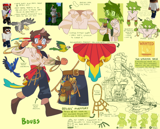
ETHO - BDUBS - GEM Designs for Season 10!
They be pirates :]
Every new smp/series I come across- i like to assign an overarching theme to it and this hc season is no different:
The mainland of Season 10 is riddled with pirates and cowboys. Each hermit is wanted of some charge, for one reason or another. As initiation, losing a life will remove that bounty and that hermit can start fresh. But becoming the last survivor, that hermit will be gifted the Treasure of the Island (whatever the reward Grian says it is 😭)
#stufffsart#character concept stufff#geminitay#etho#ethoslab#bdoubleo100#bdoubleo#Bdubs#hermitcraft#hermitcraft season 10#hermitblr#mcytblr#been wanting to put more meaning into my design choices and explaining it :]#been chipping away at this since day 2 of the server it just kept going and going..
5K notes
·
View notes
Note
67?


(ID in ALT text) i know technically this can't be considered a wip. but it is wip to me because to this day i can't still pick ONE to post and i keep going back and forth.. and so it got doomed to stay in my folders just like this?
#chip!ask#wip ask game#yue#tui!yue#designing outfits is fun!#until you have multiple favourites....#and then you can't pick a favourite...
4K notes
·
View notes
Text


POV: you’re jay and you just wanted a midnight snack
#solar beams art atcha#jrwi riptide#jrwi fanart#jrwi#chip jrwi#jrwi gillion#jrwi fnc#fish and chips#ig?#I just drew this to memorize their designs
462 notes
·
View notes
Text
MIT engineers grow “high-rise” 3D chips
New Post has been published on https://thedigitalinsider.com/mit-engineers-grow-high-rise-3d-chips/
MIT engineers grow “high-rise” 3D chips
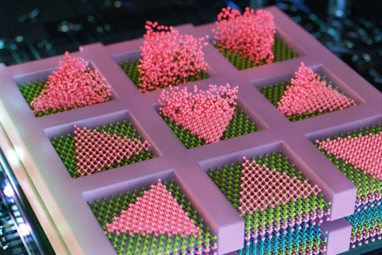
The electronics industry is approaching a limit to the number of transistors that can be packed onto the surface of a computer chip. So, chip manufacturers are looking to build up rather than out.
Instead of squeezing ever-smaller transistors onto a single surface, the industry is aiming to stack multiple surfaces of transistors and semiconducting elements — akin to turning a ranch house into a high-rise. Such multilayered chips could handle exponentially more data and carry out many more complex functions than today’s electronics.
A significant hurdle, however, is the platform on which chips are built. Today, bulky silicon wafers serve as the main scaffold on which high-quality, single-crystalline semiconducting elements are grown. Any stackable chip would have to include thick silicon “flooring” as part of each layer, slowing down any communication between functional semiconducting layers.
Now, MIT engineers have found a way around this hurdle, with a multilayered chip design that doesn’t require any silicon wafer substrates and works at temperatures low enough to preserve the underlying layer’s circuitry.
In a study appearing today in the journal Nature, the team reports using the new method to fabricate a multilayered chip with alternating layers of high-quality semiconducting material grown directly on top of each other.
The method enables engineers to build high-performance transistors and memory and logic elements on any random crystalline surface — not just on the bulky crystal scaffold of silicon wafers. Without these thick silicon substrates, multiple semiconducting layers can be in more direct contact, leading to better and faster communication and computation between layers, the researchers say.
The researchers envision that the method could be used to build AI hardware, in the form of stacked chips for laptops or wearable devices, that would be as fast and powerful as today’s supercomputers and could store huge amounts of data on par with physical data centers.
“This breakthrough opens up enormous potential for the semiconductor industry, allowing chips to be stacked without traditional limitations,” says study author Jeehwan Kim, associate professor of mechanical engineering at MIT. “This could lead to orders-of-magnitude improvements in computing power for applications in AI, logic, and memory.”
The study’s MIT co-authors include first author Ki Seok Kim, Seunghwan Seo, Doyoon Lee, Jung-El Ryu, Jekyung Kim, Jun Min Suh, June-chul Shin, Min-Kyu Song, Jin Feng, and Sangho Lee, along with collaborators from Samsung Advanced Institute of Technology, Sungkyunkwan University in South Korea, and the University of Texas at Dallas.
Seed pockets
In 2023, Kim’s group reported that they developed a method to grow high-quality semiconducting materials on amorphous surfaces, similar to the diverse topography of semiconducting circuitry on finished chips. The material that they grew was a type of 2D material known as transition-metal dichalcogenides, or TMDs, considered a promising successor to silicon for fabricating smaller, high-performance transistors. Such 2D materials can maintain their semiconducting properties even at scales as small as a single atom, whereas silicon’s performance sharply degrades.
In their previous work, the team grew TMDs on silicon wafers with amorphous coatings, as well as over existing TMDs. To encourage atoms to arrange themselves into high-quality single-crystalline form, rather than in random, polycrystalline disorder, Kim and his colleagues first covered a silicon wafer in a very thin film, or “mask” of silicon dioxide, which they patterned with tiny openings, or pockets. They then flowed a gas of atoms over the mask and found that atoms settled into the pockets as “seeds.” The pockets confined the seeds to grow in regular, single-crystalline patterns.
But at the time, the method only worked at around 900 degrees Celsius.
“You have to grow this single-crystalline material below 400 Celsius, otherwise the underlying circuitry is completely cooked and ruined,” Kim says. “So, our homework was, we had to do a similar technique at temperatures lower than 400 Celsius. If we could do that, the impact would be substantial.”
Building up
In their new work, Kim and his colleagues looked to fine-tune their method in order to grow single-crystalline 2D materials at temperatures low enough to preserve any underlying circuitry. They found a surprisingly simple solution in metallurgy — the science and craft of metal production. When metallurgists pour molten metal into a mold, the liquid slowly “nucleates,” or forms grains that grow and merge into a regularly patterned crystal that hardens into solid form. Metallurgists have found that this nucleation occurs most readily at the edges of a mold into which liquid metal is poured.
“It’s known that nucleating at the edges requires less energy — and heat,” Kim says. “So we borrowed this concept from metallurgy to utilize for future AI hardware.”
The team looked to grow single-crystalline TMDs on a silicon wafer that already has been fabricated with transistor circuitry. They first covered the circuitry with a mask of silicon dioxide, just as in their previous work. They then deposited “seeds” of TMD at the edges of each of the mask’s pockets and found that these edge seeds grew into single-crystalline material at temperatures as low as 380 degrees Celsius, compared to seeds that started growing in the center, away from the edges of each pocket, which required higher temperatures to form single-crystalline material.
Going a step further, the researchers used the new method to fabricate a multilayered chip with alternating layers of two different TMDs — molybdenum disulfide, a promising material candidate for fabricating n-type transistors; and tungsten diselenide, a material that has potential for being made into p-type transistors. Both p- and n-type transistors are the electronic building blocks for carrying out any logic operation. The team was able to grow both materials in single-crystalline form, directly on top of each other, without requiring any intermediate silicon wafers. Kim says the method will effectively double the density of a chip’s semiconducting elements, and particularly, metal-oxide semiconductor (CMOS), which is a basic building block of a modern logic circuitry.
“A product realized by our technique is not only a 3D logic chip but also 3D memory and their combinations,” Kim says. “With our growth-based monolithic 3D method, you could grow tens to hundreds of logic and memory layers, right on top of each other, and they would be able to communicate very well.”
“Conventional 3D chips have been fabricated with silicon wafers in-between, by drilling holes through the wafer — a process which limits the number of stacked layers, vertical alignment resolution, and yields,” first author Kiseok Kim adds. “Our growth-based method addresses all of those issues at once.”
To commercialize their stackable chip design further, Kim has recently spun off a company, FS2 (Future Semiconductor 2D materials).
“We so far show a concept at a small-scale device arrays,” he says. “The next step is scaling up to show professional AI chip operation.”
This research is supported, in part, by Samsung Advanced Institute of Technology and the U.S. Air Force Office of Scientific Research.
#2-D#2023#2D materials#3d#ai#AI chip#air#air force#applications#Arrays#Artificial Intelligence#atom#atoms#author#Building#chip#Chip Design#chips#coatings#communication#computation#computer#computer chips#computing#craft#crystal#crystalline#data#Data Centers#Design
2 notes
·
View notes
Text
1 note
·
View note
Text

my piece for the jrwi twitter secret santa for @/aceischaotic on twitter! this is the first art secret santa I’ve done and I had a great time making it, I definitely want to do more in the future.
#just roll with it#jrwi fanart#jrwi riptide#jrwi chip#jrwi gillion#jrwi jay#this was my first time drawing jay surprisingly#i really need to come up with designs for all three so i’m not having to follow canon so strictly#unfortunately im just extremely indecisive#my art
449 notes
·
View notes
Text
ACL Digital is Your Preferred Partner for Semiconductor Solutions in the USA

Embedded systems and semiconductor technology have converged, reshaping our interactions with the world. Continuous innovation in the semiconductor industry is driving technological breakthroughs, creating a more innovative, highly connected world. ACL Digital provides high-performance, cost-effective, and reliable hardware and software solutions for OEMs and enterprises.
Comprehensive Semiconductor Services in the USA
ACL Digital empowers your chip design journey with a full spectrum of services, including VLSI IPs, ASICs, SoCs, and FPGAs. From architecture to RTL design, verification, and GDSII, our engineering team is at the forefront of innovation. We focus on low-power, high-speed, and area-efficient designs to deliver advanced solutions globally.
Key Highlights of Our Semiconductor Practice
In-House Capabilities
We build next-generation semiconductor solutions in the USA, from initial chip design to cutting-edge silicon and embedded software.
Seamless Integration
Our design and test engineering processes enable optimized costs and maximized performance.
End-to-End Services
We offer chip design, verification, IP integration, and embedded software solutions, ensuring the highest ROI on R&D investments.
ACL Digital’s Semiconductor Offerings
VLSI Design and Engineering
Advanced VLSI solutions and engineering expertise, from RTL design and architecture to FIP.
Silicon Embedded Engineering
Comprehensive services from pre-silicon to post-silicon validation, solution engineering, pro-support/IDH, and more.
Why Choose ACL Digital
Expert in Semiconductor Solutions
We lead in design-led semiconductor engineering, product engineering, and digital experience services.
Strong Technology Partnerships
Collaborations with NXP, Marvell, Texas Instruments, Silicon Labs, ARM, and others provide full development cycle support.
Technological Advancements
Market readiness and early access to cutting-edge platforms give our clients a competitive edge.
Centers of Excellence (CoEs)
Expertise in RISC-V, ARM, TSMC, and Functional Safety (FuSa) ensures cutting-edge design solutions.
Advanced Technology Expertise
Deep understanding of SoC system blocks, CPU subsystems, high-speed IOs, low-speed IOs, and analog/mixed-signal designs.
Industry Expert
Trusted partner for pre-silicon, platform software, and solution engineering, providing unwavering technical support.
ACL Digital stands out among semiconductor chip design companies, offering top-tier semiconductor solutions and semiconductor services in the USA. You can partner with us to navigate the complexities of the semiconductor industry and drive your technological advancements forward.
Contact Us Today
Discover how ACL Digital can elevate your semiconductor solutions in the USA. Contact us to learn more about our services and how we can help you achieve your goals.
0 notes
Text

gillgillgillgillgillgillgillgillgillgillgillgillgillgillgillgillgillgillgillgillgillgillgillgill
#caption is my best ep32 drunk chip impression#hes so on my mind#hes so in my head#hes so hes hes hes soooooo#i dont think i will ever stop fiddling with their designs. doubly so bc they change over the course of the story too...#so many looks to keep in my head... oaughh#just roll with it#jrwi riptide#gillion tidestrider#jrwi pretzel#my art#idk why the pose is like that uh it wasnt supposed to turn into this whole thing but yknow :)#i will.... maybe. draw him with his armor... one day.. sometime in the future...
2K notes
·
View notes
Text


FINALLY RELEASING MAGICAL GIRL ALBATRIO UPON THE WORLD 🎉🎉 worked on these for @vyrion's madoka au, go check it out
#jrwi#just roll with it#jrwi riptide#jay ferin#jrwi chip#gillion tidestrider#madoka au#magical girl au#avepharts#this has been in the works for MONTHS so please go show vyrion some support if you're interested#ive had so much fun working on it also. character design my love my life.#also accidentally deleted and had to rewrite the jay id dont look at me.
1K notes
·
View notes