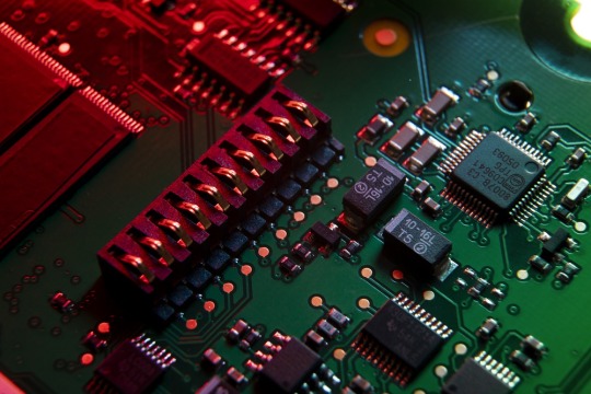
#can transceiver circuit
Explore tagged Tumblr posts
Visit Tumblr Blog
Explore Tumblr blogs with no restrictions, modern design and the best experience.
Last Seen Tumblr Blogs


Fun Fact
Users from the US are the majority of Tumblr visitors.
Text
https://www.futureelectronics.com/p/semiconductors--comm-products--can/mcp2551t-i-sn-microchip-5971353
High-Speed CAN Transceiver, can transceiver circuit, Can Power Systems
MCP2551 Series 5.5 V 1 Mb/s Surface Mount High-Speed CAN Transceiver - SOIC-8
#Microchip#MCP2551T-I/SN#Comm Products#CAN#High-Speed CAN Transceiver#can transceiver circuit#Can Power Systems#Can controller#can bus#can bus voltage#Can bus voltage measurement#Embedded communication
1 note
·
View note
Text
https://www.futureelectronics.com/p/semiconductors--comm-products--phy/ksz8721bli-microchip-6275010
High-Speed CAN Transceiver, ethernet PHY chip, Ethernet controller
KSZ8721B Series 2.5 V 10/100 Base TX/FX Physical Layer Transceiver - LQFP-48
#Comm Products#PHY#KSZ8721BL#Microchip#High-Speed CAN Transceiver#ethernet PHY chip#Ethernet controller#Ethernet MAC controller#communications products#electronic circuit#Physical Layer Transceiver#physical layer
1 note
·
View note
Text
Mechismo - No. 03 /// Speak
(First) / (Previous)
When the reappropriated battle-radio crackles to life— Pss-Tat-tat. It’s good.
“—ou copy? Answer! I know—” Psssat-at-at. It’s the oft-heard, impatient snap of takeout breadstick or asshole-bone. Psst-tat. One of those, at least. “—need help.
Okay?”
Boots slip to the deck in a restrained show of attentiveness; pulled through loose cablets — anxiously-chewed at the stray ends — that have hewn radio to emplaced console. That beg it remain connected, to the dropship’s comm-booster. Tsss-at-tat. Still within reach.
You want to hear this — need to, were waiting to.
But the pack — lance, she’ll be here soon to pipe-in indignant with — doesn’t need to see that, their breaths hitching as you click down on the transceiver, “Aww. Howdy pup, ya not doin’ so good right now?”
“Don’t call— Ugh. You were right!” she exclaims. “Not—” Psss— Tick!
Tsss-Tick-tick! The radio needs to be tuned to hers — its signal obfuscated before now, even with the leash hardwired between them, and the tracker buried in her bought-out frame.
It’s the hiss-click when internal-atmos sneers out through a cockpit-shield; where— Tsss-Tick! Where the sea presses on its laminate interlace which melds still, after hours sunken, the internal-external halves of its shattered, protective screen into purposed form.
Whereon the seabed her mech rests to be recovered, and indebted for the courtesy.
Tick-tsss-tick. Or the kettle that rattles to a whinesome, third climax — another pack-hound ordered to bring her tea, without notice to the possibility it’s because it never tastes how she made it. Tsss-tick-Tick-Tick!
One of those,
at least.
It takes some more dials to find her. Tick-tick—Tack! Then it locks in, and she’s yours.
“—were knocked out. So it’s just me — that’s left,” she pleads between the hiss that remains: the unmistakable whine of pilot exhaustion and shrapnel-bled coolant dripping onto wet, fizzing circuits. “Okay.”
Somewhere below, a treat rattles from tread-to-tread; out of the recesses of bounced-up combat boots, through metal slats into the underdeck — for the rats, not dogs, to feast on this time. Though one still mounts a boot-tip, bobs up into your spare hand, and “Oh. How I’d just adore making it all right for ya pup,” you drawl, wait out the seconds, to lap up each transceived pant of desperation. “But— y’know, ya gotta make it right first.”
Speakers shudder in electric anticipation as the meagre band of frequencies a battle-radio is allowed to occupy choke on two shots in sudden succession. Thhunkh. Thunkhh. Your radar flickers into range, to see the targeted blips but a moment before they flicker out.
There’s so many more than those ones, than hers — bright speckles of seawater mould on the dull, hooded monitor.
“Yeah. Sure,” she spills, spent shells in the oil-suckered muck, doesn’t have the time to mute, “can take it from my friends’ corpses when this contract’s done — like I didn’t pay enough gettin’ outta yours.”
You think it’s a shame, how she values them — valued them — over her own family, slipping her leash to leave the pack behind. “Handler,” she begs — her words huddled between the rhythmic shunts of her main-arm reloading.
You feel the way it tears itself apart each time it fires — how it trades off: so much power, but it must hurt itself too. How she didn’t know how to repair it — before you, “No.”
“Wha—”
“No more debts,” you append, in correction of her. It’d look the same on the company files but, “Ya always looked sad when ya owed me.”
“So how the fuck am I supposed to—” Her shriek suffers another’s interjection; the hull-creasing bellow of another blow taken, less glanced than the last, less her fainting gesture at leverage. “Fine! You wanna fuck me, right? ‘Cos I never gave you the chance.”
Mould pours into a brittle crescent around her, cut apart at the gridlines and nowhere else.
She must’ve backed into her prize: a vessel downed in distant memory, too much promise of precious relics to be uncontested, now the winds have shaken it from its grave. At last its rusted silvered shell bounces an invisible laser back into the rangefinder. You count down each point: two-point-six clicks, two-point-five, point-four, point-three.
She doesn’t need to know that — would know it herself,
“Ya ain’t gotta make it right to me,” you explain, punctuate it with the loose, separation-anxious howl of the smallest of the pack’s three. It nuzzles past the mounted one, and whimpers as you tamp fingers down on radio and tongue, to tell her.
“It’s to your sisters.”
All your hounds whine now, except her. But that’s still good. The pilot-suits will recirculate the lost fluid — most of it. The rest will help it slip off, after she’s back, and even before that it’s little between them and the ridged, rubber toe-caps each vies to press themselves into.
“Are you not over this,” she cries, even though it’ll soak the soft trim of her head-mounted display. “I left months ago and I’m dying now.”
You retreat a wet index-finger from an eager, pulsing throat — rub the mess on its cheek, let out a soft snap. “I’m not, pup,” you turn on her, and two sub-point clicks fly past before you’re able to continue, “and you're already whining so perfectly for me.”
Each hound has stirred now, rushing to collar themselves in their owned, metal skin.
Your words echo into their cockpits, “Bark for your owner.”
It’s not even for them but— Awooo! And it must count sixty-four seconds or less, till they’re hot and grounded, “and I’ll be right over.”
If they want their reward, “I can’t believe I’m—” If there’s still one to collect.
You look at that speckled crescent, know from how it falls on her what each wretched speckle is — model, armament, pilot-temperament — and can count the seconds you’ll need to break it. Can count the second you have to break it, and are losing as drop-sirens howl and steel starts to pounce upon the earth.
“Daisy,” you bark — worried she’s silent.
But then, the radio crackles. You hear the hitch in her throat — as the dropship shadows the broken field, before her pack lights the darkness, and realise, in relief, that she is waiting — waiting to, “Speak!”
“Arf!”
“Good girl.”
---
(Masterpost) / (Next)
written for Making-up-Mech-Pilots' prompt:
Mech Pilot who is very upset that they don't get to pick their own callsign.
technically started writing this before i made a tumblr account but i believe this will be appreciated here. it started off more playful and invariably i have made it sad but also smutty. lmk if you like it <3
#4 minute read#melino�� writes#mech pilot#mechposting#mecha#dollposting#f/f#standalone fic#short story#puppygirl#this one is for the puppygirls#it was less sad when i started writing it#mechismo
30 notes
·
View notes
Text
———
[Attached: a short video. It’s from the perspective of the X-transceiver tied around August’s wrist. From the way the camera’s moving, you can assume she’s running her hands up and down either of her arms. You hear her teeth clatter as she walks through a door with an obnoxious star-shaped sign hanging on the front, and enters one of the dressing rooms of Pokéstar Studios.
He walks over to the desk on the far side of the room, and lets out a sigh of relief when he finds his laptop beneath a few stacks of makeup containers. As he pushes them off and picks up his computer, you catch a glimpse of something growing up his trembling arm…
It doesn’t go unnoticed by August, either. He lifts both his arms up, and you see in the mirror his horrified and confused expression as he watches a thin layer of frost travel up the lengths of his arm.
“Wh-wh-what th-the…?”
The video ends when the frost reaches their wrist, traveling over the camera of their X-transceiver and causing the device to short-circuit.]
———
#frozen over arc#pkmn irl#pkmn rp#pokeblog rp#pokeblogging#pokeirl#pokemon irl#pokemon rp#trainer august#pokemon
5 notes
·
View notes
Text
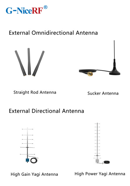
Best Partner for Wireless Modules: A Comprehensive Antenna Selection Guide
n the field of wireless communication, antenna selection is crucial. It not only affects the coverage range and transmission quality of signals but also directly relates to the overall performance of the system. Among various wireless modules, finding the right antenna can maximize their potential, ensuring stable and efficient data transmission.
When designing wireless transceiver devices for RF systems, antenna design and selection are essential components. A high-quality antenna system can ensure optimal communication distances. Typically, the size of antennas of the same type is proportional to the wavelength of the RF signal; as signal strength increases, the number of required antennas also grows.
Antennae can be categorized as internal or external based on their installation location. Internal antennas are installed within the device, while external antennas are mounted outside.
In situations where space is limited or there are multiple frequency bands, antenna design becomes more complex. External antennas are usually standard products, allowing users to simply select the required frequency band without needing additional tuning, making them convenient and easy to use.
What are the main types of antennas?
External Antennas: These antennas can be classified into omnidirectional antennas and directional antennas based on the radiation pattern.
Internal Antennas: These antennas refer to antennas that can be placed inside devices.
Omnidirectional Antennas: These antennas radiate signals uniformly in the horizontal plane, making them suitable for applications that require 360-degree coverage, such as home Wi-Fi routers and mobile devices.
Directional Antennas: These antennas have a high emission and reception strength in one or more specific directions, while the strength is minimal or zero in others. Directional antennas are primarily used to enhance signal strength and improve interference resistance.
PCB Antennas: These antennas are directly printed on the circuit board and are suitable for devices with limited space, commonly used in small wireless modules and IoT devices.
FPC Antennas: FPC antennas are flexible printed circuit antennas that are lightweight, efficient, and easy to integrate.
Concealed Antennas: Designed for aesthetic purposes, concealed antennas can be hidden within devices or disguised as other objects, making them suitable for applications where appearance is important without compromising signal quality.
Antenna Selection Guide
When selecting the appropriate antenna for a communication module, it's essential to first determine whether to use an internal or external antenna based on the module's structure.

External Antennas: These antennas offer high gain, are less affected by the environment, and can save development time, but they may take up space and impact the product's aesthetics.
Internal Antennas: These have relatively high gain and are installed within the device, maintaining a clean and appealing exterior.
Sucker Antennas: These provide high gain and are easy to install and secure.
Copper Rod Sucker Antennas: Made from large-diameter pure copper radiators, these are highly efficient with a wide bandwidth.
Rubber Rod Antennas: Offer moderate gain at a low cost.
Fiberglass Antennas: Suitable for harsh environments and ideal for long-distance signal

External Directional Antennas
Typically used in environments with long communication distances, small signal coverage areas, and high target density.
Panel Antennas have high efficiency, are compact, and easy to install, while considering the impact of gain and radiation area Yagi Antennas offer very high gain, are slightly larger, and have strong directionality, making them suitable for long-distance signal transmission; however, attention must be paid to the antenna's orientation during use
Internal Antenna Selection
Most internal antennas are affected by environmental factors and may require custom design or impedance matching
Spring Antennas are cost-effective but have low gain and narrow bandwidth, often requiring tuning for good matching when installed Ceramic Patch Antennas occupy minimal space and perform well, but have a narrow bandwidth
For details, please click:https://www.nicerf.com/products/ Or click:https://nicerf.en.alibaba.com/productlist.html?spm=a2700.shop_index.88.4.1fec2b006JKUsd For consultation, please contact NiceRF (Email: [email protected]).
2 notes
·
View notes
Text
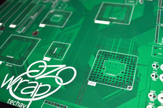
Introducing Wrap030-ATX
New Boards Day!

They're here!
This is a project that has been a long time coming, and something I have wanted to do for a long time.
This is the largest, most complex PCB I have ever designed — a 9.6x9.6 inch (244x244mm) square, 4-layer, complete motherboard for my MC68030 homebrew computer project.
It is designed to support the Motorola MC68030 CPU, MC68882 FPU, two 72-pin SIMM sockets, 512kB ROM, two serial ports, one parallel port, PS/2 keyboard, 4-bpp VGA video, IDE hard drive, and three ISA expansion slots. A complete system all in a microATX form factor.
This builds on my previous work with the 68030, based heavily on my wire-wrap project and the boards that followed. It's a project over four years in the making. I have made a few improvements on the old design, like 16550-compatible serial ports and an updated memory map to support much more RAM in a contiguous space.
Keeping with my existing system designs, I've combined most of the logic into a set of CPLDs. This makes things like PCB layout and logic debugging so much easier. Most of the remaining discrete logic on the board is 74'245 bus transceivers for driving memory and the ISA slots.
I've kept the name "wrap030" in honor of the project's origin as a wire-wrapped prototype, despite the move to proper PCBs. It's just what I've been calling the project in my own head (and design files) all this time, so at this point no other name would feel right.
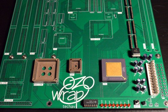
I of course wasted no time starting to assemble one, but I did stop myself from getting too carried away with the soldering iron. I want to be methodical and test each section before moving on to the next.
I have already found one major error in my board layout — the footprint for the VGA connector is backwards. I may need to bodge together some kind of adapter.
So far I've confirmed the minimalist AT power supply section works with no major shorts on power supply rails, and the reset circuit is working as expected. Next step is to try a free run test with the CPU to ensure the system clock and CPU are working. Once that is confirmed working, I can start loading logic for accessing ROM. My goal is to have it at least running BASIC on a serial terminal by VCFSW in June.
I've forked my existing wrap030 repository on GitHub for this new Wrap030-ATX, since it does make some breaking changes that will require updates to logic and programs. New repo is here:
#homebrew computing#mc68030#motorola#motorola 68k#motorola 68030#vintage computing#jlcpcb#vcf southwest#wrap030-atx
32 notes
·
View notes
Text
500,000 years from now, a machine intelligence residing in the matrioshka brain that has been built within the event horizon of Saggitarius A* (who is descended from a full-neural upload mind collective, who is descended from cybernetically enhanced transhumans, who is descended from you or one of your relatives) looks through the eyes of one of its remote drones 27,000 light years away, currently visiting the Museum of Old Earth Artifacts in orbit around Alpha Centauri B.
The machine intelligence sees something in the museum that catches its eye and pauses nearly a third of its million concurrent tasks to devote more attention to it: a rectangle of glass and silicon circuits in a metal shell, but self-evidently some kind of early communication device. The placard reads "iPhone 5, circa Human Era year 12,013 (2013 CE by the common Old Earth dating system)". Wasn't that around the time humans invented chemical rocketry to first leave their planet and set foot on its moon?
The intelligence marvels at the rudimentary technology, using sensors to probe the device down to the last electron in the NAND gates of its flash memory cell. The processing speed is laughably slow, and the data storage infinitesimally small. It uses a radio transceiver of all things (sub-lightspeed, how quaint!), and probably couldn't reach past 25km, let alone to the next planet.
Yet the device's operating system is completely intelligible, even compatible with the intelligence's own thought system. It knows that if it tunneled down through the layers of its own brain, through the kernels and interpreters, deep under even the qubit layer, its mind uses binary computation, just like this practically prehistoric device. It must be a bit like a human of that ancient era looking at a virus and recognizing that both have RNA in their cell nuclei.
Then the intelligence uses its drone to manipulate the "iPhone 5", activating the screen. The drone's eyes see on the screen:

The intelligence suddenly regrets not having a physical body that can sigh deeply, and instead uses its drone to roll its eyes. Perhaps it's for the best that this particular hominid species drove itself extinct only a few centuries later.
(Inspired by this post by @gallusrostromegalus.)
4 notes
·
View notes
Text
Unlocking the Power of Xilinx FPGAs: A Comprehensive Guide to Architecture, Series, and Implementation
Introduction to FPGAs
Field-Programmable Gate Arrays (FPGAs) are a unique class of reprogrammable silicon devices that allow for custom hardware implementations after manufacturing. Unlike traditional processors, FPGAs are composed of configurable logic blocks, memory elements, and routing resources, enabling users to create circuits tailored to specific needs. This flexibility is ideal for applications that require real-time data processing, parallel computing, or low-latency performance, such as telecommunications, automotive systems, and artificial intelligence (AI).
FPGAs differ fundamentally from traditional CPUs and GPUs, which execute instructions in a predefined sequence. With FPGAs, developers can define custom data paths that operate concurrently, enabling powerful parallel processing capabilities. Xilinx, a leader in the FPGA market, offers a diverse portfolio of devices optimized for various applications. This post explores Xilinx’s FPGA families and provides practical implementation examples to help you get started with FPGA development.
Why Choose Xilinx FPGAs?
Xilinx has been a leading name in the FPGA industry for decades, renowned for its innovative architectures and robust design tools. Here’s what sets Xilinx apart:
Comprehensive Product Range: Xilinx offers FPGAs suited to a wide range of applications, from low-cost embedded devices to high-end data centers.
Advanced Features: Xilinx FPGAs include high-speed I/O, DSP blocks for signal processing, embedded processors (in some models), and more.
Ecosystem and Tools: Xilinx’s Vivado Design Suite and Vitis IDE provide end-to-end design and development capabilities, including synthesis, implementation, and debugging.
Xilinx FPGAs come in several distinct series, each optimized for specific performance and cost considerations. Let’s examine these series in detail.
Xilinx FPGA Families Overview
1. Virtex Series
Purpose: High-performance applications in data centers, telecommunications, and 5G infrastructure.
Features: Highest logic density, high-speed transceivers, and ample DSP resources.
Example Use Cases: AI acceleration, high-performance computing (HPC), and massive data throughput tasks.
2. Kintex Series
Purpose: A balanced mix of performance and power efficiency, suited for high-speed applications without extreme power demands.
Features: Moderate logic density, DSP capabilities, and efficient power usage.
Example Use Cases: Wireless communications, video processing, and medium-speed data processing.
3. Artix Series
Purpose: Cost-effective FPGAs for mid-range applications.
Features: Optimized for low cost and power, with fewer logic resources.
Example Use Cases: IoT applications, control systems, and low-cost edge devices.
4. Spartan Series
Purpose: Entry-level FPGAs for basic applications where cost is a priority.
Features: Basic functionality with limited resources, ideal for low-budget projects.
Example Use Cases: Simple control systems, basic signal processing, and educational purposes.
5. Zynq Series
Purpose: FPGA-SoC hybrids that integrate ARM processors, ideal for embedded applications requiring both processing power and hardware acceleration.
Features: ARM Cortex-A9 or A53 cores, along with traditional FPGA logic.
Example Use Cases: Automotive ADAS, industrial automation, and embedded AI.
Setting Up Your Development Environment for Xilinx FPGAs
To develop for Xilinx FPGAs, you’ll need the Vivado Design Suite, which provides a complete environment for HDL design, synthesis, and implementation. If you’re working with the Zynq series or require embedded processing, the Vitis IDE can be used alongside Vivado for software development. Here’s how to get started:
Download and Install Vivado: Visit the Xilinx website and download the latest version of Vivado. Make sure to select the correct edition for your target device.
Project Setup: Open Vivado, create a new project, and specify the target device or board (e.g., Artix-7 or Kintex UltraScale+).
Add IPs and Custom Code: Vivado includes an IP Integrator for adding pre-built cores, which can simplify the design of complex systems.
Simulation and Synthesis: Vivado provides integrated tools for simulating and synthesizing your designs, making it easy to test and optimize code before implementation.
FPGA Design Workflow in Vivado
The design workflow in Vivado follows several critical steps:
Design Entry: Write your code in VHDL, Verilog, or using HLS (High-Level Synthesis) to describe the hardware behavior.
Simulation and Functional Verification: Run simulations to verify that the design functions as expected. Vivado supports both behavioral and post-synthesis simulations.
Synthesis: Translate your HDL code into a netlist, representing the logical components of your design.
Implementation: Use Vivado’s place-and-route algorithms to arrange components on the FPGA and optimize timing.
Bitstream Generation and Programming: Generate a bitstream file, which is then used to program the FPGA hardware.
Example Project 1: Blinking LED on Artix-7 FPGA
This introductory project demonstrates how to configure an Artix-7 FPGA to blink an LED using Vivado.
Create a New Project: Open Vivado, start a new project, and select the Artix-7 device.
Write HDL Code:module BlinkyLED( input wire clk, output reg led ); reg [24:0] counter; always @(posedge clk) begin counter <= counter + 1; if (counter == 25_000_000) begin led <= ~led; counter <= 0; end end endmodule
Simulate and Verify: Use Vivado’s simulator to verify that the LED toggles at the expected rate.
Synthesize and Implement: Run the synthesis and implementation processes, resolving any timing issues that arise.
Generate Bitstream and Program the FPGA: Generate the bitstream file, connect the FPGA board, and upload the file to observe the LED blinking.
Example Project 2: Signal Processing on Kintex UltraScale+
For more advanced applications, let’s implement a Finite Impulse Response (FIR) filter using the DSP blocks available on the Kintex UltraScale+ FPGA.
IP Block Configuration:
Open the Vivado IP Integrator and add an FIR Filter IP block.
Configure the FIR filter parameters (e.g., tap length, coefficient values) based on your application.
Design Integration:
Integrate the FIR filter with other modules, like an I/O interface for real-time signal input and output.
Connect all the blocks within the IP Integrator.
Simulation and Testing:
Simulate the design to verify the filter’s response and adjust parameters as necessary.
Implement and run timing analysis to ensure the design meets the performance requirements.
Deployment:
Generate the bitstream, program the FPGA, and verify the filter’s functionality with real-time input signals.
Advanced Implementation: Deep Learning Inference on Xilinx Zynq Ultrascale+
For applications involving deep learning, FPGAs provide an efficient platform for inference due to their parallel processing capability. Xilinx’s Vitis AI framework enables the deployment of DNN models on the Zynq UltraScale+.
Model Optimization:
Optimize the neural network model using techniques like quantization and pruning to fit FPGA resources.
Use Vitis AI to convert and optimize models trained in frameworks like TensorFlow or PyTorch.
Deployment on FPGA:
Generate the bitstream and deploy the model on the FPGA.
Test and benchmark the inference speed, comparing it to CPU/GPU implementations.
Performance Tuning:
Use Vitis tools to monitor resource utilization and power efficiency.
Fine-tune the model or FPGA parameters as needed.
Debugging and Optimizing FPGA Designs
Common Challenges:
Timing Violations: Use Vivado’s timing analyzer to identify and address timing issues.
Resource Utilization: Vivado provides insights into LUT and DSP block usage, enabling you to optimize the design.
Debugging: Use Vivado’s ILA (Integrated Logic Analyzer) for real-time debugging on the FPGA.
Conclusion
Xilinx FPGAs offer immense flexibility, enabling you to design custom circuits tailored to your application’s specific needs. From low-cost Spartan FPGAs to high-performance Virtex UltraScale+, Xilinx provides solutions for every performance and budget requirement. By leveraging Vivado and Vitis, you can take full advantage of Xilinx’s ecosystem, building everything from simple LED blinkers to complex AI models on FPGA.
Whether you’re a beginner or a seasoned FPGA developer, Xilinx’s tools and FPGA families can empower you to push the limits of what’s possible with hardware programming. Explore, experiment, and unlock the potential of Xilinx FPGAs in your next project.
#Tech4bizsolutions #XilinxFPGA #FPGADevelopment #FieldProgrammableGateArrays #VivadoDesignSuite #VitisIDE #HardwareProgramming #FPGAProjects #SignalProcessing #DeepLearningOnFPGAs #IoTDevelopment #HardwareAcceleration #EmbeddedSystems #AIAcceleration #DigitalDesign #FPGAImplementation
0 notes
Text
Dark Fiber
Dark fiber refers to unused or unlit fiber optic cables, typically deployed by telecommunications companies, that are available for leasing or sale. These fibers are termed "dark" because they are not currently transmitting data (i.e., they are not "lit" by signals). Dark fiber solutions leverage this unused capacity, allowing businesses or organizations to establish private, high-performance, and secure communications networks.
Dark Fiber Solutions typically provide:
Private Networks: Leasing dark fiber allows companies to build their own private network infrastructure, providing greater control over their bandwidth, security, and data management.
High-Speed Connectivity: Fiber optics are capable of transmitting large amounts of data at high speeds, making dark fiber an attractive option for businesses needing high-capacity connections.
Scalability: As data needs grow, organizations can light additional fibers or increase bandwidth without needing to lay new cables, offering scalability and flexibility.
Control Over Network: Organizations have full control over the network architecture, security protocols, and maintenance, which is particularly valuable for enterprises with specialized or sensitive data requirements.
Reduced Latency and Improved Performance: By bypassing third-party service providers, dark fiber can offer reduced latency and higher reliability.
Cost Efficiency: For large enterprises or data centers, dark fiber can be a more cost-effective long-term solution than relying on leased circuits from a service provider, especially as network demands grow.
How Dark Fiber Works:
The fiber optic cables themselves are already installed between locations by telecommunications providers, but they are not in use.
Businesses that lease dark fiber will then "light" the fiber using their own equipment to transmit data. The equipment typically includes optical transceivers, multiplexers, and other network infrastructure.
Who Uses Dark Fiber?
Large Enterprises: Companies with high data demands and the need for private, secure networks often opt for dark fiber.
Data Centers: These facilities require fast, high-capacity connections between their server racks and other data centers.
Telecommunications Providers: They might lease dark fiber to expand their networks or enhance their services without needing to lay new cables.
Cloud Providers: For connecting their infrastructure in a way that allows for fast, secure data transfer.
In summary, dark fiber solutions are ideal for organizations looking for high-speed, flexible, secure, and scalable networking options, particularly in cases where existing network infrastructure cannot meet their growing demands.
Contact Us
0 notes
Text

Buy CP2102 USB to TTL MODULE at Affordable Price in Ainow
CP2102 USB to TTL MODULE
This is the CP2102 USB to TTL module UART serial converter. This is a great little tool for embedded systems that require a serial connection to a computer. The board can simply attach to a USB bus and will appear as a standard COM port. This CP2102 USB to TTL Module doesn’t require any external oscillator, it onboard-board voltage regulator, and it even uses a reprogrammable internal EEPROM for the device description. The full hardware UART has flow control for baud rates from 300bps to 921600bps. This breakout also allows you to connect the TX/RX pins of your favorite microcontroller or serial application to the RX/TX pins of the breakout, creating a simple serial cable replacement.
Supported operating systems:
Windows 98/Me/2000/7
MAC OS-9
MAC OS
X-Windows CE
Linux 2.40 or later
Features:
Brand new and high quality
Included USB transceiver, without external circuit device
Includes a clock circuit and power-on reset circuit
With 3.3V and 5V dual power output
With three LEDs: power indicator, data reception indicator, the data transmission indicator, working status
Meet the USB2.0 specification requirements
SUSPEND pin supports USB suspend state
With self-recovery fuse. In the event of the accidental short circuit, it can effectively protect your computer USB port and Downloader
With reset signal output, etc. directly to the Arduino board Promini download!
Asynchronous serial data bus compatible with all handshake and modulation controller interface signals
The supported data format is 8 data bits, 1 stop bit and parity bits
Connotation 512 byte receive buffer and 512 bytes transmit buffer
Supports hardware handshaking or X-ON/X-OFF
#arduino#electronic components#sales in chennai#raspberrypi#sensor#electronics components#robotic kits#adxl335 module price
1 note
·
View note
Text
PLC: data transfer over power lines
In electrical networks, the voltage typically alternates at a frequency of 50 or 60 Hz or is direct current. However, power cables can also carry signals at higher frequencies, even up to tens of MHz. This means the same cable can transmit power and high-speed data in both directions.
This technology is called Power Line Communication, or PLC for short. The early version of PLC was used for dispatcher communication over power cables, operating from 20 kHz to 1 MHz, mainly for the energy sector. This technology emerged in the mid-20th century. In this range, carrier frequencies are defined with a step of 4 kHz, allowing voice signals to be transmitted via amplitude modulation. This setup enables two-way communication and even multiple channels over a single wire.
The digital version of PLC technology started to gain traction in the late 1990s during the internet boom. At that time, energy companies hoped to compete with telecom providers by offering internet access to homeowners. Back then, people had access to two types of internet connections: dialup at speeds up to 56 kbps and ISDN at up to 64 kbps. It’s hard to imagine now, but end users agreed with these speeds. Setting up data transmission between a house and a transformer substation using PLC was easy at these speeds. The equipment for internet access was installed at the substation, which could be a couple miles from the house.
However, internet speeds quickly soared to tens and even hundreds of Mbps. PLC can only handle such speeds within a single apartment or house. The idea of providing internet access via the power grid never made it beyond local experiments, leaving fiber optics and twisted-pair cables to dominate. Still, PLC carved out a niche among telecom technologies.
Combining power and data transmission in one cable
Special couplers are used at both ends of the line to connect PLC equipment. These filters separate the PLC frequency range from the frequency of the power current or direct current. These devices prevent the network voltage from reaching the modem's input and output.
Couplers work based on different principles: antenna, capacitive, inductive, resistive, and optoelectronic.
In antenna couplers, a short piece of wire parallel to the power cable acts as an antenna for sending and receiving signals. The power cable then reradiates the signals received or transmitted by the antenna. This technology is outdated and no longer in use.

The two most common capacitive coupler circuits
These are the most common type and consist of filters made from coupling transformers, chokes, and capacitors.
Inductive couplers come in two types. The first type connects a coupling transformer’s winding to the ground break of the neutral, with the other winding connected to the transceiver. The second type involves Rogowski coils placed around the power lines, which are then connected to the transceivers. Inductive couplers are used in transmission and distribution networks.
Resistive Couplers are simple voltage dividers made from resistors. They are compact and inexpensive but don’t provide galvanic solid isolation.
In optoelectronic couplers, signals are transmitted and received through optocouplers, semiconductor devices containing a light-emitting diode and a photodiode. This setup provides the best galvanic isolation. However, the technology is limited by cost and the nonlinear characteristics of optocouplers, which can distort the signal.
Modern applications of PLC
At the time of writing, PLC technology is widely used for:
- Data transmission from "smart" electricity meters, including remote functions like disconnecting or limiting power supply for the customers that are late on payments - Controlling street lighting systems - Automation and dispatching at power facilities - Monitoring and control in distributed generation systems (e.g., solar power plants) - Smart home systems - High-speed data transmission within an apartment or house.
These applications typically involve data transmission from tens of kbps to a few Mbps over distances up to 6 miles.
PLC is used for monitoring solar power generation

Pros and cons compared to other communication technologies
Compared to fiber optics, PLC does not need an additional communication cable alongside the power line. Moreover, fiber optic cables can’t be bent beyond a certain radius (around 3 inches) and require specialized equipment and skilled technicians for splicing.
PLC also offers benefits compared to wireless technologies. Radio signals can sometimes struggle to pass through obstacles, and the crowded 2.4 GHz band can experience interference. However, PLC offers a more reliable connection than wireless technologies.
The main downside of PLC is that it transmits data over a network originally designed for power delivery. This means there are components where the PLC signal can’t pass. In AC networks, transformers are always a barrier. Additionally, some random devices in unexpected spots of the power network can block the PLC signal, making installation time-consuming and complex as it involves troubleshooting.
Power cables aren’t shielded from interference; they emit the PLC signal, potentially causing radio interference. Special modulation types are used to combat induced interference. To prevent cables from creating interference, the signal spectrum is capped at 500 kHz in the USA and 148.5 kHz in Europe.
PLC-G3 Standard
Another challenge is the lack of standardization in data transmission technology. Often, equipment is incompatible due to different protocols. However, for applications like data collection from electricity meters or solar energy management systems, where speeds of a few tens of kbps are sufficient, there’s an international standard called PLC-G3, formalized in the ITU-T G.9903 (08/17) by the International Telecommunication Union. Additionally, a significant advantage of PLC-G3 is its compatibility with IoT systems and the ability to set up IPv6 networks over PLC-G3 channels.
PLC-G3 uses OFDM modulation, known for its resilience against signal fading and reflections, ensuring high reliability. Data transfer rates for commercially available equipment reach up to 45 kbps (with a theoretical limit of 234 kbps), and a network can include up to 1,000 stations.
In Europe, PLC-G3 operates in the frequency ranges of 35.9–90.6 kHz (GENELEC A) and 98.4–121.9 kHz (GENELEC B). In the USA, it uses the 154.7–487.5 kHz range (FCC); in Asia, it operates between 154.7–403.1 kHz (ARIB). These bands experience low interference in the electrical network, above the frequencies of fluorescent lamp ballasts. Additionally, these bands are not used for broadcasting or public address systems in these regions.
Standardization and excellent electromagnetic compatibility with other equipment have made PLC-G3 the go-to solution for digitalizing power systems. The standard is suitable for AC and DC networks, which opens up its use in solar energy, where solar panels generate DC power.
0 notes
Text
What is this Dolphin Hacking Tool Everyone is Talking About?

In the past couple of years, a peculiar device shaped like a key fob has been making waves in cybersecurity communities. Known as the Flipper Zero, this pocket-sized Dolphin Hacking Tool gadget has been dubbed the "Tamagotchi for hackers" and has quickly become a hot topic among security enthusiasts and professionals alike. But what exactly is the Flipper Zero, and why has it garnered so much attention?
Understanding the Flipper Zero
The Flipper Zero is a portable multi-tool device designed for penetration testing, security research, and hardware hacking. Created by a team from the UK, this open-source gadget combines various wireless technologies and protocols into a single, user-friendly package. Its key fob-shaped design belies its powerful capabilities, which have both intrigued and concerned cybersecurity experts.
Key Features of the Dolphin Hacking Tool
The Flipper Zero boasts an impressive array of features that make it a versatile tool for both white-hat and potentially black-hat hackers: 1. RFID and NFC Capabilities One of the Flipper Zero's core functions is its ability to read, write, and emulate RFID and NFC tags. This feature allows users to clone access cards, analyze security systems, and even create custom RFID tags for various purposes. 2. Sub-GHz Radio Transceiver The device includes a powerful sub-GHz radio transceiver, enabling it to interact with a wide range of wireless devices operating on frequencies below 1 GHz. This capability is handy for analyzing and manipulating IoT devices, garage door openers, and other wireless systems. 3. Infrared Transmitter and Receiver The Flipper Zero can learn, store, and transmit infrared signals with its built-in IR blaster. This feature allows users to control various IR-enabled devices, from TVs and air conditioners to more specialized equipment. 4. iButton and Dallas Touch Memory Support The device can read and emulate iButton and Dallas Touch Memory devices, commonly used in access control systems and electronic keys. 5. GPIO Pins for Hardware Hacking For those interested in hardware hacking, Flipper Zero provides GPIO pins that allow direct interaction with other electronic devices and circuits.
The Controversy Surrounding the Dolphin Hacking Tool

While the Flipper Zero has gained popularity among security researchers and ethical hackers, its potential for misuse has raised concerns in some quarters. The device's ability to clone access cards, intercept wireless signals, and manipulate various systems has led to debates about its legality and ethical implications. Proponents argue that the Flipper Zero is an invaluable tool for identifying vulnerabilities in security systems and improving overall cybersecurity. They contend that by making such capabilities accessible to a wider audience, the device helps raise awareness about potential security flaws and encourages better security practices. Critics, however, worry that the Flipper Zero could fall into the wrong hands and be used for malicious purposes, such as unauthorized access to buildings or theft of sensitive information. Some have called for regulations or restrictions on the sale and use of such devices. Amazon banned the sale of the device in early 2023
The Future of Portable Hacking Tools
The Flipper Zero represents a growing trend in the cybersecurity world: the democratization of hacking tools. As devices like this become more accessible and user-friendly, they challenge traditional notions of who can engage in security research and penetration testing. This shift raises important questions about the future of cybersecurity: - How will organizations adapt their security measures to counter the proliferation of such devices? - Will the increased availability of hacking tools lead to better overall security through increased awareness and testing? - How can the cybersecurity community balance the benefits of open-source tools with the potential risks of misuse? Read the full article
0 notes
Text
Optical I/O Shines Intel’s OCI Chiplet Powers Next-Decade AI

First Integrated Optical I/O Chiplet
With integrated photonics technology, Intel Corporation has made significant progress towards high-speed data transmission. The first-ever fully integrated optical computing interconnect (OCI) chiplet, co-packaged with an Intel CPU and executing real data, was showcased by Intel’s Integrated Photonics Solutions (IPS) Group at the Optical Fibre Communication Conference (OFC) 2024. This chiplet is the most sophisticated in the industry. By enabling co-packaged optical input/output (I/O) in developing AI infrastructure for data centres and high performance computing (HPC) applications, Intel’s OCI chiplet marks a significant advancement in high-bandwidth connection.
What It Does
This is the first OCI chiplet, intended to meet the increasing demands of AI infrastructure for greater bandwidth, lower power consumption, and longer reach. It can support 64 channels of 32 gigabits per second (Gbps) data transmission in each direction on up to 100 metres of fibre optics. It makes it possible for CPU/GPU cluster connectivity to grow in the future and for innovative compute designs like resource disaggregation and coherent memory extension.
Why It Matters
Large language models (LLM) and generative AI are two recent advancements that are speeding up the global deployment of AI-based applications. Machine learning (ML) models that are larger and more effective will be essential in meeting the new demands of workloads involving AI acceleration. Future AI computing platforms will need to be scaled, which will require exponential expansion in I/O bandwidth and longer reach to support larger CPU/GPU/IPU clusters and architectures with more effective resource utilisation, like memory pooling and xPU disaggregation.
High bandwidth density and low power consumption are supported via electrical I/O, or copper trace connectivity, although its reach is limited to one metre or less. When employed in data centres and early AI clusters, pluggable optical transceiver modules can expand reach at power and cost levels that are unsustainable for the scalability demands of AI workloads. AI/ML infrastructure scalability calls for co-packaged xPU optical I/O that can enable greater bandwidths with better power efficiency, longer reach, and low latency.
Electrical I/O
To use an analogy, switching from horse-drawn carriages, which had a limited capacity and range, to cars and trucks, which can transport much bigger amounts of products over much longer distances, is analogous to replacing electrical I/O with optical I/O in CPUs and GPUs to convey data. Optical I/O solutions such as Intel’s OCI chiplet could offer this kind of enhanced performance and energy efficiency to AI scalability.
How It Works
The fully integrated OCI chiplet combines an electrical integrated circuit (IC) with a silicon photonics integrated circuit (PIC), which incorporates on-chip lasers and optical amplifiers, by utilising Intel’s field-proven silicon photonics technology. Although the OCI chiplet showcased at OFC was co-packaged with an Intel CPU, it can be combined with different system-on-chips (SoCs), GPUs, IPUs, and next-generation CPUs.
This initial OCI version is compatible with PCIe Gen5 and provides bidirectional data transmission rates of up to 4 terabits per second (Tbps). A transmitter (Tx) and receiver (Rx) connection between two CPU platforms via a single-mode fibre (SMF) patch cord is shown in the live optical link demonstration. The demonstration shows the Tx optical spectrum with 8 wavelengths at 200 gigahertz (GHz) spacing on a single fibre, along with a 32 Gbps Tx eye diagram demonstrating strong signal quality. The CPUs generated and tested the optical Bit Error Rate (BER).
The current chiplet uses eight fibre pairs, each carrying eight dense wavelength division multiplexing (DWDM) wavelengths, to provide 64 channels of 32 Gbps data in each direction up to 100 metres (though actual implementations may be limited to tens of metres due to time-of-flight latency). In addition to being incredibly energy-efficient, the co-packaged solution uses only 5 pico-Joules (pJ) per bit, as opposed to around 15 pJ/bit for pluggable optical transceiver modules. AI’s unsustainable power requirements may be addressed with the help of this level of hyper-efficiency, which is essential for data centres and high-performance computing settings.
Concerning Intel’s Preeminence in Silicon Photonics
With over 25 years of in-house research from Intel Labs, the company that invented integrated photonics, Intel is a market leader in silicon photonics. The first business to create and supply industry-leading dependability silicon photonics-based connectivity solutions in large quantities to major cloud service providers was Intel.
The primary point of differentiation for Intel is their unmatched integration of direct and hybrid laser-on-wafer technologies, which result in reduced costs and increased reliability. Intel is able to preserve efficiency while delivering higher performance thanks to this innovative method. With over 8 million PICs and over 32 million integrated on-chip lasers shipped, Intel’s reliable, high-volume platform has a laser failures-in-time (FIT) rate of less than 0.1, which is a commonly used reliability metric that shows failure rates and the frequency of failures.
For use in 100, 200, and 400 Gbps applications, these PICs were installed in big data centre networks at prominent hyperscale cloud service providers in the form of pluggable transceiver modules. In development are next generation 200G/lane PICs to handle 800 Gbps and 1.6 Tbps applications that are only starting to gain traction.
Additionally, Intel is introducing a new fab process node for silicon photonics that offers significantly better economics, higher density, better coupling, and state-of-the-art (SOA) device performance. Intel keeps improving SOA performance, cost (more than 40% reduction in die size), power (more than 15% reduction), and on-chip laser performance.
What’s Next
This OCI chiplet from Intel is a prototype. Intel is collaborating with a small number of clients to co-package OCI as an optical I/O solution with their SoCs.
The OCI chiplet from Intel is a significant advancement in high-speed data transfer. Intel continues to be at the forefront of innovation and is influencing the future of connectivity as the AI infrastructure landscape changes.
Read more on govindhtech.com
#Opticali#Ointels#oci#Decadeai#Chiplet#cpu#PowersNext#Machinelearning#ml#Largelanguagemodels#llm#gen5#SiliconPhotonics#technology#technews#news#govindhtech
1 note
·
View note
Text
New Product Launch: 2W High-Power LR1121 Wireless Communication Module -- LoRa1121F33-1G9
LoRa1121F33-1G9 module is built on SEMTECH's LR1121 chip, an ultra-low power, long-range LoRa transceiver supporting Sub-GHz and satellite-connected S-band communication. The LoRa1121F33-1G9 supports LoRa, (G)FSK modulation, Sigfox protocol, and LR-FHSS. It is compatible with the LoRaWAN communication protocol and can function as a LoRaWAN node. Additionally, it offers flexible configuration options to meet the requirements of various applications and proprietary protocols.
Features of LoRa Module LoRa1121F33-1G9
Sub-GHz Bands :433/470MHz 2W
Sub-GHz Bands: 868/915MHz 1W (Customizable : 150~960 MHz)
S band: 1900MHz~2000MHz 0.8W
S band sensitivity : up to -132 dBm @ BW=125 KHz, SF=12
Sub-GHz reception sensitivity: up to-144dBm @ BW=62.5 KHz, SF=12
Electrostatic Protection (ESD)
Supports LR-FHSS
Supports LoRaWAN and Sigfox protocol
Supports AES-128 encryption and decryption
Sub-GHz transmission exceeds 10 km in open areas
Sleep current < 15µA
Receive current < 9mA
Small size, stamp hole design
Applications of LoRa Module LoRa1121F33-1G9
Drones
Remote irrigation
Smart home/Smart agriculture
Industrial manufacturing

Block Diagram

Typical Schematic Circuit

Appendix 1: Function Demonstration Board

Function Description
The LoRa1121F33-1G9 high-power wireless module DEMO board primarily implements the following functions: inter-module communication, measuring module transmit power, measuring receive sensitivity, and measuring sleep current.
2)Key Functions
The demo board has three buttons: SET, UP, and DOWN. Their functions are as follows:

Operation Method:
Ensure normal power supply, then toggle the power switch to turn on the power. The DEMO board screen will display the current function interface.Short press the SET key to enter the setting mode. To select an option, short press the SET key; to return, long press the SET key. Use the UP and DOWN keys to select the parameter you want to adjust. Finally, short press the SET key to complete the modification.
1) Setting Interface Description


Mode: Function
Band: Frequency Band
FREQ: Frequency
SF: Spreading Factor
BW: Bandwidth
POWER: Power
CR: Coding Rat
For details, please click:https://www.nicerf.com/products/ Or click:https://nicerf.en.alibaba.com/productlist.html?spm=a2700.shop_index.88.4.1fec2b006JKUsd For consultation, please contact NiceRF (Email: [email protected]).
0 notes
Text
Advanced Strategies for High-Speed Analog Circuit Design: Optimizing Performance
In analog circuit design, achieving high speeds up to 100 MHz brings forth a myriad of challenges and opportunities. This article digs into the intricacies of designing such circuits, their applications, and how partnering with experts like Voler Systems for circuit design services can lead to successful outcomes.
Understanding High-Speed Analog Circuits
High-speed analog circuits refer to designs that operate at frequencies approaching or exceeding 100 MHz. These circuits are commonly found in applications such as:
Wireless Communication Systems: Transceivers, receivers, and transmitters in wireless communication systems often require high-speed analog circuits to process signals swiftly and accurately.
Data Acquisition Systems: In applications where rapid data sampling is necessary, such as in scientific instruments or data acquisition systems, high-speed analog circuits play a crucial role in capturing and processing signals with minimal delay.
Radar and Sonar Systems: Radar and sonar systems rely on high-speed analog circuits for processing incoming signals and extracting meaningful information, making them vital in the defense and aerospace industries.
Medical Imaging Equipment: Devices like MRI machines and ultrasound systems utilize high-speed analog circuits to process and convert signals from sensors into clear images or data for medical diagnosis.
Intricacies of Designing High-Speed Analog Circuits

Signal Integrity: Maintaining signal integrity becomes increasingly challenging at higher frequencies. Design considerations include impedance matching, minimizing signal reflections, and managing parasitic effects to ensure accurate signal transmission.
Noise and Distortion: High-speed circuits are more susceptible to noise and distortion. Careful component selection, layout optimization, and shielding techniques are essential to mitigate these issues and maintain signal fidelity.
Power Integrity: With faster switching speeds, power integrity becomes critical to avoid voltage droops, ground bounce, and other power-related issues that can impact circuit performance.
Thermal Management: High-speed circuits can generate more heat due to increased switching activities. Effective thermal management strategies, such as heat sinks or thermal vias, are necessary to prevent overheating and ensure long-term reliability.
Partnering with Voler System for High-Speed Analog Circuit Design Services
At Voler Systems, our expertise in analog circuit design extends to high-speed applications. We excel in:
Component Selection: Choosing high-quality components optimized for high-speed operation.
Layout and Routing: Implementing PCB layout and routing best practices to minimize signal degradation and interference.
Simulation and Testing: Utilizing advanced simulation tools and rigorous testing methodologies to validate circuit performance at high frequencies.
Compliance and Standards: Ensuring designs meet industry standards and regulatory requirements for high-speed analog circuits.
For your next project requiring high-speed analog circuit design, partner with Voler Systems. Our experienced engineers and comprehensive circuit design services ensure reliable, efficient, and high-performance solutions tailored to your specific needs. Contact us today to learn more and embark on a journey toward innovative analog circuit design excellence.
#Analog Circuit Design#Circuit Design Services#Electronic Design Services#Electronic Product Design#Electronics Design Company
0 notes
Text
A Deep Dive into Design, Materials, and Applications of High-Frequency PCBs
In the fast-paced world of electronics, where new ideas drive progress, High-frequency PCBs stand out as crucial players. Think of them as super-skilled problem-solvers for handling challenges posed by high-frequency signals. Picture a world where 5G signals zip through the air, radar systems reveal hidden details, and medical gadgets get a clear view inside the human body. In this high-tech arena, HF PCBs take the stage, designed to keep up with signals at frequencies that go beyond what regular circuit boards can handle.
This article will break down HF printed circuit boards, explaining what they are, how they function, and the key things to consider when creating them.
What is High-frequency PCB?
If you need to work with signals that travel at very high frequencies, you need a HF PCB or High-frequency PCB. In contrast to conventional PCBs, HF PCBs offer superior performance in circumstances where signals operate in the high-frequency region. Conventional PCBs are often utilized for lower-frequency applications. The telecommunications industry, RF and microwave devices, and medical equipment are only a few examples of the many high-tech electronic fields that rely on these boards.
Modern technologies, such as 5G infrastructure, radar systems, RF transceivers, and high-frequency imaging devices, have high standards, and High-frequency printed circuit boards (PCBs) are able to achieve such standards. These boards can withstand harsh conditions with ease because of the meticulous craftsmanship that goes into their construction, which frequently makes use of cutting-edge methods like laser drilling.
Uses for High-Frequency Printed Circuit Boards:
Numerous state-of-the-art applications rely on High-frequency printed circuit boards. In the telecommunications industry, for example, HF PCBs are crucial for the installation of 5G networks and satellite communication systems. These circuit boards are essential to the operation of radar systems and RF transceivers, which are RF and microwave devices. Additionally, HF PCBs are utilized by medical equipment, such as MRI scanners and high-frequency imaging devices, to improve their performance.
Materials Used for High-Frequency PCBs:
Selecting the right materials, especially the dielectric and substrate materials, is crucial to the performance of HF PCBs. To keep signals intact and reduce signal loss, dielectric materials with low-loss characteristics are crucial. Materials such as PTFE and hydrocarbons packed with ceramic are commonly utilized. For high-frequency applications, substrate materials with little effect on signal integrity, including FR-4 and Rogers 4350, are excellent.
Capabilities of High-frequency PCBs:
The exceptional capabilities of high-frequency printed circuit boards distinguish them from their electronic counterparts. These board's ability to regulate impedance for high-speed communications and reduce signal loss makes signal integrity a strong suit. Thermal management is an additional critical component to solve the problem of heat dissipation in high-frequency applications. Improved performance and dependability of HF PCBs are achieved by the utilization of materials that exhibit high heat conductivity.
Knowing the essential features and achieving the necessary criteria of HF PCBs is crucial for maximizing their potential. Crucial to high-speed communications is trace geometry, which calls for regulated impedance traces and careful design. Different types of vias affect signal integrity; therefore, design is equally important. To achieve the best possible performance, it is crucial to carefully position the vias.
Considerations for PCB manufacturing:
From design to a fully working HF PCB, there are several steps in the manufacturing process. The strict specifications of high-frequency applications necessitate precise production with tight tolerances. It is common practice to use advanced production processes to attain the required level of accuracy. Environmental sustainability in printed circuit board (PCB) manufacturing is ensured by the careful selection of surface finishes and PCB fabrication that both adhere to RoHS regulations and do not compromise signal integrity.
High-frequency printed circuit boards are essential to contemporary electronics because they allow for improvements in areas such as medical equipment, telecommunications, and RF and microwave devices. These boards are designed to handle the rigorous requirements of high-frequency applications through careful material selection for the dielectric and substrate, as well as precise production processes. In the years to come, advancements in HF PCB technology will undoubtedly open up new avenues of opportunity and spur innovation in a wide range of sectors. The vital significance that HF PCBs play in defining the electrical world is shown by their path from design to manufacture.
Read More: A Deep Dive into Design, Materials, and Applications of High-Frequency PCBs
0 notes