#pcb soldering manufacturers
Explore tagged Tumblr posts
Visit Tumblr Blog
Explore Tumblr blogs with no restrictions, modern design and the best experience.
Last Seen Tumblr Blogs


Fun Fact
Women make up for the other 50% of Tumblr’s audience.
Text
SELECTIVE SOLDER 🔬🔥🔧
Selectively soldering components to printed circuit board (PCBs), while avoiding heat-sensitive parts - ensuring that only the desired areas are soldered, minimizing potential damage to the components and making high quality finished boards!
#adafruit#electronics#selective#solder#selectivesolder#pcb#opensource#opensourcehardware#manufacturing#factory#electronicsproduction#qualitycontrol#heatsensitive#componentprotection#circuitboards#innovation#precisionengineering#techmanufacturing
14 notes
·
View notes
Text
The Industrial Workstations are structured and ergonomic settings that enhance productivity, reduce breakdown times, and minimize hazards in workplaces. Investing in an industrial workstation reaps more benefits over a period compared with costs carried at a time, leading to significant savings over time.
#Wave Soldering Machine#Reflow Soldering Machine#Industrial Work Station#Roller Conveyor#Roller Conveyor System#Flat Belt Conveyor#Assembly Conveyor#Inclined Conveyor Belt#Cleated Belt Conveyor#Truck Loading Conveyor#Telescopic Belt Conveyor#PCB Assembly Machines#PCB Manufacturing Machine
0 notes
Text
What Makes Aimtron Electronics a Leader in ESDM and PCB Assembly?

In today’s fast-paced world of electronics manufacturing, companies are constantly looking for ways to innovate, streamline operations, and improve the quality of their products. One company that stands out in this space is Aimtron Electronics, a leader in the field of Electronics System Design and Manufacturing (ESDM) and PCB (Printed Circuit Board) Assembly. But what sets AImtron apart from its competitors?
Let’s explore the key factors that have helped Aimtron Electronics become a trailblazer in the ESDM and PCB assembly industries.
1. Comprehensive End-to-End ESDM Solutions
Aimtron Electronics offers a complete range of services that span the entire product lifecycle, from initial concept to final delivery. This end-to-end capability allows the company to provide tailored solutions that meet the unique needs of its clients. Whether it's designing a custom PCB, developing complex electronics systems, or providing full-scale manufacturing, Aimtron integrates each step seamlessly, ensuring quality and efficiency throughout the process.
This ability to handle every phase of the development cycle means clients don't have to manage multiple vendors, which can lead to miscommunication, delays, and inconsistencies. Aimtron’s holistic approach not only simplifies the process but also accelerates time-to-market, which is crucial in today’s competitive electronics landscape.
2. Cutting-Edge PCB Assembly Technology
Aimtron Electronics has built a reputation for using the latest technology and techniques in PCB assembly. The company invests heavily in advanced manufacturing equipment, including pick-and-place machines, automated optical inspection (AOI) systems, and reflow soldering technology. These innovations ensure that each PCB assembly is completed with the highest level of precision and reliability.
Moreover, Aimtron’s facilities are designed to handle a wide range of PCB assembly types, including single-sided, double-sided, and multi-layer boards. This versatility means that the company can meet the needs of a variety of industries, from consumer electronics to automotive and industrial applications.
3. Uncompromising Quality Control Standards
One of the hallmarks of AImtron Electronics is its commitment to quality. The company adheres to strict industry standards, such as ISO 9001 and IPC-2221, ensuring that its products meet or exceed the highest benchmarks in the ESDM and PCB assembly industries. AImtron integrates quality control (QC) at every stage of the production process, from design to final assembly.
To further ensure the reliability of its products, AImtron employs automated testing systems, in-circuit testing (ICT), and functional testing to detect any potential defects early in the process. These rigorous quality control measures reduce the likelihood of failure and improve the overall performance of the final product.
4. Design Expertise and Innovation
At Aimtron, the design team is at the heart of everything. The company’s engineers are experts in Electronics System Design (ESD), with deep knowledge in a wide variety of industries and applications. AImtron’s design capabilities cover a broad spectrum, including analog circuits, digital circuits, RF (Radio Frequency) designs, and power electronics.
The team works closely with clients to understand their unique needs and provide innovative solutions that align with their business goals. This collaborative approach ensures that each design is optimized for performance, manufacturability, and cost-efficiency. Additionally, Aimtron’s design team uses state-of-the-art CAD (Computer-Aided Design) software to create accurate and detailed schematics, reducing the likelihood of errors and streamlining the design-to-manufacturing transition.
5. Scalability and Flexibility
Aimtron Electronics excels in delivering scalable solutions. Whether a customer needs a small batch run for prototyping or high-volume production for large-scale manufacturing, Aimtron has the capacity and flexibility to meet diverse demands. The company’s manufacturing facilities are designed for scalability, enabling it to accommodate both small and large orders with equal efficiency and quality.
This flexibility is particularly beneficial for clients in industries such as medical devices, telecommunications, automotive, and aerospace, where demands can fluctuate based on market conditions, regulations, and technological advancements.
6. Commitment to Sustainability
As industries increasingly focus on reducing their environmental footprint, Aimtron Electronics has taken significant steps to ensure that its operations are both efficient and eco-friendly. The company actively embraces green manufacturing practices, such as reducing waste, recycling materials, and utilizing energy-efficient technologies in its PCB assembly process.
Aimtron also works with clients to develop environmentally friendly products, ensuring that their designs are not only high-performing but also sustainable. This commitment to sustainability resonates with clients who are looking to reduce their carbon footprint and meet global environmental standards.
7. Customer-Centric Approach
Aimtron’s customer-centric approach is one of the key factors that sets it apart from other companies in the ESDM and PCB assembly space. From the initial consultation to after-sales support, Aimtron places a strong emphasis on building lasting relationships with its clients.
The company offers personalized service, ensuring that each customer’s unique needs are met with tailored solutions. Aimtron’s engineering team works hand-in-hand with clients to refine designs, troubleshoot issues, and optimize product performance. Additionally, the company’s customer service team is always available to provide ongoing support, from product updates to maintenance and repair services.
8. Global Reach with Local Expertise
While Aimtron Electronics operates on a global scale, it combines this reach with local expertise to serve a diverse client base across multiple industries. The company’s team understands the nuances of different markets, from regional regulations and certifications to cultural considerations in manufacturing.
Aimtron’s ability to navigate these complexities while delivering top-tier ESDM and PCB assembly services has earned the company a strong reputation as a trusted partner in the global electronics supply chain.
Conclusion
Aimtron Electronics stands out as a leader in Electronics System Design and Manufacturing (ESDM) and PCB Assembly due to its combination of cutting-edge technology, rigorous quality standards, innovative design expertise, and a customer-focused approach. The company’s commitment to excellence, scalability, and sustainability has positioned it as a trusted partner for companies across a variety of industries.
With a strong emphasis on precision, efficiency, and reliability, Aimtron Electronics continues to push the boundaries of what’s possible in electronics manufacturing, ensuring that its clients remain competitive in an ever-evolving market.
If you're looking for a partner who can handle all your ESDM and PCB assembly needs, Amitron Electronics offers the experience, technology, and customer care you need to succeed.
#Electronics System Design and Manufacturing (ESDM)#PCB Assembly#Electronics System Design#functional testing#automated optical inspection#reflow soldering#ESDM Solutions
0 notes
Text
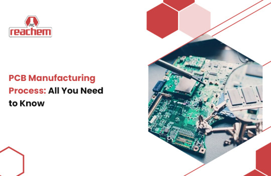
PCB Manufacturing Process: All You Need to Know
Creating a printed circuit board (PCB) is a systematic process that begins with meticulous design and material selection, crucial for ensuring functionality and durability. The initial steps involve the application of a thin layer of copper over a substrate material, typically a fiberglass substrate reinforced with epoxy resin and glass fiber, which provides the necessary rigidity and electrical insulation. This copper layer is then patterned to form conductive areas that will eventually carry electrical signals.
The layout design process utilizes advanced CAD software for precision, ensuring that the conductive paths and component placement areas are accurately defined. Once the design is finalized, it's transferred onto the PCB using photo reactive chemicals and UV exposure, a process known as outer layer imaging. This method allows for the precise alignment of layers and the creation of intricate circuit patterns.
After the design transfer, the excess copper is removed through a careful etching process, leaving behind the copper traces that form the circuitry. The PCB then undergoes a laminating process to apply a solder mask, a protective layer that covers the entire board while exposing the areas where components will be soldered. This solder mask application is crucial for preventing short circuits and ensuring the longevity of the PCB.
Following the application of the solder mask, a silkscreen printing process adds labels and markings to the PCB, aiding in component placement and board identification. The final step in the fabrication processes involves applying a surface finish, such as tin plating, to protect the exposed copper and ensure a reliable soldering surface. Other surface finishes like HASL (Hot Air Solder Leveling) or ENIG (Electroless Nickel Immersion Gold) are also used depending on the application requirements.
Throughout the PCB manufacturing process, precision is maintained through the use of technologies like CNC machines for accurate drilling of holes that will accommodate electronic components. Each part of the PCB fabrication process, from the initial design to the final surface finish, is critical to enhancing the PCB's electrical performance and longevity.
The final stages of assembly involve the placement of components onto the PCB, often by a contract manufacturer specializing in PCB assembly. This is followed by soldering, which can be done through various methods, to securely attach the components to the board.
Rigorous electrical tests are conducted to validate the PCB's performance, ensuring that it meets stringent quality standards before integration into electronic devices. These tests verify the integrity of the conductive paths, the correct orientation of components, and the overall functionality of the PCB.
This holistic approach underscores the importance of meticulous craftsmanship and thorough quality assurance in producing reliable PCBs that power our modern gadgets effectively. Each step, from the initial plating process to the final surface finishing, contributes to enhancing the PCB's electrical performance and longevity, making it a vital component in the electronics industry.
To read more please visit:
Reachemical chemicals
16479857177
600 Matheson Blvd W Unit 5, Mississauga, Ontario ,ON L5R 4C1.
#thin layer of copper#plating process#excess copper#laminating process#tin plating#fabrication processes#substrate material#exposed copper#solder mask application#circuit board manufacturing process#conductive areas#surface finish#layer alignment#outer layer imaging#parts of the pcb fabrication process#epoxy resin and glass fiber#contract manufacturer#outer layers#electrical tests#photo reactive chemicals
0 notes
Text
Pcb Solder Pallet Materials Suppliers- jatmaterial

Looking for dependable sources of PCB solder pallet materials suppliers? Look no further! There are numerous reputable suppliers offering top-quality materials tailored to meet your soldering requirements. These suppliers specialize in providing a diverse range of options suitable for various PCB applications, ensuring durability, reliability, and optimal performance.
When procuring PCB solder pallets materials suppliers, it's crucial to consider factors like material composition, thermal resistance, and compatibility with your unique soldering processes. Luckily, numerous suppliers provide a diverse range of options tailored to meet various requirements and preferences.
These providers have everything you need, whether you're searching for innovative ideas, premium supplies, or a variety of solder pallet options. They are renowned for their commitment to excellence and their skill in meeting the industry's exacting requirements with their product deliveries.
Assuring the consistency and quality of your soldering processes by collaborating with a reputable provider will ultimately improve the dependability and caliber of your output. Furthermore, collaborating with trusted suppliers brings advantages like technical assistance, tailored solutions, and prompt delivery.
#pcb#pcb solder#solder pallet#pcb manufacturer#pcb supplier#pcb solder pallet#psc solder material#pcb solder pallet material supplier
0 notes
Text
double sided pcb manufacturer
Techno Advance System is a largest PCB Assembly Company in India. We offer PCB Assembly, LED PCB Assembly, double sided pcb, and LED Assembly in Ahmedabad, India.
#double sided pcb#double sided pcb manufacturer#double sided pcb in india#pcb soldering manufacturer#double sided pcb manufacturing#double sided pcb in gandhinagar
0 notes
Text

Bare CPU Printed Circuit Board for the Alpha NT XL366 workstation I designed back in 1995 or so. This was an obscure model of an obscure product line, made by a company (Digital Equipment Corp.) that is now itself obscure. To be honest I don't even remember much about this machine now.
What I do remember is the HUUUUGE fight I got into with our Signal Integrity team while I was designing this, over decoupling capacitors.
Decoupling caps are small components that hold a charge to help even out power when a circuit is active. This board featured hundreds of them, smaller than a grain of rice (see photo comparison of mounting pads vs rice grain below).
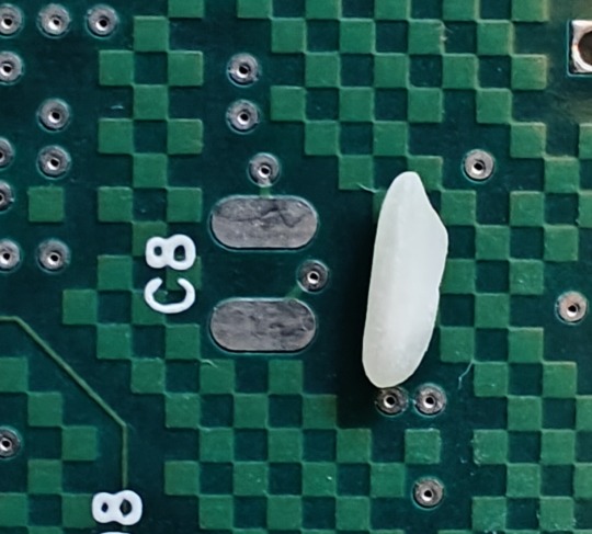
Our Signal Integrity team was tasked with making sure everything was electrically stable, so they required many hundreds of these to be added to the board, based on power simulations they did. Trouble was, they wanted so many, we couldn't even build the board.
My job as the Systems Engineer here was to meet the requirements from the SI team, but also from manufacturing, and the requirement that my PCB layout techs don't go insane trying to place and route the board. SI really only cared about signal quality, so they would not relent, and I ended up getting shouted at at one point by a junior SI engineer who was also under a lot of stress, when I said "There are different schools of thought on this.." and he screamed THERE ARE NOT DIFFERENT SCHOOLS OF THOUGHT ON THIS!!
It got to the point where the product was not going to get built, because we just couldn't fit like a thousand of these tiny caps on the board, we needed to ditch at least 25% of them to have a hope. The models were the models though, and you couldn't argue against them.
But then my boss got a genius idea. What if we could prove the simulation models were too conservative? We came up with an experiment where we would remove caps from an older system and measure the power supply noise, to see how many caps could be taken off before the system became unstable.
Me and the junior SI engineer were tasked with doing this experiment (later deemed The Decapitation Project), so we grabbed a Tektronix scope and Metcal soldering station and headed over to this abandoned lab we had in our old Maynard headquarters, a now creepy attic space on the 6th floor of an old mill building. Here were a few older Alphastation 3000 workstations we built years earlier, working but waiting to be recycled.
We had this special program that would thrash the CPU within an inch of its life, to put a big demand on the power supply system. While this was running, the SI engineer measured the power quality, while I proceeded to (very carefully to avoid short-circuiting the system) actually desolder caps from the board while the workstation was running.
We managed to get about 1/3 of them off before there was any noticeable effect, and we found one specific type of cap was not doing much of anything at all. We took the data back to the head of the SI team, and he finally relented and let us remove several hundred capacitors. (He also buried the report and data I had, because he didn't want the bad publicity - I remember being mad about that)
The system got built after that, and worked just fine. We did try to enact a small bit of petty revenge on the SI team manager though - there was a recognition event for people involved on the project, and me and our PCB procurement guy decided to give the SI team manager a special "Faraday Award" for achievement in capacitance (Farads are a measure of capacitance - geeky eng joke). We took an old bowling trophy with a giant, beer-can sized electrolytic capacitor strapped to the top of it as the award. He was a no-show so we didn't get to present it. Those SI guys never did have much of a sense of humor.
Anyway, long story sorry. Just thinking of it recently because I was helping someone at work with an analog simulation and I remembered this..
497 notes
·
View notes
Text
finally!! finished the guitar pedal my dad got the kit for like a year and a half ago

i redesigned it from scratch because the construction of the original clone was annoying and i think it’s dumb that guitar pedals sometimes use reverse-polarity power and you’re just supposed to guess, so this one takes either polarity through the same jack.


photographic evidence of how this distortion pedal works! based on the Proco RAT of 70s fame, essentially we just clip the signal peaks to introduce other frequencies, which make up the distortion we hear. the FFT on my scope didn’t show much, but either i didn’t tune it right or the instrumentation is just limited here, because we can see pretty clearly the flattened peaks on the processed signal (2, 3) compared to the input (1).


i learned some things about design for manufacturing (DFM) from this project, not just from the original clone board but also from shortcomings of my own design (it turns out that’s a LOT of wires to manage in that small space). if i did it over, i’d put the pins on a 0.1” pitch grid across the board, probably use larger components, and take more care in choosing the shape of the PCB to fit the enclosure around all the hardware. I might even have split it up into a few tiny boards! just for kicks. i also probably would have soldered wires onto the kick switch at an angle, so that they’re not stressed or bent on their way to their final configurations.


the light pipe in particular was a challenge because it turned out the cap on the pipe was small enough that it would slide all the way through the hole meant for a THT LED. I could have fixed this with a washer if I had one, but I eventually hot glued a nut to the cap and let it be.

big thanks to my friends and partners including @thinkpadt530 who helped me with this! i learned a lot from them all, and definitely would not have finished without them. <3
7 notes
·
View notes
Text
Ultimate Guide to PCB Testing Methods: Ensuring Quality and Reliability in Your Circuits
In the electronics sector, Printed Circuit Boards (PCBs) are the life-lines of virtually all gadgets that are in use in the modern society. From humble home appliances to gigantic industrial equipment, PCBs are the skeletal framework of hardware organization and connection of circuit elements. It is vital to guarantee the quality and dependability of these fundamental parts – thus enters PCB testing methods. It is our hope that this extensive hand will help identify the most suitable test strategies for PCB testing, why these techniques matter, and how to maximize your circuits’ functionality.
Introduction

Firstly, an increase in the capability of different electronic devices leads to higher necessary requirements to the PCBs used in their production. Performing tests on the PCBs is an essential step in the manufacturing process done to confirm that a given board performs as a unit to the expected levels. This guide aims at explaining various techniques of PCB testing with a view of having a better understanding on how to achieve quality and reliability on the circuits.
Why PCB Testing is Crucial

PCB Testing When it comes to the potential defects on PCBs, there are shorts, opens, and some component placements. They can cause device failure, decline in performance level, and sometimes also pose safety issues. Through high-quality testing regimes, it becomes easier to address problems before they reach the customer, and thus manufacturers will have reliable and efficient products. Key reasons for PCB testing include:
Detecting Manufacturing Defects: Solder bridges, missing and placed in wrong position components, all can be detected in the initial stages easily.
Ensuring Functionality: Ensuring that the PCB does what is wanted and needed when it is in use, and under several conditions.
Quality Assurance: Ensuring that the business meets industry standards, and what clients require of them.
Cost Efficiency: Decreasing the likelihood of rework and recall by identifying possible defects before they get to the customer.
Types of PCB Testing Methods
These are the types of PCB Testing Methods:
Visual Inspection

Technique one as also referred to as the VI or visual inspection is the simplest and basic type of testing done on PCBs. The technique entails inspecting the board with naked eyes for some of the common faults including solder bridges, missing parts, and misalignment issues.
Automated Optical Inspection (AOI)

AOI employs cameras and software algorithms to check PCBs for defects and performs the inspections singly. This method of inspection is far more efficient than the manual inspection and simultaneously versatile enough to identify numerous problems.
X-ray Inspection

Some functions which include examination of features of BPCs that could not be easily inspected include solder joints under components through x-ray inspection. It is especially effective in inspecting defects in BGA (Ball Grid Array) and other various packages as well.
In-Circuit Testing (ICT)
ICT entails applying different voltage across the PCB to checks on the electrical characteristics of the needy part and connections. The use of this method is highly recommended for the identification of functional problems and verification of the circuit’s goodness.
Functional Testing (FCT)
Functional testing evaluates the effectiveness of the PCB pointing to the fact that it can be tested when placed in use. This method enables the certification of that the PCB works as expected under actual environment.
Flying Probe Testing
In flying probe testing, the probes are moved around to test the electrical properties of the created PCB. Lower to medium volume production runs can be made easily by using this technique; hence it is advantageous in this regard.
Boundary Scan Testing
Boundary scan testing also called as JTAG testing extends test circuitry into all the components for testing the connections between them. Although, this method is very efficient for identifying connection problems and faults.
Burn-In Testing
Burn-in testing puts the PCB in a state of operational stress for a long time to capture early-life failures. This aspect makes the method reliable for the long term since it is likely to identify problems that may occur when the equipment is in use for a long time.
Detailed Analysis of Each Testing Method works
These are the detailed analysis of each testing method works:
Visual Inspection
Pros:
Simple and low-cost
Determined to be a system for the reporting of noticeable defects as soon as they are observed.
Cons:
Time-consuming for complex boards
Limited to visible defects
Automated Optical Inspection (AOI)
Pros:
Fast and accurate
Is capable of detecting various kinds of defects.
Non-destructive
Cons:
High initial setup cost
May need to have better settings optimized for specific boards.
X-ray Inspection
Pros:
Examines hidden features
Ideal for complex packages
Cons:
Expensive equipment
Requires skilled operators
In-Circuit Testing (ICT)
Pros:
Thorough electrical testing
High fault coverage
Cons:
Requires custom fixtures
Not for all the boards or servers that you wish to build.
Functional Testing (FCT)
Pros:
Ensures real-world performance
Detects system-level issues
Cons:
Time-consuming
The mathematical test object can involve complex arrangements of test configurations.
Flying Probe Testing
Pros:
Flexible and adaptable
Cost-effective for small batches
Cons:
Slower than ICT for big volumes
Applicable only when the board is specially designed
Boundary Scan Testing
Pros:
Interconnections have high fault coverage.
Said; No need to have physical access to the test points
Cons:
Requires boundary scan-enabled components
Complex setup
Burn-In Testing
Pros:
Identifies early-life failures
Ensures long-term reliability
Cons:
Time-consuming and costly
Perhaps stressful to the board
Choosing the Right Testing Method
The choice of the appropriate method of PCB testing can be influenced by several factors such as the level of complexity of the PCB and the numbers of boards to be tested as well as the actual costs of the testing process and other features. Consider the following when choosing a testing method:
Board Complexity: Great board densities or component placement can be a determinant as to whether one needs AOI or X-ray inspection.
Production Volume: Applications that are characterized by high volumes can be easily facilitated by ICT while the low to medium volume applications may require flying probe testing.
Budget: Both manual inspection and AOI are favorable for various production volumes, while X-ray and ICT are more expensive at the beginning.
Specific Requirements: There are two types of the test, namely Functional Test and Burn-In Test that should be made so as to attain the long term reliability in applications that are critical.
Best Practices for PCB Testing
Using the best techniques in testing PCBs increases the quality and reliability of the circuits that you are working on. Here are some key practices to follow:
Early Testing: It is recommended to carry out the tests when the product is still in its design and manufacturing phase so that problems can be noted earlier before they reach a very catastrophic level.
Automate Where Possible: Use method such as automation to reduce the time and improve on the quality of the testing.
Regular Calibration: It is necessary to check if all the testing equipment used for calibration are accurate.
Comprehensive Coverage: This way, you will be able to ensure that there are no defects that are not tested as the best testing approach combines all types of testing methods.
Document Everything: Ensure that you keep records of the tests performed, the results obtained, as well as any measures taken to correct the breaches.
Common Challenges and How to Overcome Them
These are the common challenges and how to overcome them:
False Positives/Negatives
Automated testing methods maybe good some times, they give you the results that are either positive or negative and this will lead to unnecessary rework or more alarming leaving critical defects unfound. In order to avoid this, make sure that testing algorithms and testing equipment are updated and fine-tuned from time to time.
Component Access
Some of the testing techniques involve handling parts of the circuit and with high density board this can be very difficult. Some of the ways in which testbench implementation can be avoided are as follows Boundary scan testing and X-ray inspection.
High Costs
Some form of testing such as X-ray and ICT testing is often very costly. The effectiveness must come with reasonable prices; try to combine some of the mentioned approaches to cover all the aspects without spending too much money.
Future Trends in PCB Testing
About the future, it can be stated that its trends will be in fact linked to the tendencies in technologies and expectations towards ever higher quality and quantity of tested PCBs. Key trends to watch include:
AI and Machine Learning: Using of intelligence algorithms and machine learning in testing algorithms to enhance the efficiency and the minimization of false negative or false positives.
IoT and Smart Manufacturing: Higher testing flexibility and opportunities for the continuous test process supervision.
Advanced Imaging Techniques: The need for better techniques that would enhance the detection of defects within a printed circuit.
Environmental Stress Testing: More focus in the testing of PCBs under different environmental pressures in order to improve on its longevity.
Conclusion
Quality and reliability of packaged circuits have to be maintained to contribute positively in any electronic equipment. This paper seeks to explain the common testing techniques for PCB so that PCB manufacturers are able to test and see if they are free from defects and if they are functional. This ultimate guide will give you a full insight on the available options in PCB testing that will enable you make the best decision that will give you perfect circuits.
The aim is to help you understand how to attain the best quality of PCBs, what methods are worth following, and what trends drive future improvements, thus contributing to the quality of the final electronic products and, consequently, consumer satisfaction.
#PCBTesting#Electronics#CircuitBoard#QualityControl#Engineering#Technology#Manufacturing#IndustrialDesign#Tech#Innovation
2 notes
·
View notes
Text
Just How Carries Out A PCB Assembly Procedure Job?
The PCB assembly process begins with PCB fabrication, adhered to by part purchase. Parts are then put on the board utilizing automated pick-and-place devices. Solder insert is applied to connection parts during the course of reflow soldering. Inspection methods like AOI as well as practical testing ensure quality. Finally, panels are packaged for delivery after passing QC checks.
4 notes
·
View notes
Text
In today’s fast-paced industrial landscape, automation and smart technology are revolutionizing manufacturing and logistics. One such transformation is happening in roller conveyor operations, thanks to the Internet of Things (IoT). As industries strive for efficiency, IoT-enabled roller conveyor systems are optimizing workflows, reducing downtime, and enhancing productivity. Companies like Yontro Mechatronic Systech are at the forefront of this revolution, offering innovative solutions to modernize conveyor operations.
#Conveyor Belt Manufacturers in India#Wave Soldering Machine#Reflow Soldering Machine#Industrial Work Station#Roller Conveyor#Roller Conveyor System#Flat Belt Conveyor#Assembly Conveyor#Inclined Conveyor Belt#Cleated Belt Conveyor#Truck Loading Conveyor#Telescopic Belt Conveyor#PCB Assembly Machines
0 notes
Text
Printed Circuit Board Basics
Most of us are using Printed Circuit Board in our daily life. Printed Circuit Boards are used in almost all the Electronic products, from consumer gadgets such as PCs, tablets, smartphones, and gaming consoles to industrial and even high tech products in strategic and medical electronics domains.
Here, we have some statistics for you that shows how many electronic devices connect worldwide from 2015 to 2025. This statistic shows an increase in the use of a number of PCB in people daily life. Hence, CircuitWala took this opportunity to provide a basic knowledge about PCB via this article.
There are so many books available online which teach about Printed Circuit Board design and hardware part. There are few links available online which shows only a few basic fundamentals of PCB and few are there for Basics of Printed Circuit Board (PCB) Design. Few which gives good know knowledge on Printed Circuit Board terminology. But in the end for the hobbyist, there is no such material available which make their work easy.
Now days there few online designing websites available which allow hobbyist and students to create their design and Printed Circuit Board fabrication part. These websites provide limited features and charge high for the full edition. We, @CircuitWala are in try to provide one platform which provides plenty of Printed Circuit Board knowledge digitally to make your work simple and easy.
Alternatives of PCB include wire wrap and point-to-point construction. Creating a layout of PCB is a little bit time-consuming method as compared to its alternative solution but manufacturing of PCB is cheaper and faster then other wiring methods as electronic components are mounted and wired with one single part.
Let’s start with some basics of Printed Circuit Board with this article. Here in this article we will discuss about history of PCB to understand the emerge of PCB, Types of PCB to make your complex PCB a very simple using different types, Usage of PCB to provide you an idea to create more Printed Circuit Board projects, Advantages and Disadvantages, Possible Future to know about new technological change in Printed Circuit Board manufacturing and also about how to destroy and manage your PCB’s e-waste? We know you are eager to know all the stuff in details but before that let’s make a simple definition of Printed Circuit Board.
What is Printed Circuit Board?Printed Circuit Board is an electronic device made of conductive material(FR-4) like copper which connects components mounted on it to to get desired output by providing an input on another end.
When the board has not mounted with any of the components is called as Printed Circuit Board or Printed Wired Board. Mounting of an electronic component on Printed Circuit Board is called as PCB assembly.
History of Printed Circuit BoardThe invention of Printed Circuit Board was by Austrian engineer Paul Eisler as part of a radio set while working in England around 1936.
In early days before Printed Circuit Board became common in use, Point-to-Point construction was used. This meant some bulky and unreliable design that required plenty of sockets and regular replacement of it. Most of this issue directly address when PCB went into regular production.
Originally, every electronic component had wire leads, and the PCB had holes drilled for each wire of each component. The components’ leads were then passed through the holes and soldered to the PCB trace. This method of assembly is called Through-Hole construction. There is one other method to mount component is called as Surface Mount.
Type of Printed Circuit BoardPCBs are produced from the different types of material and on the basis of that material PCBs are divided mainly into two parts: Rigid PCB and Flexible PCB. Nowadays, a combination of Rigid and flexible PCB is also possible and that is called as Flexi-Rigid PCBs.
Most of the PCBs are built in layers. The inner layer is the base material called as a substrate. Rigid PCBs are mainly made of material like epoxy materials and Flexible PCBs are made of plastic material that can withstand high temperatures.
Rigid PCBs are generally, hard materials that hold the component in a better way. The motherboard in the tower of a computer is the best example of Rigid PCBs. Flexible PCBs fundamental material allows PCB to fit into forms that Rigid PCBs can not. Flexible PCBs can turn round without harmful the circuit on PCB.
All Rigid and Flexible PCBs can come in three formats by layers: Single Layer, Double Layer, and Multi-Layer.
1. Single Layer PCBSingle Layer PCBs have been around since the late 1950s and still dominate the world market in sheer piece volume. Single Sided PCBs contain only one layer of conductive material and are best suited for low-density designs. Single-sided PCBs are easy to design and quick to manufacture. They serve as the most lucrative platform in the industry.
2. Double Layer PCBDouble Layered printed circuit board technology is conceivably the most popular type of PCB in the industry. Double Sided PCB (also known as Double-Sided Plated Thru or DSPT) circuits are the gateway to advanced technology applications. They allow for a closer (and perhaps more) routing traces by alternating between top and bottom layers using vias.
3. Multi Layer PCB
Multilayer PCB is a circuit board that has more than two layers. Unlike a Double-Sided PCB which only has two conductive layers of material, all multilayer PCBs must have at least three layers of conductive material which are buried in the center of the material.
Usage of Printed Circuit BoardBy reading this article till this point, we hope that you are now able to get about printed circuit boards. Now, we will make you understand about different applications of printed Circuit Board.
In this digital world, Printed Circuit Board is in almost all our daily life electronic devices and in our industrial electronics as well. Below are the industries where PCBs are used:
Possible FutureNowadays, most of the circuits are replaced to produce Printed Circuit Board from the old methods. Revolution in technology made many of the processes automated and hence it is easy to manufacture PCB. But still, these processes are a bit expensive to hire, involve toxic waste and use high temperatures and acids. With technological advances we have seen in the past years, it is not hard to imagine PCB will soon be revolutionized. Not only that but research institutes predict a more ‘green’ future for PCBs; PCBs being made of paper.
Electronic Waste (e-waste)Electronic Waste or e-waste is described as discarded electrical or electronic devices. Informal processing of e-waste in developing countries can lead to adverse human health effects and environmental pollution.
Electronic scrap components contain a hazardous substance such as lead, cadmium, beryllium, or brominated flame retardants. Recycling and disposal of e-waste may involve significant risk to health of workers and communities in developed countries and great care must be taken to avoid unsafe exposure in recycling operations
Nowadays, developing countries are encouraging electronic users to take care while recycling the e-waste or submit them to the organization who are involved in such activities.
SummaryIn this blog, we have learned the basics of Printed Circuit Board. CircuitWala is planning to write as many blogs to provide more and more knowledge of Printed Circuit Board. Either it is basics or manufacturing or usages or advantages and disadvantages of PCBs. We will also try to make our users/customers up to date for the new technology innovations, including past histories and revolution of the PCB industries.
In the next blog, we will look at more briefly about the different types of Printed Circuit Board. We also understand the process to make it and different usage and application for the same.
#electronic circuit design company#pcb circuit manufacturer in ahmedabad#pcb design & manufacturing services#printed circuit board companies#printed circuit board order online#PCB manufacturer#Printed Circuited Board#double layer PCB#PCB Quality Control
2 notes
·
View notes
Text
Circuit Board, PCB assembly & electronics manufacturing service provider from China (hitechcircuits.com)
What is a prototype PCB assembly?
PCB prototyping is the experimentation pilot stage of the product which is to be mass produced at a later stage. This is more of an experiment which is done after the initial discussions and the design. This offers a pre-production analysis of the boards that are to be manufactured, reducing the possible number of errors in the PCB design. PCB prototypes help the manufacturer analyze the strengths as well as weak areas of their proposed circuit boards. Prototypes also serve as a reference point for future versions of the same product. At Hitechpcba, we handle PCB prototype assembly in quantities from one to hundred printed circuit boards.
We have acquired capabilities that enable us to serve our clients better. All these years, we have worked on many complex prototype PCB assembly projects, and we believe the following capabilities have helped us serve our clients better.
Prototype PCB Assembly Services: We specialize in the following prototype printed circuit board assembly services.
SMT: We can provide single-sided and double-sided surface mount PCB assemblies in different specifications.
Plated Through Hole: We offer plated through hole assembly with selective soldering.
Mixed Assemblies: We often work on projects involving mixed assemblies – through-hole and SMT and electromechanical assemblies.
PCBA Testing: All the PCBA functional testing is performed in-house. Over the years, we have invested in various test fixtures and equipment, which helps us ensure the quality of PCBA. Currently, we provide the following types of PCBA testing services:
Flying probe testing for PCB
Functional testing including system and board-level testing
General PCB Assembly Capabilities: Our general PCB assembly capabilities are not limited to these:
RoHS, leaded or lead free, clean and no chemistries
PCB components including various types of QFNs, BGAs, 0105, 0201, 0804, and press fit components in small quantities.

What are the benefits of a prototype PCB assembly?
Prototype PCB assembly comes with several advantages. These benefits play a major role in the facilitation of your PCB manufacturing. Some of these benefits include:
Detection of Flaws Early
With prototype PCB, you will easily detect whatever flaws are present during the product’s development stages. This will allow you to solve the issues thereby saving you some money if you had gone ahead to make the production having the flaws in them.
If you go ahead to make changes during the production, there may be a need for more technicalities, and this may be expensive.
Testing of Each Component
With a prototype, you will be able to test all your system’s elements individually before you go ahead to set it up. You should do this because it is important especially for very complex projects composed of several parts that are PCB based.
When you validate each of these components, you will be able to identify those areas having issues that you should look into. This is the only way the project can function the right way.
Reduction in Total Costs
Utilizing the prototype bare PCB for any of your projects could go a long way in reducing what you’ll have spent in total for the project. With prototyping, you will be able to notice those errors in your project and then make corrections before you start the real production.
As soon as these flaws have been checked and rectified, then you may continue with the manufacturing of your Printed circuit boards in large quantities, thereby saving you unnecessary costs.
High-Quality PCBs
Why prototyping your PCB is important is to help you test if your project will function effectively. When we talk of testing, it involves the identification of errors present and then rectifying and making corrections to them.
Therefore, the eventual PCB after the prototyping will be of high quality that surely meets standards set internationally.
Less Turnaround Time
With prototype PCB assembly, you will be able to reduce the total time used in producing your printed circuit board. While making use of prototype printed circuit boards, you’ll be able to see the errors and then make corrections before you start the actual production.
Therefore, the eventual prototype will be free of defects. This implies that your PCBs will be produced quickly by your manufacturer.

What are the different types of prototype PCB assembly services you offer?
With years of market presence and experience, we specializes in the following prototype PCB assembly services.
Plated through-hole (PTH): We can provide the through-hole assembly with selective soldering.
Surface mount technology (SMT): We offer single-sided as well as double-sided SMT board assemblies in varied specifications.
Mixed Assemblies: Our experts often work on projects involving both PTH and SMT assemblies.
What are the types of testing Hitechpcba use for prototype PCB assembly?
Automated Optical Inspection (AOI): This is performed before and after the soldering to identify the component placement, presence, and solder quality.
X-ray Testing: In this type of testing, the operator relies on the X-ray images of the PCB to check the solder joints and lead-less components such as Quad Flat Packs and ball grid arrays, which are generally not visible to naked eyes.
In-Circuit Testing (ICT): This method is used to detect manufacturing defects by testing the electrical properties in the SMT Assembly.
These techniques help us ensure the reliability and accuracy of the circuit boards. In addition to this, it ensures a long operational life of equipment, minimal production losses, streamlined processes, and much more.
What are the capabilities Hitechpcba offer for prototype PCB assemblies?
We specialize in offering IPC compliant, and quick turn PCB assemblies. We are very particular about our scheduled deliveries and timelines, and we deliver without compromising the quality. Our PCBA capabilities are not limited to these. Here are some capabilities we offer through prototype PCB assemblies.
RoHS compliance
Stringent testing procedures
Device encapsulation
Full turnkey, partial turnkey, and kitted/consigned services
Assemblies using Surface Mount (SMT), Thru-hole, Mixed Technology (SMT/Thru-hole), Single and double-sided SMT/PTH, Large parts on both sides, BGA on both sides.
Do you perform a component analysis for prototype PCB assemblies?
Yes, we check the quality and performance of components before mounting them on the circuit boards. This is because a malfunctioning component can affect the performance of the entire circuit board assembly and also pose risks.
What is your standard turnaround time for a prototype PCB assembly?
Our turnaround time for standard applications is two weeks. This timeframe varies depending on the complexity of the applications. However, we are committed to offering quick turnaround times without compromising on quality, functionality, and accuracy, which offers our client a competitive advantage and reduced time to market. You can also request any emergency assistance or queries related to any type of PCB assembly. Our experts will assist you in all possible ways.
How is the cost of prototype PCB assembly estimated?
PCBA costing varies based on the different factors, such as PCBA parts, type of materials to be used, order quantity, and much more. We can also offer quotes and customization options once you share the detailed requirement with us.
We focus on quality and customer satisfaction over anything else. This has helped us build a long list of happy and satisfied customers. So, if you wish to partner with a manufacturer of prototype PCB assembly in China, then don’t hesitate to reach us. Our experts will assist you through all the phases of the prototype PCB assembly process. We look forward to making your experience with us better and memorable.
How to choose prototype pcb assembly manufacturer?
Our pcb prototype assembly service includes the sourcing of components. This allows you to concentrate on what you do best: layout design. We have a dedicated sourcing staff that coordinates with multiple suppliers and distributors to purchase electronic parts as per client requirements, and our staff completes these purchasing particulars in a most efficient manner. We have advanced processes for optimal selection of packaging (cut tape, tube, bulk, etc.) to reduce the total cost. Furthermore, we are capable of cross-referencing parts and even locating hard-to-find and obsolete parts. Customers can be rest assured that when Hitech Circuits substitutes components that they are high quality: we only use the electronic component numbers and manufacturers specified in the BOM. We will not modify your original layout design. Part substitutions take place only with your permission.
The final pcb prototype assembly service cost includes assembly labor charges, bare circuit board rates, and part costs. We understand the importance of prompt delivery. The sooner the components are sourced, the sooner we can begin circuit board fabrication. We thoroughly evaluate engineering inquiries and concerns related to the related parts with our clients before commencing circuit board assembly. The average time taken for pcb manufacturing assembly is about two weeks, which can be further reduced if there are no hard-to-locate components or documentation mistakes.
We have specialized experts to deliver fast turnarounds for prototype circuit board assembly with surface-mount (SMT), through-hole (THT) and mixed-technology components.
Anyone interested in electronics and electronic circuit boards needs to understand the various stages of developing and producing a printed circuit board. It can come in handy when you are seeking a top prototype smt assembly provider. The various production stages of printed circuit boards entail design, prototyping (prototype PCB development and rapid prototyping pcb assembly), and PCB high volume production. Different entities will always seek part of the whole production process depending on their electronic circuit board needs.
However, this article seeks to help you understand everything about prototype PCB assembly, a fundamental aspect of the PCB production process.
Rapid prototyping pcb assembly represents a fundamental phase of the printed circuit production process. It is also inferred as PCBA prototype assembly, SMT or surface-mount technology PCB prototype, PCB sample assembly, etc. From these alternative names, the meaning of prototype assembly regarding printed circuit boards becomes apparent. So what is assembly prototype?
PCB prototype assembly service is a fast prototype printed circuit board assembly primarily used to test fresh or new electronic designs. Consequently, it assists with checking and ensuring quality assurance of the PCB. For instance, it verifies that no bug exists in the test PCB, updates the design, and finds bugs. In most instances, prototype assembly of an electronic project will require two or three iterations to ensure everything is perfect.

Why Choose Hitech Circuits PCB Assembly for Your Prototype PCB Assembly Projects?
There are several PCB manufacturers specializing in prototype PCB assembly services. However, Hitech Circuits stands out owing to the following:
1.Strong Supply Chain: Over the years, we have built strong supply chain relationships in the industry, which helps us fulfill the requirements of turnkey prototype assembly services easily.
2.Fastest Turnaround Times: Our engineering expertise coupled with our understanding of industry requirements and a well-equipped facility enables us to assure the fastest turnaround times of 24-48 hours.
3.Reliability: All the printed circuit boards that we produce are IPC compliant, which helps us assure reliability.
4.Competitive Pricing and Quick Quote: Our supply chain relationships enable us to assure competitive prices. The cost of the PCB prototype assembly will be made available within 24-48 hours.
2 notes
·
View notes
Text
What is PCB Assembly ?
PCB Assembly manufacturer - Hitech Circuits Co., Limited
It’s the step in the manufacturing process in which you populate a blank board with the electronic components needed to make it into a functional printed circuit board. It’s these components that make a board into the circuit that enables an electronic product to function. PCB assembly typically takes place via one of two processes:
1. Surface-mount technology
SMT: SMT stands for “Surface Mount Technology“. The SMT components are very small sizes and comes in various packages like 0201, 0402, 0603, 1608 packages for resistors and capacitors. Similarly for Integrated circuits ICs we have SOIC, TSSOP, QFP and BGA.
The SMT components assembly is very difficult for human hands and can be time taking process so it is mostly done by automated pick and place machine.
2. Through-hole manufacturing
THT: THT stands for “Through hole Technology”. The components with leads and wires, like resistors, capacitors, inductors, PDIP ICs, transformers, transistors, IGBTs, MOSFETS are example.
The component has to be inserted on one side of PCB and pulled by leg on other side and cut the leg and solder it. The THT components assembly is usually done by hand soldering and is relatively easy.
Printed Circuit Board Assembly Techniques
There are only two common PCBA techniques available for use by a PCB designer. The methods are:
1. Automated PCB Assembly Techniques
Generally, this technique employs the use of state of the art machines, which are fully automatic. For example, the surface mount components are worth positioning with the aid of an automated pick and place machine.
Again, reflow soldering is commonly for surface mount components usually done in a reflow oven. An automated solder stencil is also used to apply the solder paste on the PCB.
Finally, high tech inspection machines are used to confirm and check the quality of the PCBA. Some of which include: Automated optical inspection machine (AOI), X-ray inspection machines, etc.
Above all, due to the precise monitoring, control of soldering, no human input and versatile machines.
This technique ensures utmost efficiency, output consistencies, and limits defects.
2. Manual PCB Assembly Techniques
This method is favorite for use with through-hole parts, which needs manual placement on the board. Besides, with these through-hole parts, it’s advisable you use wave soldering. Note that in the through- hole assembly process, you need to place the components and electronics on the PCB.
After that, you use wave soldering to solder the leads. Typically, you will need an individual to insert a component into a marked PTH. Once done, transfer the PCB to the next station where the next person will be on standby tasked with fixing another part.
What are the Benefits of SMT PCB Assembly?
SMT assembly provides many benefits and some of them are as follows:
It can be used to incorporate small components.
In SMT, the components can be placed on both sides of the board.
It assures high component densities.
Fewer holes need to be drilled for surface mounting than through-hole.
It require low initial costs and time for setting up the mass production.
SMT is the simpler and faster-automated assembly when compared to through-hole.
Errors regarding the component placement can be easily rectified.
Surface mount PCBs feature strong joints, which can easily withstand vibrations.
What are the techniques used in Surface Mount Technology?
There are several techniques for the reflow process. After applying the solder paste or a flux mixture on the board and after placing the components, the boards are conveyed to a reflow soldering oven. The techniques used for reflowing soldering include infrared lamps, hot gas convection, fluorocarbon liquids with a high boiling point, and so on.
What are the different testing methods used in SMT PCB Assembly?
Hitech Circuits as the PCB assembly manufacturer, we perform the following testing and inspection to ensure the quality of surface mount PCBs.
Automated Optical Inspection (AOI): This is performed before and after the soldering to identify the component placement, presence, and solder quality.
X-ray Testing: In this type of testing, the operator relies on the X-ray images of the PCB to check the solder joints and lead-less components such as Quad Flat Packs and ball grid arrays, which are generally not visible to naked eyes.
In-Circuit Testing (ICT): This method is used to detect manufacturing defects by testing the electrical properties in the SMT Assembly.
What type of files or documents should I send for SMT PCB Assembly?
Gerber Files: The file contains all details of physical board layers including solder masks, copper layers, drill data, legends, and so on.
Bill of Materials (BOM): This contains information on the list of items needed for the PCB manufacturing and the instructions of manufacturing.
Pick and Place File: This file contains information on all components to be used in the PCB design and their rotation and X-Y coordinates.
The whole process of PCB Assembly
1. Bare board loader machine
The first step in the PCB assembly is to arrange the bare boards on the rack, and the machine will automatically send the boards one by one into the SMT assembly line.
2. Printing solder paste
When PCB on the SMT production line, firstly, we have to print solder paste on it, and the solder paste will be printed on the pads of the PCB. These solder pastes will be melt and solder the electronic parts to the circuit board when it passes through the high-temperature reflow oven.
In addition, when testing new products, some people will use film board/adhesive cardboard instead of solder paste, which can increase the efficiency for adjusting the SMT machines.
3. Solder paste inspection machine(SPI)
Since the quality of solder paste printing is related to the quality of welding of subsequent parts, some SMT factories will use optical machine to check the quality of solder paste after printed the solder paste in order to ensure stable quality. If there any poorly printed solder paste board, we will wash off the solder paste on it and reprint, or remove the excess solder paste if there is redundant solder paste on it.
4. High speed SMT machine
Usually, we will put some small electronic parts (such as small resistors, capacitors, and inductors) to be printed on the circuit board first, and these parts will be slightly stuck by the solder paste just printed on the circuit board, so even if the speed of printing is very fast and the parts on the board will not fall away. But large parts are not suitable for use in such high speed SMT machines, which will slow down the speed of small parts assembly. And the parts will be shifted from the original position due to the rapid movement of the board.
5. Universal SMT machine
Universal SMT machine is also known as "slow machine", it will be assembled some large electronic components, such as BGA IC, connectors, etc., these parts need more accurate positions, so the alignment is very important. Use a camera to take a picture to confirm the position of the parts, so the speed is much slower than High speed SMT machine we taked before. Due to the size of the components here, not all of them are packed in tape and reel, and some may be packed in trays or tubes. But if you want the SMT machine to recognize the trays or tube-shaped packaging materials, you must configure an additional machine.
Generally, traditional SMT machines are using the principle of suction to move electronic parts, and in order to place the parts successfully, and there must be the flat surface on these electronic components for the suction nozzle of the SMT machine to absorb. However, for some electronic parts don’t have a flat surface for these machines, and it is necessary to order special nozzles for these special-shaped parts, or add a flat tape on the parts, or wear a flat cap for thees electronic parts.
6. Manual parts or visual inspection
After assembled all parts by the high speed SMT machine or Universal SMT machine and before going through the high-temperature reflow oven, and we will set up a visual inspection station here and to pick out the deviation parts or missing components boards etc., because we have to use a soldering iron to repair if there are still defectives boards after passing the high-temperature oven, which will affect the quality of the product and will also increase the cost. in addition, for some larger electronic parts or traditional DIP parts or some special reasons cannot be processed by the SMT machine before, they will be manually placed on pcb here.
7. Reflow oven
The purpose of reflow oven is to melt the solder paste and form a non-metallic compound on the component feet and the circuit board, that means to solder electronic components on the circuit board. The temperature rise and fall curves often affect the soldering quality of the entire circuit board. According to the characteristics of the solder materials, usually the reflow oven will set the preheating zone, soaking zone, reflow zone, and cooling zone to achieve the best soldering effect.
For example, the melting point for SAC305 solder paste with lead-free is about 217°C, which means that the temperature of the reflow oven must be higher than the melting points to remelt the solder paste. What's more, the maximum temperature in the reflow furnace should not exceed 250°C, otherwise many parts will be deformed or melted because they cannot withstand such a high temperature.
Basically, after the pcb passed through the reflow oven, the assembly for the entire circuit board is almost complete. If there are hand-soldered parts, we need to transfer to DIP process, and then we have to check the quality after reflow oven by QC department.
8. Automatic optical inspection(AOI)
The main purpose of setting up AOI is because some high density boards can’t be process the following ICT test, so we used AOI inspection to replace it. But even using AOI inspections, there still have the blind spots for such checking, for example, the solder pads under the components cannot be checked by AOI. At present, it can only check whether the parts have side standing issue, missing parts, displacement, polarity direction, solder bridges, lack of soldering etc., but cannot checking the BGA solderability, resistance value, capacitance value, inductance value and other components quality, so far AOI inspection can’t completely replace ICT test.
Therefore, there is still some risk if only AOI inspection is used to replace ICT testing, but ICT test is also not 100% make sure the good quality, we suggest these two ways can be combined with together to make sure the good quality.
9. PCB unloader machine
After the board is fully assembled, it will be retracted to the unloder machine, which has been designed to allow the SMT machine to automatically pick and place the board without damaging the quality for PCB.
10. Visual inspection for finished products
Normally there will be a visual inspection area in our SMT production line whether there is an AOI station or not, and it will help to check if there are any defectives after completed assembled the pcbs. If there is an AOI station, it can reduce the visual inspection worker on our SMT line, and to reduce the potential cost, and because it is still necessary to check some places that cannot be judged by AOI, many SMT factories will provide the mainly visual inspection templates at this station, which is convenient for visual inspection worker to inspect some key parts and polarity for components.
11. DIP process
DIP process is a very important process in the whole PCBA processing, and the processing quality will directly affect the functional for PCBA boards, so it is necessary to pay more attention to the DIP process. There are many preliminary preparations for DIP process. The basic process is to re-process the electronic components first, like to cut the extra pins for some DIP components, our staff received the components according to the BOM list, and will check whether the material part numbers and specifications are correct or not, and performs pre-production pre-processing according to the PCBA samples. The steps are: Use various related equipment (automatic capacitor pins cutting machine, jumper bending machine, diode and triode automatic forming machine, automatic belt forming machine and other machines) for processing.

12. ICT test
Printed Circuit board open/short circuit test (ICT, In-Circuit Test), The purpose of ICT test is mainly to test whether the components and circuits on the printed circuit board are open or short issues. It can also measure the basic characteristics of most components, such as resistance, capacitance, and inductance values to judge whether the functions of these parts are damaged, wrong parts or missing parts etc. after passing through the high-temperature reflow oven.
ICT test machines are divided into advanced and basic machines. The basic ICT test machines are generally called MDA (Manufacturing Defect Analyzer). It’s just to measure the basic characteristics of electronic components and judge open and short circuits issue we talked above.
In addition to all the functions of the basic ICT test machines, for advanced ICT test machine can also test the whole PCBA by using power, start to testing the PCBA boards by setting the program in the test machine. The advantage is that it can simulate the function of the printed circuit board under the actual power-on condition, this test can partly replace the following functional test machine (Function Test). But the cost for the test fixture of this advanced ICT test can probably buy a car, it’s too expensive and we suggest it can be used in mass production products.
13. PCBA function test
Functional testing is to make up for the ICT test, because ICT only tests the open and short circuits on the the PCBA board, and other functions such as BGA and other fuctions are not tested, so it is necessary to use a functional testing machine to test all functions on the whole PCBA board.
14. Cutting board (assembly board de-panel)
Normally, printed circuit boards will be produced in panel, and it will be assembled to increase the efficiency of SMT production. It means several single boards in one panel, such as two-in-one, four-in-one etc. After finished all the pcb assembly process, it needs to be cut into single boards, and for some printed circuit boards with only single boards also need to cut off some redundant board edges.
There are several ways to cut the printed circuit board. You can design the V-cut using the blade cutting machine (Scoring) or directly manually break off the board (not recommended). For more high density circuit boards, it will be used the professional splitting machine or the router to split the board without any damage the electronic components and printed circuit boards, but the cost and working hours will be a little longer.
Why Choose Hitech Circuits PCB Assembly Manufacturer for Your PCB Assembly Projects?
There are several PCB manufacturers specializing in PCB assemblyservices. However, Hitech Circuits PCB Assembly stands out owing to the following:
Assistance in Material Procurement:
Technically, in PCB assembly services, the quality of parts is the responsibility of the OEM; however, we ease your job by assisting you to make the right selection. We can help you procure all your parts of the same type own a single part number, thanks to our supply chain and vendor network as well as experience. This saves time and cost that goes in ordering single parts as you plan.
Testing procedures:
We are very focused on quality and thus implement stringent testing procedures at each stage of the assembly and after completion.
Fast Turnaround Times:
Our well-equipped facility and the right tools enable us to complete your requirements well before time, and without compromising on the quality or functioning of the PCBs. For simple designs we revert in 24 to 48 hours.
Cost Effectiveness:
While PCB assembly is a cost-effective alternative, we go a step further and assure that the parts you list are of a good quality and suitable for your requirement. Also, you can control the part flow and replenish them as needed. This eliminates the need to buy extra stock and store it.
Quick Quote:
We offer a quick quote based on your BOM. All you need is a detailed BOM, Gerber files, your application requirement sheet, and quantity.
We’re not one to stand still, which is why we use the latest equipment and the finest minds to create your PCB projects. We’re constantly keeping our finger on the pulse of the latest trends. And as a result, we know how to deliver the highest standards of PCB assembly to meet all your requirements.
Our dedicated, friendly customer service team also means that we support you every step of the way. Offering our expert guidance to ensure a complete PCB project that you’re happy with.
Contact us today
No matter what your printed circuit board assemblyneeds are, we always aim to deliver efficient, dependable solutions. For more information about our services, do not hesitate to get in touch with us today for a no-obligation quote
2 notes
·
View notes
Text
【The ultimate guide to choosing the perfect Dry Ice Cleaning Machineand dry ice machine for your needs】
UNDERSTANDING YOUR REQUIREMENTS
1. Determine your application area:
Before diving into machine specifications, determine your primary application. Whether it’s industrial cleaning, food preservation, or special effects in the entertainment industry, understanding your specific use case will allow you to more accurately select the machine that’s best for you.Or you can tell us your needs and we will recommend the best solution for you.
2. Dry ice quantity issue:
Consider the amount of dry ice you need. Industrial applications may require high-capacity machines, while smaller equipment can meet smaller-scale needs. Understanding your production requirements is critical.You can refer to 【Dry Ice Production Demystified: Go Behind the Scenes and Uncover the Magic of Pelletizers】and 【How to set up your own dry ice manufacturing factory?】Learn more about dry ice in two articles.
TYPES OF DRY ICE CLEANERS AND DRY ICE PELLETIZERS
1. Dry ice cleaning machine(Dry ice blasting machine):
Compressed air is used to accelerate dry ice pellets to supersonic speeds and spray them onto the surface being cleaned. The high-speed ice particles hit the dirt, and through the freezing and mechanical action of the ice, the dirt is peeled off the surface.It is widely used for cleaning machinery and equipment, production lines, building surfaces, etc. It is especially suitable for the food and pharmaceutical industries because the cleaning process does not require water or chemicals.(Want to learn more about Dry Ice Cleaning?)
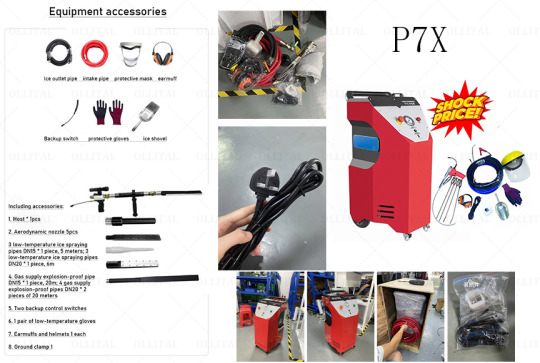
· P7X Dry ice cleaning machine: Very suitable for cleaning carbon deposits and oil stains in car engines. It can effectively complete cleaning without damaging engine parts etc..(Suitable for use in car repair service centers, auto repair shops, home cleaning and maintenance, etc.)Go to view product details
· A625i Dry ice cleaning machine: Suitable for cleaning oily molds, motor windings, paint rust cleaning, and printing machine ink residues etc.. (Suitable for rubber factories, shoe factories, factory machine maintenance, etc.)Go to view product details

· P60 Dry ice cleaning machine: Used for car interior renovation and cleaning, car seat cushions, surface glue residue, and oil stain cleaning etc..(Suitable for use in car repair service centers, auto repair shops, home cleaning and maintenance, etc.)Go to view product details

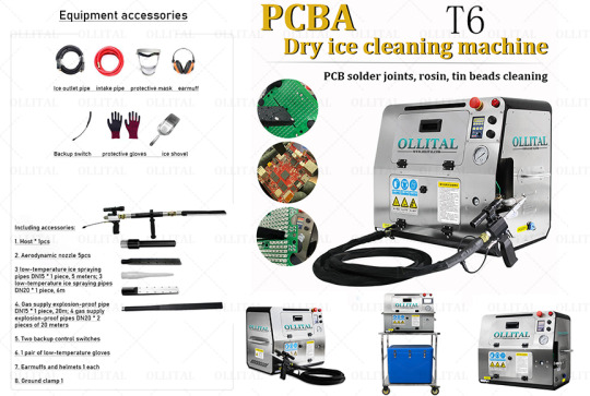
· T6 Dry ice cleaning machine: Used for PCB circuit board renovation and cleaning, soldering residue, surface glue residue, oil stains, PPS material deburring, etc. (Suitable for component factories, component maintenance, factory machine maintenance, etc.)Go to view product details
· B3+ Dry ice cleaning machine: Used for cleaning motor winding dust, printing machine ink, oil sludge, rust stains, heavy oily metal, etc.(Used to clean and maintain a variety of industrial equipment, including engines, pumps, valves, pipes, etc.)Go to view product details
Generally speaking, the dry ice cleaning machine is an efficient, environmentally friendly, and multi-purpose cleaning equipment. Its working principle is based on high-speed spraying of dry ice particles to clean the surface through freezing and mechanical impact. The advantages of this cleaning method include being water-free, leaving no chemical residue, being non-abrasive, suitable for a variety of surfaces and materials, and having a wide range of applications in a variety of industries.
For potential users, when choosing a dry ice cleaning machine suitable for specific needs, factors such as cleaning objectives, working environment, cleaning effect requirements, production capacity and budget need to be considered. Whether in industrial, food, medical or other industries, dry ice cleaning machines have demonstrated their excellent performance in improving cleaning efficiency and protecting equipment surfaces.You can also tell us your needs and our engineers will recommend the most suitable solution for you. Contact an engineer now >>
2. Dry ice pellet machine(Dry Ice Granulator Machine):
Dry ice pelletizer is a piece of equipment specially used to turn liquid carbon dioxide (CO2) into solid carbon dioxide (dry ice) pellets.
Dry ice pelletizers usually deliver liquid CO2 into the machine through a liquid carbon dioxide supply system. Liquid carbon dioxide undergoes a series of cooling and pressurization processes, causing its temperature and pressure to rise. The pressurized liquid carbon dioxide passes through the nozzle or spray head and enters a relatively low-pressure environment. In this environment, liquid CO2 rapidly relaxes and expands, lowering its temperature and turning into a solid state. Because the temperature drops sharply, liquid CO2 turns into a gaseous state and forms tiny CO2 particles, known as dry ice particles.
The Dry ice machine can efficiently convert liquid CO2 into a large number of evenly distributed dry ice pellets. The advanced control system can achieve precise control of parameters such as temperature, pressure and particle size to ensure the production of dry ice that meets requirements. Some Dry Ice Granulator have adjustable mechanisms that allow the user to select different sizes of dry ice pellets. There is no need to add any chemicals during the manufacturing process, and the waste material is CO2 gas, so the dry ice pelletizer is considered a relatively environmentally friendly production method. Most Dry Ice Pelletizer Making Machine are equipped with automated operation functions, including automatic adjustment and monitoring systems to improve production efficiency.
3. Dry Ice Block Machine(Dry ice briquetting machine):
A dry ice block press is a piece of equipment specifically designed to compress dry ice pellets or pieces into block form.
Dry ice block presses typically use previously produced dry ice pellets or chips as raw material. These pellets or chips are usually prepared through an overhead dry ice pelletizer or other means. Dry ice raw material is transported to the compression zone and heated to a certain level. The purpose of heating is to cause the dry ice pellets or blocks to begin to soften and melt. After heating, the softened dry ice is placed in a compression zone, where compression machinery or a hydraulic system exerts tremendous pressure to compress the dry ice into blocks. The compressed dry ice blocks pass through the cooling system, where they are quickly cooled and re-solidified to form solid dry ice blocks. The formed dry ice blocks enter the collector through the collection system, and then enter the packaging area through the conveyor system for final packaging.
Go to view product details >>
Main feature:
Efficient production: The dry ice block press can efficiently convert dry ice pellets or fragments into large, solid dry ice.
Uniformity of dry ice blocks: Compression machinery and control systems ensure uniform shape and size of dry ice blocks, suitable for different applications.
Save space: Dry ice in block form is easier to store and transport than in crushed or pellet form, thus saving space.
Energy savings: Previously produced dry ice pellets or crumbs are used as raw material, reducing the need for additional refrigeration and helping to save energy.
Automated operation: Most modern dry ice block presses are equipped with automated operation functions, including automatic adjustment and monitoring systems to improve production efficiency.
Application areas:
Food and pharmaceutical transportation: Dry ice blocks are widely used in cold chain transportation to keep food and pharmaceuticals at low temperatures.
Laboratory and scientific research: In laboratories and scientific research fields, dry ice blocks are used to prepare low-temperature environments, such as refrigeration reagents.
Special effects production: Dry ice cubes are often used in film productions and stage performances to create special smoke and cold fog effects.
Environmentally Friendly Cleaning: Dry ice cubes are also used in the cleaning industry for cleaning and removing dirt, especially for electrical equipment cleaning.
Overall, the dry ice block press provides a reliable production method for producing large blocks of dry ice, suitable for the different needs of multiple industries.
RODUCTION CAPACITY
Evaluate the machine's productivity in pounds per hour. Make sure it fits your needs without sacrificing quality. To meet high-volume demand, faster production may be required.
OLLITAL aims to provide customers with more choices in production capacity. Independently developed: 50KG/H (110 lbs/H), 100KG/H (220 lbs/H), 150KG/H (330 lbs/H), 250KG/H (551 lbs/H), 500KG/H (1102 lbs/H), and 1000KG/H (2204 lbs/H) dry ice pellet machine. Or you can tell us your needs and our engineers will customize the most suitable solution for you according to your needs. Contact an engineer immediately for customization >>
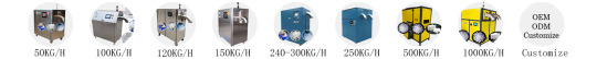
TECHNICAL SPECIFICATIONS
1. Size and portability:
Consider the physical size of the machine. A compact, portable unit may be better for versatility and ease of use, especially if you work from different locations or have limited space. If you need to move your cleaning equipment between job sites, choosing a dry ice blaster that is compact and portable may be key. This is important for tasks that require frequent movement or operation in limited spaces.
* Machine size: View the actual dimensions of your dry ice blaster, including length, width, and height. Make sure the machine is sized to fit your workplace and can be easily stored or carried.
* Weight: In addition to size, consider the weight of your dry ice blaster. The lightweight design can improve portability, reduce the burden of transportation, and make the device easier to carry and operate.
* Easy to carry design: Choose a machine with a user-friendly carrying design, such as handles, wheels, or other structures for easy movement. These designs make it easier for operators to move equipment from one location to another.
* Versatility: Some portable dry ice blasters are designed for versatility and can be used in a variety of applications. This flexibility increases the equipment's usefulness and makes it suitable for different types of cleaning tasks.
* Easy to store: Consider the storage needs of the machine when not in use. Some machines may have folding or removable parts to make it easier to store in limited spaces.
* Power and energy requirements: Consider the power and energy requirements of your dry ice blaster. Portable devices are often easier to connect to different types of power sources, such as batteries, generators, or standard electrical outlets.
When selecting a dry ice blaster, considering size and portability can ensure the equipment is better suited to your job requirements, increasing operational flexibility and efficiency.
2. Automation and control:
Automation and control are crucial considerations when selecting a dry ice pelletizer and cleaning machine. Look for user-friendly controls and automation features. An intuitive interface and automation streamline operation, making the machine easier for operators of all skill levels to use.
* Intuitive interface: Choose a dry ice granulator/cleaner with an intuitive interface. An intuitive control panel or touch screen makes it easier for operators to understand and operate the equipment, reducing training time.
* User-friendly controls: Consider choosing a machine with user-friendly controls. Simple buttons, knobs or digital controls allow operators to easily adjust and monitor cleaning parameters.
* Default program: Look for machines with preset cleaning programs. Preset programs improve operational consistency and efficiency, reducing manual setup and adjustments by the operator.
* Automation features: Understand whether the machine has automated functions, such as automatic nozzle adjustment, cleaning trajectory planning, etc. These features simplify the cleaning process and reduce operator intervention.
* Remote control and monitoring: If possible, choose machines that support remote control and monitoring. In this way, operators can monitor and adjust the cleaning process remotely, increasing the operational flexibility of the equipment.
* Fault diagnosis and alarm system: Look for machines with fault diagnosis and alarm systems. These systems can detect and report potential problems in a timely manner, helping to quickly resolve faults and improve equipment reliability.
* Data logging and reporting: Some advanced dry ice cleaning machines have data logging and reporting capabilities that can record key parameters during the cleaning process. This is very useful for quality control and traceability.
* Programmability: If you need to personalize it for a specific application, consider choosing a machine with some programmability to accommodate different cleaning needs.
By choosing a dry ice pelletizer/cleaner with an intuitive interface, automated features, and user-friendly controls, you can increase the ease of use of your equipment, reduce training costs, and ensure consistent cleaning results among operators of different skill levels .
Choosing the perfect dry ice machine requires a thorough understanding of your specific needs, technical specifications, and cost considerations. By carefully evaluating these factors, you will be able to make an informed decision that meets your application requirements and provides long-term value.
Whether you're venturing into a new business or upgrading an existing setup, investing the time in selecting the right dry ice machine is a critical step toward efficiency and success.
If you want to know more about Dry Ice Pellet Manufacturing Machinery or you want to build a dry ice production line, please refer to [Dry Ice Production Demystified: Go Behind the Scenes and Uncover the Magic of Pelletizers].
In this era of cleaning revolution, choose a dry ice cleaning machine to make cleaning easier, more efficient and more environmentally friendly! Thank you for reading our blog, if you have any questions or cooperation intentions, please feel free to contact us. Let us help the cleaning industry together and create a better future!
2 notes
·
View notes
Link
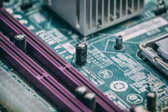
Get the best SMT and SMD Reflow Services in Gandhinagar and Ahmedabad, India. Our experienced team delivers fast, efficient, and high-quality results. Contact us now to get started!
Our services play a crucial role in the production of process control instruments for industrial and commercial applications, such as temperature, pressure, and flow control solutions.
#smd reflow#surface mountain device#smt#electronics manufacturing service#pcb contract manufacturing#pcb assembly#pcb soldering#pcb wave-soldering in ahmedabad#gandhinagar#ahmedabad#electronics industry#electronics in gandhinagar
0 notes