#pcb prototyping
Explore tagged Tumblr posts
Visit Tumblr Blog
Explore Tumblr blogs with no restrictions, modern design and the best experience.
Last Seen Tumblr Blogs


Fun Fact
Premium Tumblr themes are available from anywhere between $9 to $49.
Text
Understanding PCB Assembly

From prototyping to production, the complex process of building a printed circuit board (PCB), is crucial for ensuring functionality and reliability. Prototyping tests the PCB's functionality and identifies design issues, allowing engineers to refine and enhance the design. Advantages of thorough PCB assembly include early problem detection, comprehensive functional testing, cost efficiency, and the ability to make necessary design adjustments. Choose the right PCB assembly service to ensure successful, market ready products.
0 notes
Text
A4988 breakout prototype testing ⚙️🔧
We got our Allegro A4988 stepper driver breakout PCBs back and are ready to test them. First, we verified that STEP and DIR worked (yes!) and that the LEDs lit (yes, but we need to tweak the resistors to make the brightness even). Then we tried all of the stepper-settings, you can select 1, 4, 8, or 16-microsteps. All the sleep/reset/enable pins work. Finally, we checked the current limiting functionality with a potentiometer that can be twisted to select up to 2A current per coil. This directly affects the torque, so it's easy to test by verifying that we can stall the motor with hands or vise-grips. We'll order these with 2oz copper and get them into production next!
#a4988#stepperdriver#electronics#pcb#prototype#testing#breakoutboard#motorcontrol#microstepping#steppermotor#circuitdesign#electronicsengineering#makers#diyelectronics#hardware#engineering#currentlimiting#soldering#tinkering#pcblayout
42 notes
·
View notes
Text

#pcb#pcba#pcbassembly#pcb manufacturer#pcb board#pcb factory#pcb fabrication#aluminum pcb#pcb design#pcb prototype
2 notes
·
View notes
Text
PCB Manufacturing in Toronto: Expertise, Services, and Local Industry Insights
Discover PCB manufacturing in Toronto, a hub of innovation and quality in electronic manufacturing services. Learn about the specialized capabilities, technological advancements, and diverse offerings of PCB manufacturers Toronto. Explore how local expertise and cutting-edge facilities contribute to producing high-quality printed circuit boards for various industries and applications worldwide. For more details visit our website www.crimpcircuits.com
#pcb manufacturing toronto#printed circuit board design#metal clad pcb#printed circuits#rigid flex pcb#full turnkey pcb services#turnkey pcb services#pcb parts#eagle software#pcb designing#flexible pcb#pcb assembly#printed circuit board manufacturers#pcb manufacturers in canada#circuit board manufacturers in canada#pcb quote#pcb prototype services in canada
2 notes
·
View notes
Text

We are a 20 years PCB&PCBA factory.
4 notes
·
View notes
Text
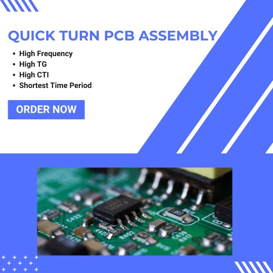
Quick-turn PCB assembly refers to an assembly service that can manufacture and assemble printed circuit boards in a very short turnaround time, generally taking only 24 to 48 hours to complete. Choosing a reliable quick turn PCB assembler matters, which provides you with high-quality circuit boards within the shortest time. But it’s not easy to make the correct decision as there are many quick-turn PCB assemblers available in the market.
Here are some points to help you choose the best quick turn PCB assembly service.
Experience
Speed
Quality
Equipment
Costs
Know more at: https://aaloktronix.com/what-is-quick-turn-pcb-assembly-know-about-its-fabrication-and-manufacturers/
2 notes
·
View notes
Text
Ever had misaligned components or assembly issues ruin your PCB production run? The culprit might surprise you!

Understanding PCB Fiducials:
In the fast-paced world of electronics manufacturing, precision is everything. Even the smallest details can influence the quality and reliability of the final product. One such crucial detail in PCB (Printed Circuit Board) design is the implementation of fiducials.
These tiny but powerful markers serve as alignment guides for automated assembly machines, ensuring accurate placement of components and flawless assembly. Despite their size, fiducials play a significant role in bridging design intent with manufacturing precision.
In this post, we'll explore PCB fiducials, why they matter, and how you can use them effectively in your designs.
What Are PCB Fiducials?
A fiducial mark, also known as a fiducial or registration mark, is a visual reference point on a Printed Circuit Board (PCB) that ensures precise alignment during manufacturing. These marks are essential for tasks such as aligning PCB layers, positioning stencils for solder paste application, and enabling accurate component placement by Pick-and-Place machines.
Typically, fiducials are simple geometric shapes, such as circles, etched or placed onto the bare PCB. They are made from copper and protected with an anti-oxidation coating to maintain their integrity. Fiducial locations are included in both the stencil design and Pick-and-Place data files.
During PCB assembly, automated machines use these reference points to confirm the correct positioning of the board. Fiducials also serve as measurable markers, acting as a reliable frame of reference for precise Surface Mount Technology (SMT) component placement.
Fiducials play a crucial role in maintaining accuracy across various assembly stages, serving multiple essential functions.
Purposes of PCB Fiducials:
Precise alignment and testing for automated optical inspection (AOI).
Accurately align PCB layers during fabrication.
Position components precisely during pick-and-place machine assembly.
Facilitate X-ray inspection for enhanced quality control.
Assist with precise alignment for board repair and rework.
Types of PCB Fiducials
There are three types of fiducial marks commonly found in PCB designs:
Global Fiducials: These are used to align the entire PCB. Typically, you'll find three global fiducials on a board, placed in a triangular arrangement to help machines recognize the board's orientation and position.
Local Fiducials: These are placed near specific components, especially fine-pitch components like BGAs (Ball Grid Arrays) or QFNs (Quad Flat No-leads). Local fiducials help in aligning the pick-and-place machine more accurately for these critical components.
Panel Fiducials: When multiple PCBs are manufactured on a single panel, panel fiducials are used to align the entire panel. This is common in mass production where multiple boards are processed simultaneously.

Placement and Design Considerations
The effectiveness of fiducials depends heavily on their placement and design. Here are some key considerations:
Location: Fiducials should be placed symmetrically across the PCB, ideally near the corners but away from the edges to avoid distortion during the fabrication process. This symmetry helps in accurate alignment.

The optimal size and shape of fiducials
Fiducials have a diameter of 1 mm,
Fiducials lie flat and are free of solder mask,
Fiducials are exposed in the solder mask 3 mm in diameter or square 3x3 mm.
If space is limited, it is also possible to place smaller fiducials. However, under no circumstances, they should be smaller than 0,5 mm. Moreover, they should have enough contrast by being surrounded by open areas.
Examples
OPTIMAL
OPTIONAL
MINIMAL
Diameter Fiducial Mark “d”
1 mm
1 mm
0.5 mm
Diameter of open area “2d”
1 mm
0.5 mm
0.25 mm
Diameter (Fiducial including open area)
3 mm
2 mm
1 mm

Two common PCB fiducial size and solder mask opening recommendations.
The typical size of a fiducial is around 1mm in diameter, though this can vary depending on specific design needs. The shape is usually circular to maintain consistency and ensure easy recognition by automated assembly machines.
Local fiducials generally measure around 1mm, with a solder mask opening of 2mm. However, it's crucial to account for the D-3D rule (as shown in the accompanying image), as manufacturers might prefer a larger solder mask opening for the fiducial based on its size. In most cases, local fiducials are kept to approximately 1 mm to help with trace routing and leave space for other components.
For very small components, such as 0201 resistors or tiny BGAs (Ball Grid Arrays), a local fiducial may not be necessary. In some situations, the fiducial could end up being larger than the component, making it redundant in the PCB layout. Therefore, it’s important to assess fiducial size carefully to ensure that it doesn't interfere with the overall design and component placement.
Clearance: It's important to maintain a clear area around each fiducial, free from traces, pads, or components. A common guideline is to have a clearance of at least 2 mm around the fiducial to avoid interference.
Solder Mask: Covering the fiducials with a solder mask can help prevent oxidation, ensuring that the fiducials remain clear and easy to detect throughout the assembly process.
Positioning of fiducials
Global and Panel Fiducials
Three fiducials per single PCB are arranged in “L”.
- For a multiple circuit board in a panel, three additional fiducials are arranged in “L” on the panel edge.
All fiducials are arranged as far on the outside as possible to create maximum distances. However, at least 5 mm to the edge (transport edge!) is needed.
Recommended reference designation: FD1, FD2 & FD3 for the TOP side, FD4, FD5 & FD6 for the BOTTOM side (these should be indicated as components in the Pick & Place file).
Fiducials should also be indicated in the solder paste data. (these are listed below during the production of the stencil).
Local fiducials
We recommend using local fiducials for components with a pin distance (pitch) ≤ 0,5 mm.
Three fiducials for each corresponding component should be arranged (minimum two diagonally),
Coordinates should be indicated in the same way as components (reference FDx-IC#) in the Pick & Place file,
Enough distance to the next component should be ensured (fiducials should still be visible after the assembly).
Best Practices for Using PCB Fiducials To maximize the effectiveness of your PCB fiducials, consider the following best practices:
Consistency: Use consistent fiducial designs across all your PCBs to streamline the assembly process. This consistency reduces the chance of errors during manufacturing.
Multiple Fiducials: Using three global fiducials is a common practice to provide a robust reference for alignment. This allows for better compensation for any potential skewing during the process.
Testing and Inspection: Always include fiducial placement as part of your design review process. Verifying their placement can prevent costly errors during manufacturing.
Common Challenges and How to Overcome Them While fiducials are crucial for accurate PCB assembly, there are challenges that designers must be aware of:
Misalignment Issues: Misalignment during the pick-and-place process can lead to faulty connections and component damage. Proper fiducial placement helps mitigate this risk by ensuring that machines can align the board correctly.
Manufacturing Tolerances: Variations in the PCB fabrication process can cause slight shifts in the board's dimensions. Fiducials help accommodate these tolerances, allowing the assembly machines to adjust for any minor discrepancies.
Conclusion
PCB fiducials may be small, but their impact on the manufacturing process is significant. By providing a reliable reference point for automated machines, fiducials ensure that your PCBs are assembled with precision and accuracy. As a designer or manufacturer, incorporating fiducials into your designs is not just a best practice—it's a necessity for delivering high-quality, reliable electronic products.
“Whether you're new to PCB design or a seasoned professional, understanding and using fiducials correctly will help you achieve better results and avoid costly errors in the assembly process”.
Fiducial Checklist Before Releasing for Production
Have you placed at least three fiducials on the PCB for global alignment?
Are the fiducials placed in non-linear positions to prevent misalignment?
For local fiducials, are they positioned close to critical components that require precise placement (e.g., BGAs or QFNs)?
Are the fiducials positioned away from high-density components or vias to avoid interference during placement?
Are the fiducials placed on both sides of the PCB (if required for double-sided assemblies)?
Are the fiducials placed on every board in case of a panel?
Are the panel fiducials 5 mm away from the edges?
Have you communicated the fiducial design and placement specifications with the manufacturer to ensure compatibility with their assembly machines?
Are the fiducials documented in the design files and included in the Pick-and-Place and Stencil files for production?
Reference
For Further information or if you are need to know more, Just click the link Auckam Technologies for expert support.
You can also visit or contact us through Linkedin, Instagram, Twitter, or Facebook.
#firmware#healthcare#drone#prototyping#prototype#hardware#pcb manufacturer#pcb assembly#pcb fabrication
0 notes
Text
We will explore how PCB prototypes shape the future of wearable devices and the impact they have on their design and functionality. For more information: https://www.pcb-togo.com/product/
0 notes
Text
In today’s fast-paced tech-driven world, companies need reliable partners who can deliver innovative solutions with speed and precision.
0 notes
Text
What is the Role of Proto PCBs in Developing Cutting-Edge Rigid Flex Circuit Boards?
In the energetic world of gadgets, the request for compact, flexible, and solid arrangements is continually developing. One development tending to these needs is Rigid Flex Circuit Boards. These cross breed circuit Boards combine Rigid and flexible substrates to offer improved usefulness, plan flexibility, and solidness. In any case, their improvement is complicated, requiring cautious plan, prototyping, and testing. This is where Proto PCBs play an crucial part. They act as foundational instruments in the travel from concept to last item. This article dives into how PCB Prototypes contribute to the advancement of cutting-edge Rigid Flex Circuit Boards.
Understanding Rigid Flex Circuit Boards
Rigid Flex Circuit Boards are a consistent mix of Rigid and flexible circuit layers interconnected to make a single structure. This interesting plan permits engineers to coordinated flexible areas that twist and adjust to complex shapes whereas keeping up Rigid areas for components requiring steadiness. Businesses such as aviation, restorative, car, and customer gadgets depend intensely on Rigid Flex Circuit Boards for their compact estimate, lightweight plan, and upgraded unwavering quality in challenging environments.
Despite their points of interest, creating Rigid Flex Circuit Boards includes complicated designing challenges, especially in guaranteeing mechanical steadiness, flag keenness, and manufacturability. These complexities request thorough testing, which is where Proto PCBs are pivotal.

What are Proto PCBs?
A Proto PCB (Prototype Printed Circuit Board) is a preparatory adaptation of a PCB outlined to test and approve a circuit’s usefulness. Proto PCBs permit engineers to try with plans, distinguish imperfections, and refine them some time recently continuing to full-scale generation. For Rigid Flex Circuit Boards, Proto PCBs offer assistance approve basic viewpoints like adaptability, flag execution, warm administration, and component integration.
Role of Proto PCBs in Creating Rigid Flex Circuit Boards
1. Testing and Approval of Design
Rigid Flex Circuit Boards include complex formats where Rigid and flexible layers are interlaced. A PCB prototype permits engineers to test the starting plan beneath real-world conditions. Engineers can assess the execution of interconnects, guarantee that the flexible parts can withstand rehashed twisting, and recognize potential powerless focuses. Proto PCBs moderate dangers of disappointment by uncovering issues early in the plan process.
2. Optimization of Fabric Selection
The choice of materials is basic for Rigid Flex Circuit Boards as it influences solidness, adaptability, and warm execution. Proto PCBs empower engineers to test different substrate combinations and cement definitions to decide the best fit for their application. This step is fundamental for guaranteeing that the board meets the execution and unwavering quality criteria required in businesses like aviation or therapeutic devices.
3. Cost-Effective Iterations
Prototyping is a cost-effective way to refine a plan. Without the utilize of Proto PCBs, creating a cutting-edge Rigid Flex Circuit Board may result in exorbitant mistakes amid mass generation. Emphasizing with Proto PCBs guarantees each consequent plan progresses in usefulness and manufacturability, decreasing the chance of costly rework.
4. Assessment of Adaptability and Durability
Proto PCBs play a basic part in testing the energetic angles of Rigid Flex Circuit Boards. Flex cycles, stress tests, and thermal simulations are performed utilizing these Prototypes to guarantee the board withstands the mechanical and natural requests of its application. Engineers can recognize plan blemishes, such as delamination or stretch breaks, some time recently last production.
5. Signal Astuteness and Execution Analysis
The blended design of Rigid Flex Circuit Boards postures one of a kind challenges in keeping up flag astuteness. Proto PCBs empower point by point investigation of flag execution, control dispersion, and commotion impedances in the plan. By tending to these issues amid prototyping, the last item conveys ideal performance.
6. Alignment with Fabricating Requirements
Manufacturing complex Rigid Flex Circuit Boards includes forms like cover, penetrating, and patching that must be exact. Proto PCBs are utilized to confirm manufacturability and distinguish potential generation bottlenecks. Plan groups collaborate with fabricating accomplices utilizing these Prototypes to streamline generation workflows and diminish waste.
Conclusion
In the fast-paced world of innovation, development and unwavering quality are vital, particularly in gadgets that depend on Rigid Flex Circuit Boards. Proto PCBs act as the bridge between conceptual plan and wrapped up item, permitting engineers to refine their thoughts through iterative testing and optimization. By tending to potential imperfections, moving forward fabric determination, and guaranteeing manufacturability, Proto PCBs clear the way for cutting-edge PCB Prototypes to change into high-performance Rigid Flex Circuit Boards. Their part is vital in turning driven plans into unmistakable, market-ready items that drive advance in advanced gadgets.
0 notes
Text
In today’s fast-paced electronics industry, quick and accurate PCB production is critical for staying competitive.
0 notes
Text
The first test for our WLED board codename "Sparkle Motion" 🌈💖💡 … 🐇⏳🌌
We got our WLED-friend PCBs today, and we only made one mistake: the wrong resistor on the 3.3V feedback line. Now that it's fixed, the board seems to work great with the latest version of WLED
We are checking all 4 signal outputs with this handy 256-LED grid that sits on our desk. Next, we will test the onboard IR receiver, USB PD, I2S microphone, extra I/O pins, and I2C. We'll also do an Arduino IDE board definition in case folks want to use it as a generic ESP32-to-LED-driver board. We're calling the board "Sparkle Motion" for now, but if you have other naming ideas, let us know - if we pick your name, you get a free board
Sign up, coming soon.
#wled#sparklemotion#leddriver#esp32#electronics#pcbs#arduino#makerprojects#openhardware#opensource#coding#leds#hardwaredesign#innovation#techgeeks#smartlighting#microcontrollers#hardwareengineering#esp32projects#ledmatrix#diyhardware#iotprojects#arduinoide#hardwaretesting#ledtechnology#techmakers#electronicscommunity#prototyping#hardwarehacking#adventuresintech
16 notes
·
View notes
Text

#pcb#pcba#pcbassembly#aluminum pcb#pcb design#pcb fabrication#pcb factory#pcb manufacturer#pcb board#pcb prototype
2 notes
·
View notes
Text
Common Mistakes in Prototype Circuit Board Design And the Way to Avoid Them
Embarking on the journey of prototype circuit board design is an exciting yet challenging endeavor. In the rapidly evolving world of electronics, staying ahead requires vigilance against common mistakes that could jeopardize your project's success. In this article, we will explore these pitfalls and provide valuable insights on how to avoid them. As a leading provider of PCB fabrication and assembly services, HitechCircuits offers expertise and state-of-the-art capabilities to ensure your prototype circuit board designs are flawless.
Common Mistakes in Prototype Circuit Board Design:
Inadequate Planning:
One of the most common mistakes is rushing into the design phase without thorough planning. Skipping the crucial step of defining your project's requirements and specifications can lead to design flaws and performance issues. To avoid this, take the time to create a detailed plan outlining your objectives, components, and functionality.
Ignoring Design Rules:
Every PCB manufacturer has specific design rules and guidelines. Neglecting these rules can result in manufacturing difficulties and compromised board functionality. Hitech provides comprehensive design guidelines to ensure your prototype circuit board aligns seamlessly with their manufacturing processes, minimizing the risk of errors.
Common PCB prototyping rules that have to be followed:
· Component Placement
· Trace Routing
· Layer Stack up
· Clearances and Spacing
· Via Placement
· Trace Width and Spacing
· Decoupling Capacitors
· Grounding Strategy
· Thermal Management
· Design for Manufacturability (DFM)
· Testability and Debugging
· Documentation
Component Placement and Routing Issues:
Poor component placement and routing decisions can lead to signal integrity problems and increased interference. Carefully consider the arrangement of components on your prototype circuit board and optimize the routing to minimize signal crosstalk and electromagnetic interference.
Insufficient Power Distribution:
Inadequate power distribution can result in voltage drops and uneven power delivery, impacting the overall performance of your circuit. Properly distribute power planes and use suitable decoupling capacitors to ensure stable and reliable power distribution across your prototype circuit board.
Insufficient power distribution in PCB design can give rise to several issues, negatively impacting electronic devices and systems. The problems associated with inadequate power distribution include unwanted voltage drops, insufficient power supply to components, and a decline in overall performance.
Here are the key concerns linked to improper power distribution:
· Voltage drop
· Decoupling capacitors connected improperly
· Grounding issues
Inadequate Testing Protocols:
Neglecting testing during the design phase can be a costly mistake. Implement thorough testing protocols to identify and rectify potential issues early in the development process. Utilize Hitech's advanced testing capabilities to ensure the reliability and functionality of your prototype circuit board.
Insufficiency in Signal Integrity
Overlooking signal integrity in PCB design can lead to complications like noise, reflections, and signal distortions, significantly affecting the overall performance of the circuit. Inadequate attention to signal integrity may give rise to problems such as reflections, cross-talk, signal loss, power transmission issues, and challenges with high-frequency transmission.
· Reflections
· Cross Talk
· Signal Loss
· Power transmission
· High-frequency Transmission
To address these concerns proactively, it becomes crucial to employ simulation tools, incorporate optimal techniques and practices, and consistently test signal integrity throughout the PCB design process.
Avoiding Common Mistakes in Prototype Circuit Board Design:
· Plan the layout carefully
· Follow design guidelines
· Use appropriate materials
· Double-check component footprints
· Pay attention to trace routing
· Test critical connections
· Include test points
· Document the design thoroughly
· Minimize vias and use them strategically
· Ensure proper clearances
· Prototype in small batches
· Collaborate with Experienced Engineers
· Efficient Power Distribution
Summary:
Mastering prototype circuit board design requires a combination of careful planning, adherence to best practices, and collaboration with experienced professionals, etc. By avoiding common mistakes and leveraging the expertise of reliable partners like HitechCircuits, you can ensure the success of your electronic projects. Invest time in meticulous planning, embrace advanced design tools, and take advantage of the cutting-edge capabilities offered by PCBGOGO to bring your prototype circuit board designs to life with precision and excellence.
0 notes
Text
Factors to Consider When Selecting A Low-Cost PCB Manufacturer
Choosing the right low-cost PCB manufacturer can be challenging, especially with many available options. To help you make an informed decision, we've outlined five key factors to consider when selecting a low-cost PCB manufacturer.

#custom pcb manufacturing#pcb fabrication#pcb manufacturer in india#prototype pcb manufacturing#pcb manufacturer#two layer pcb stencil#pcbcircuit#best pcb stencil maker in hyderabad#pcb manufacturer in delhi#pcb manufacturer in maharashtra
0 notes
Text
Top PCB Manufacturer in India
PCBcircuit is a leading PCB manufacturer in India, offering high-quality printed circuit boards tailored to diverse industries. With advanced technology, precision engineering, and reliable customer support, we ensure efficient and cost-effective PCB solutions to power your innovations. Trust PCBcircuit for quality and excellence in PCB manufacturing.

#flex pcb manufacturer#prototype pcb manufacturing#pcb manufacturer#custom pcb manufacturing#low-cost pcb manufacturer#pcb fabrication#quick turn pcb fabrication#high-quality pcb manufacturing#multilayer pcb manufacturer
0 notes