#VLSI Projects
Explore tagged Tumblr posts
Visit Tumblr Blog
Explore Tumblr blogs with no restrictions, modern design and the best experience.
Last Seen Tumblr Blogs


Fun Fact
Tumblr is used by 21% of adults online aged 18-29 years.
Text
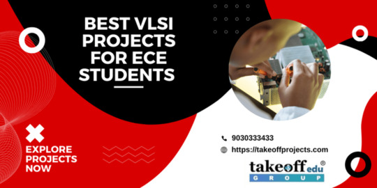
Best VLSI Projects for ECE Students
Very Large Scale Integration (VLSI) is a crucial domain in Electronics and Communication Engineering (ECE), offering opportunities to design and develop microchips and complex electronic circuits. Here are some of the best VLSI project ideas for ECE students that can enhance their knowledge and career prospects:

FPGA-Based System Design: Field-Programmable Gate Arrays (FPGAs) are widely used in the industry for prototyping. Students can design a system using FPGA for applications such as real-time video processing, digital signal processing, or cryptography.
Low-Power VLSI Design: With the growing demand for energy-efficient devices, low-power VLSI design projects like creating low-power adders, multipliers, or memory circuits can be impactful and highly relevant.
ASIC Design for IoT Applications: Application-Specific Integrated Circuits (ASICs) are tailored for specific purposes. Designing ASICs for IoT devices, such as smart sensors or wearable technology, is a cutting-edge project idea.
Digital Signal Processing (DSP) Architecture: DSP is critical for applications like audio processing, image processing, and telecommunications. Implementing DSP algorithms on VLSI platforms offers practical insights.
High-Speed Processor Design: Designing processors with high-speed operation and reduced latency is a challenging yet rewarding project. Focus on architectures like RISC or multi-core processors.
Memory Design and Optimization: Projects focusing on memory units such as SRAM, DRAM, or Flash memory can help students understand memory hierarchy, speed, and power trade-offs.
Verification and Testing of VLSI Circuits: Verification ensures the accuracy of designs before fabrication. Projects in this area can include creating automated verification environments using tools like Verilog or SystemVerilog.
By undertaking these projects, students not only gain technical expertise but also develop problem-solving and analytical skills, preparing them for a thriving career in the VLSI industry.
#VLSI Projects#Engineering Projects#Final Year Projects#VLSI Final Year Projects#Btech Projects Major Projects#VLSI Major Projects
0 notes
Text
Exciting Electronic projects for your Academic Projects
At Takeoff Edu Group, we merge creativity with skill to work electronic wonders. Here, we are passionate to helping everyone get into cool Electronic projects. Whether you're really good at engineering or just starting to learn, we have plenty of stuff to help you out and keep your ideas coming. We've got something for everyone, whether you like making your own gadgets or working on fancy robots. Our community is full of people who love creating things. Come with us as we explore, try things out, and come up with cool ideas in the fun world of electronic projects.

Here are the Takeoff Edu group titles for Electronic projects:
Latest:
High-Precision and Low-Power Offset Cancelling Tri-State Sensing Latch in NAND Flash Memory
Trendy:
Performance Analysis of 4-Bit Multiplier using 90nm Technology
An Accurate Low-Power Power-on-Reset Circuit in 55-nm CMOS Technology
Low Power and High-Performance Associative Memory Design
Low Power, High Performance PMOS Biased Sense Amplifier
Low-Power Retentive True Single-Phase-Clocked Flip-Flop With Redundant-Recharge-Free Operation
Design and Analysis of Low-Power High Performance 4-Bit Parallel Shift Register using Retentive True Single Phase Clocked D-Flip Flop
Standard:
Optimizing Ternary Multiplier Design with Fast Ternary Adder
High Efficient GDI-CNTFET-Based Approximate Full Adder for Next-Generation of Computer Architectures
Design and Implementation of a Low Power Ternary Content Addressable Memory (TCAM)
Accounting for Meritor I-V Non-linearity in Low Power Memristive Amplifiers
Optimizing Ternary Multiplier Design with Fast Ternary Adder
The Above Electronic project are the example titles of Takeoff Edu Group. Here we not only provide Electronic projects, but also furnishes all kind of project to upgrade your skills and improve your innovation levels for Students as well as hobbyists. Takeoff Edu Group gives you a proper guidance and support to those peoples who are eager to learn more about these projects with step-by-step instructions and detailed explanations.
0 notes
Text
Best final year engineering projects

Welcome to our webpage dedicated to engineering projects! We are a team of experienced engineers and developers who specialize in creating innovative and cutting-edge projects for students and professionals.
Our goal is to provide individuals with the opportunity to showcase their skills and knowledge while working on real-world engineering projects that have the potential to make a positive impact on society. Our projects are designed to help individuals develop their technical and professional skills and to prepare them for successful careers in their chosen fields.
Reversible Logic-Based 1-bit Comparator using QCA
Heat and energy dissipation are the immense problems in today's processor design. These problems can be overcome if reversible logic is used for the design implementation. In this paper, the 1-bit comparator based on reversible logic is proposed. Further, the reversible logic gates used in the proposed design are implemented using "Quantum-dot Cellular Automata (QCA) nanotechnology". QCA is a viable technology among various nanotechnology through which reversible logic can be implemented at the device level with low energy, less area and high speed. The simulation is backed by the QCA Designer tool. The proposed design is single-layered which is also optimized for area, energy and delay.
Efficient Design of Vedic Square Calculator Using Quantum Dot Cellular Automata QCA
Vedic mathematics is now being realized to have a large potential in recent times which can be used to design digital circuits using the Vedic formulas. Vedic mathematics is a new trend in quantum-dot cellular automata (QCA) technology. However, an efficient coplanar design and a complete performance analysis are still desired. This brief presents the coplanar QCA architecture of a 2-bit square calculator (proposed design-1 or PD1) using the Vedic sutra 'Urdhva Tiryagbhyam'. Furthermore, based on the E-shaped XOR gate and majority gate (MV) an optimized architecture (proposed design-2 or PD2) is presented. The PD2 architecture exhibits notable improvement compared to the previous architecture. It is worth mentioning that the comprehensive performance analyses are carried out using the QCADESINER.
A Cost-Efficient QCA XOR-XNOR Topology for Nanotechnology Applications
A quantum-dot cellular automaton (QCA) is an inventive Nano-level computation that suggests fewer dimensions, and less power consumption, with more speed and premeditated as an amplification of the scaling obstacle. with the CMOS methodology. One of the newest and rising nanotechnologies used today is QCA based on the repulsion of Coulomb. One of the newest and rising nanotechnologies is The QCA based on the repulsion of Coulomb is used today. Surmised computing is a successful paradigm for energy-efficient hardware design at the Nano-scale. In this project, We proposed a proficient, low-complex 2-bit & 3-bit XOR, XNOR, 2-bit An XOR/NOR gate has been suggested in QCA technology. Next, using those proposed A 4:2 encoder and a 4:1 encoder are designed in QCA technology.
Area Efficient Multilayer Arithmetic Logic Unit Implementation in Quantum-dot Cellular Automata
Quantum-dot Cellular Automata (QCA) is a new nano-scale technology that due to making significant improvements in the design of electronic circuits can be considered as an appropriate alternative to CMOS technology. The Arithmetic Logic Unit (ALU) is a fundamental component of the Central Processing Unit (CPU) to carry out the arithmetic and logical operations the multiplexer and full adder plays an important role in its operations. In this paper, a QCA multiplexer is proposed based on the cell interaction with less number of cell count. Likewise, a QCA multilayer ALU structure is designed to perform both arithmetic and logical operations.
Binary Coded Decimal Seven Segment Circuit Designing using Quantum-dot Cellular Automata
Quantum-dot Cellular Automata (QCA) is new due to making significant improvements in the design of electronic circuits can be considered as an appropriate alternative to CMOS. technology. It is an alternative nanotechnology that keeps scaling down. The technology is further It can do scaling beyond to a level where complementary Metal oxide semiconductor (CMOS) scaling is the issue. QCA is seen as an emerging solution for nano-architectures.
Conclusion: Engineering projects play a pivotal role in addressing societal needs and driving progress. By harnessing technology, innovation, and sustainable practices, these projects offer solutions to complex problems. From enhancing urban infrastructure to revolutionizing healthcare and space exploration, they exemplify the transformative potential of engineering. As we continue to invest in these endeavors, we move closer to a more sustainable, efficient, and interconnected world. More Info
0 notes
Text
https://youtu.be/Af2jPMwhpY0?si=EWzkeRfAbNUiuIhS
1 note
·
View note
Text
Vlsi projects
VLSI (Very Large Scale Integrated) projects are an important part of the ece curriculum. The use of VLSI technology allows students to learn about and apply advanced calculus and engineering principles to real-world problems. This technology is also a great way for students to develop problem-solving skills and apply them in a business setting.
0 notes
Text
Unveiling VLSI Technology: Navigating Complexity for a Transformed Tomorrow
Discover the intricate world of VLSI technology in our latest article. Delve into the fundamental concepts and applications that drive the VLSI industry forward. Explore the transformative impact of VLSI in modern electronics. Uncover the secrets behind designing complex integrated circuits. Learn how VLSI certification courses at Golden Barrel Technical Education can pave the way for a successful career in this cutting-edge field.
0 notes
Text
0 notes

Text
VLSI Training in Chennai : Master the Art of Chip Design and Fabrication. Introduction Welcome to our comprehensive guide on VLSI (Very Large-Scale Integration) training in Chennai, where we delve into the fascinating world of chip design and fabrication. In this article, we will explore the importance of VLSI in the field of electronics, the benefits of VLSI training, and how our training program can equip you with the skills and knowledge to excel in this high-demand industry. If you're passionate about cutting-edge technology and want to be at the forefront of chip design, read on!
The Significance of VLSI VLSI refers to the process of integrating thousands, or even millions, of transistors onto a single chip. This technology has revolutionised the field of electronics by enabling the development of smaller, faster, and more powerful integrated circuits. VLSI plays a vital role in various sectors, including consumer electronics, telecommunications, automotive, aerospace, and healthcare. From smartphones and computers to medical devices and self-driving cars, VLSI is the backbone of modern technology.
Why VLSI Training? VLSI design and fabrication require specialised skills and
knowledge. By undergoing VLSI training, you can gain a competitive edge and open up a world of opportunities. Here are some key reasons why VLSI training should be your next career move:1. High-Demand Industry The VLSI industry is thriving, with a constant demand for skilled professionals who can design and develop complex integrated circuits. By acquiring VLSI skills, you position yourself for a rewarding career with excellent growth potential. Companies across the globe are constantly seeking VLSI experts to drive innovation and develop cutting-edge electronic products.
2. Diverse Career Options VLSI offers a diverse range of career options. As a VLSI professional, you can work as a VLSI design engineer, verification engineer, physical design engineer, FPGA engineer, or system-on-chip (SoC) designer, among others. You can choose to work in semiconductor companies, research and development labs, or even start your own entrepreneurial venture in chip design.
3. Innovation and Advancement VLSI professionals have the opportunity to be at the forefront of technological advancements. By mastering VLSI, you become part of a dynamic field where innovation is key. You'll be involved in designing next-generation chips that power a wide range of applications, from artificial intelligence and machine learning to internet of things (IoT) devices and advanced communication systems.
4. Lucrative Salary Packages The specialised skills and expertise in VLSI command attractive salary packages. The demand for VLSI professionals is high, and companies are willing to offer competitive compensation to secure top talent. By investing in VLSI training, you can position yourself for a financially rewarding career in the semiconductor industry.
The Benefits of our VLSI Training Program in Chennai When it comes to VLSI training in Chennai, we are committed to providing a comprehensive learning experience that prepares you for success. Here's why our training program stands out:
1. Industry-Relevant Curriculum Our VLSI training program offers an industry-relevant curriculum designed to cover the fundamental concepts and advanced techniques of VLSI design and fabrication. You'll learn about digital design, analog and mixed-signal design, physical design, verification methodologies, and more. Our curriculum is regularly updated to align with the latest industry trends and technologies.
2. Hands-on Practical Experience We believe in learning by doing. Our VLSI training program provides hands-on practical experience through industry projects, lab sessions, and simulations. You'll work with industry-standard tools and software used in chip design and fabrication, gaining valuable experience and building a strong foundation in VLSI.
3. Expert Faculty and Mentors Our trainers and mentors are experienced VLSI professionals with a wealth of knowledge and industry expertise. They provide guidance, support, and mentorship throughout your training journey, ensuring you receive the best possible education and practical insights. You'll have the opportunity to learn from industry veterans and gain valuable insights into the VLSI industry.
4. Placement Assistance We are dedicated to your success beyond the training program. Our placement assistance program helps connect you with top VLSI companies and job opportunities in Chennai and beyond. We provide guidance on resume building, interview preparation, and job search strategies to increase your chances of landing your dream job in the VLSI industry.
Conclusion In conclusion, best VLSI training in Chennai opens up a world of opportunities in the fast-paced semiconductor industry. By mastering the art of chip design and fabrication, you'll be at the forefront of technological innovation and contribute to the development of cutting-edge electronic products. Don't miss out on the chance to acquire in-demand skills and embark on a rewarding career in VLSI.
ServicesNow Training in Chennai
Alteryx training in chennai
AWS Training in Chennai
Digital Marketing Course in Chennai
VLSI Training in Chennai
Catia Training in Chennai
Angular JS Training in Chennai
React training in Chennai
AWS Online Job Support From India
AWS Online Job Support From India
#vlsi projects#vlsitraining#traininginchennai#chennai#innovation#incorrect quotes#instagram#interiors#the#inspiration#spilled ink
0 notes
Text
Top 20 VLSI Projects for Final Year Students 2023
Discover top 20 VLSI projects showcasing cutting-edge innovations in integrated circuits for final year students and diverse applications.
0 notes
Text
Best VLSI Projects for ECE Students
The terminology “VLSI” means Very Large Scale Integration Technology. It is usually concerned with the development of integrated circuits by merging several thousands of transistor circuitries with numerous kinds of logical circuitries. Contrary to the conventional integrated circuits, the integrated circuits built using VLSI concepts consume less area and space for the sake of optimization.
Best Tools Used for VLSI Projects
As far as the VLSI designs are concerned, many different tools are being utilized depending on the applications served. Furthermore, several fabrication methodologies are being adopted. Let us now look at the best Tools used for VLSI projects:
Siemens EDA
Synopsys
Cadence EDA
Silvaco
Tanner EDA
Xilinx Vivado
Xilinx ISE
VLSI Project Genres
While pursuing the projects on VLSI, the students have the option to choose their diverse topics spanning from building of the fundamental digital circuitry to sophisticated circuitry. Some of those genres within VLSI are indicated below.
VLSI serving machine learning
Raised-speeded VLSI
Reduced-powered VLSI
Within the realm of VLSI Projects, there are certain exciting areas to do the final year projects. Some of those exciting areas, namely, System-on-a-Chip (SOCs); MATLAB; IEEE standards; Field Programmable Gate Array applications (FPGAs); Xilinx, etc. These projects can be undertaken by both UG and PG engineering course-pursuing students. We are now curating and presenting the students with such projects in the following bulletins:
Conclusion
The VLSI field has the potential to host a diverse range of projects for engineering students, which can help in providing sustainable solutions like reduced-power operating circuitry. VLSI Projects can also serve certain state-of-the-art applications like cryptography, image identification, and the Internet of Things (IoT).
#VLSI Projects#Engineering Projects#Final Year Projects#VLSI Final Year Projects#Btech Projects Major Projects#VLSI Major Projects
0 notes
Text
Unique Cadence EDA Projects for Engineering Students
Cadence EDA Project is the all-in-one EDA solution dedicated to EDA, which combines the tool and the solution in one powerful package that facilitates the creation of the integrated circuits (ICs) and electronic system. Starting with schematic and topographical design, we offer our integrated environment, enabling engineers to create designs that are very effective and precise by the standard of the engineering profession. Takeoff Edu Group Provide Unique projects for final year students.
With 3D CAD, in-circuit engineering, advanced modelling, and signal integrity analysis tools, the platform enables power optimization, design for manufacturability, and solving of complex design challenges to feature products with high performance and reliability. EDA provides the project designs either in analogy, digital or mixed-signal designs that equip the engineer to conceive the idea into the product while also meeting the industry requirements and ensuring reduced time to market.

Takeoff Edu Group-Example titles for Cadence EDA Project
Trendy:
Fixed-Posit: A Floating-Point Representation for Error-Resilient Applications
An Area Efficient 1024-point Low Power Radix-22 Fft Processor with Feed-forward Multiple Delay Commutators
Standard:
Vedic-Based Squaring Circuit Using Parallel Prefix Adders
An Analysis Of DCM-based True Random Number Generator
Static Delay Variation Models for Ripple-carry and Borrow-save Adders
A Two-speed, Radix-4, Serial–Parallel Multiplier
A Systematic Delay and Power Dominant Carry Save Adder Design
The most common projects in this regard are centered around the utilization of Cadence's extensive collection of software tools and platforms, which address different stages of the design cycle, from idea development to final product development alike. One puzzle of Cadence EDA projects that are solved is circuit design. Engineers utilize Virtuoso for schematic entry and layout creation, where they assure themselves that complex integrated circuits can be implemented efficiently. As well as Cadence's simulation and verification tools, Spectre and Incisive, these tools are vitally important in validating the functionality and performance, identifying the possible errors that might cause fabrication problems. Additionally, in their EDA projects, Cadence uses physical implementation tools such as Encounter to perform layout and timing optimizations, thus attaining high chip design robustness and reliability. In addition, the rapid emergence of high-tech semiconductor device manufacturers such as silicon photonically leads Cadence EDA projects to include mainly custom IC design, RFIC (Radio Frequency Integrated Circuit) design, and mixed-signal verification, which meet various market requirements. In the frame of collaborative work and innovative methods, progress in electronic design is achieved by Cadence EDA projects. The development of the most advanced hardware solutions that are put to use in multiple areas, such as consumer electronics and automotive, and many others beyond, is facilitated and promoted by such projects. Fundamentally, the Cadence EDA projects unite design expertise and technology with creativity to impact positively the changes in the developing semiconductor design realm.
The Cadence EDA Projects is one of the most important components in today's engineering by enabling Takeoff Projects to create and be more advances. During the team's project with Cadence software, we saw an increase in productivity and higher precision level in designing electronic circuits. From schematic capture to layout and verification, Cadence EDA proved very suitable for our workflow which was being to meet a timely delivery of high quality solutions. Leveraging our circuit simulation and optimization skills, we bravely took on complex issues with confidence. Further, this dedication to constant improvement maintains the development of our projects in the vanguard of technology. By and large, Cadence EDA Projects have been playing a key role in Takeoff Projects’ journey to keeping the projects afloat amidst the ever-evolving world of electronic design.
#VLSI Projects#Cadence EDA Projects#VLSI Cadence EDA Projects#Academic Projects#Final Year Projects#Engineering Projects
0 notes
Text
Design for Testability in VLSI: Enhancing Reliability and Efficiency:
The efficiency and dependability of integrated circuits are critical in the field of Very Large Scale Integration (VLSI). Using Design for Testability (DFT) techniques is a crucial step in reaching this goal. DFT focuses on adding features to the design process that make it simpler to test and identify possible flaws, which eventually improves overall performance and shortens time-to-market.
The Crucial Role of Design for Testability in VLSI
Analyse the Design for Testability (DFT)'s strategic importance in VLSI circuit testing. This section addresses the issues raised by the growing complexity of VLSI designs and explores why DFT is essential to guaranteeing the dependability and effectiveness of integrated circuits.
Important Design for Testability in VLSI Techniques:
To improve testability in VLSI, a number of DFT techniques are used. Using built-in self-test (BIST) structures is one popular technique that enables the chip to create and run test patterns on its own. Another popular method that makes testing easier is the use of scan chains, which allow test data to be loaded and unloaded serially. Boundary scan testing also makes sure that input and output pins are thoroughly inspected, which adds to a full assessment of the chip's functionality.
Effect on Cost and Time-to-Market:
Design for Testability speeds up the entire product development cycle by cutting down on the amount of time needed for testing and debugging.
Key DFT Techniques:
A number of DFT methods are used to improve VLSI testability. Using built-in self-test (BIST) structures is one popular technique that enables the chip to create and run test patterns on its own. Another popular method that makes testing easier is the use of scan chains, which allow test data to be loaded and unloaded serially. Boundary scan testing also makes sure that input and output pins are thoroughly inspected, which adds to a full assessment of the chip's functionality.
Additionally, a more testable design makes it possible to execute productive manufacturing procedures, which strengthens a company's position in the market
In conclusion,
It is critical to prioritize Design for Testability in the constantly changing field of VLSI design. Engineers can improve integrated circuits' cost-effectiveness, efficiency, and reliability during the design process, paving the way for their seamless integration into the quickly evolving world of electronic gadgets.
1 note
·
View note
Text
youtube
Use this trick to Save time : HDL Simulation through defining clock
Why is this trick useful? Defining a clock in your simulation can save you time during simulation because you don't have to manually generate the clock signal in your simulation environment. Wanted to know how to define and force clock to simulate your digital system. Normally define clock used to simulate system with clock input. But I am telling you this trick for giving values to input ports other than clock. It will help you to save time in simulation because you do not need to force values to input ports every time. Lets brief What we did - gave some clock frequency to input A, like we gave 100. Than we made Half the frequency of clock to 50 and gave it to Input B. In similar way if we have 3rd input too we goanna half the frequency again to 25 and would give to next input.
Subscribe to "Learn And Grow Community"
YouTube : https://www.youtube.com/@LearnAndGrowCommunity
LinkedIn Group : https://www.linkedin.com/groups/7478922/
Blog : https://LearnAndGrowCommunity.blogspot.com/
Facebook : https://www.facebook.com/JoinLearnAndGrowCommunity/
Twitter Handle : https://twitter.com/LNG_Community
DailyMotion : https://www.dailymotion.com/LearnAndGrowCommunity
Instagram Handle : https://www.instagram.com/LearnAndGrowCommunity/
Follow #LearnAndGrowCommunity
#HDL Design#Digital Design#Verilog#VHDL#FPGA#Digital Logic#Project#Simulation#Verification#Synthesis#B.Tech#Engineering#Tutorial#Embedded Systesm#VLSI#Chip Design#Training Courses#Software#Windows#Certification#Career#Hardware Design#Circuit Design#Programming#Electronics Design#ASIC#Xilinx#Altera#Engineering Projects#Engineering Training Program
2 notes
·
View notes
Text
Designing Energy-efficient Systems with VLSI Projects
With the increasing demand for energy, there is a need to optimize energy consumption in different applications. VLSI projects are one of the most important tools for designing energy-efficient systems. VLSI stands for “very large-scale integration” and is the process of creating a single integrated circuit on a chip. It involves packing millions of electronic components on a single semiconductor substrate. In the past, integrated circuits were created by combining many single-chip circuits. However, VLSI projects are a more efficient way to design integrated circuits, as the components are integrated on the same chip.
VLSI projects can be used to design systems that are more energy-efficient than traditional designs. By reducing the number of components, reducing the area of the circuit, and using low-power components, energy consumption can be reduced. The use of low-power components also reduces the amount of heat generated by the circuit. This makes it easier to cool the system, reducing energy consumption.
VLSI projects can also be used to reduce the power consumption of systems by optimizing the use of the circuits. By optimizing the circuits, the amount of power used can be reduced. This can reduce the overall energy consumption of the system.
In addition to reducing the energy consumption of a system, VLSI projects can also be used to increase the speed and performance of a system. By creating a more efficient system, the system can run faster and with better performance. This can result in improved system performance and reduced energy consumption.
VLSI projects are an important tool for designing energy-efficient systems. By reducing the number of components, reducing the area of the circuit, and using low-power components, energy consumption can be reduced. The use of low-power components also reduces the amount of heat generated by the circuit. In addition, VLSI projects can be used to optimize the use of circuits, resulting in improved system performance and reduced energy consumption.
0 notes
Text
https://goldenbarreledu.com/vlsi-design-and-varification-course-providers-in-bangalore/
Golden Barrel: Your Path to VLSI Excellence in Bangalore
Looking to master VLSI design and technology? Look no further than Golden Barrel, the premier VLSI training institute in Bangalore!
At Golden Barrel, we provide top-notch VLSI training that equips you with the knowledge and skills essential for a successful career in the semiconductor industry. Our expert instructors, industry-aligned curriculum, and state-of-the-art facilities make us the ideal choice for VLSI enthusiasts.
0 notes