#Semiconductor Fab
Explore tagged Tumblr posts
Visit Tumblr Blog
Explore Tumblr blogs with no restrictions, modern design and the best experience.
Last Seen Tumblr Blogs


Fun Fact
In 2020, Tumblr had 29.4 million users in the US.
Text
Hello everyone, and this is «Technology from USSR which everybody pretends is brand new»
Today's technology in the spotlight is: minifab, an incomplete version of which is known as "minimal fab".

3 notes
·
View notes
Text
SiC Seeding for Sustainable Green Energy: An Overview of SiC Crystal Growth and Wafer Processing
Silicon carbide (SiC) is rapidly emerging as a game-changing material in the semiconductor industry. Its superior performance in high-power applications — such as electric vehicles, power grids, and renewable energy — sets it apart from traditional silicon-based solutions. With a wide bandgap, high electron mobility, and excellent thermal conductivity, SiC enables more efficient power devices, reducing energy loss and enhancing performance.
This article explores SiC crystal growth and wafer processing techniques, shedding light on the challenges and innovations driving the scalability and cost-effectiveness of SiC semiconductor manufacturing.
1. Fundamentals of SiC Crystal Growth and Material Properties
1.1 SiC Requirements
SiC is integral to modern power applications due to its exceptional properties, including a bandgap three times wider than silicon and a significantly higher critical electric field. These characteristics enable SiC-based power devices to operate at higher voltages and temperatures while reducing power losses and heat dissipation requirements.
Orbit & Skyline Semiconductor Fab Services specializes in precision processing and advanced fabrication solutions tailored for SiC technology, ensuring high-performance outcomes for semiconductor manufacturers.
1.2 SiC Crystal Structure
Silicon carbide exists in over 250 polytypes, each with unique electrical properties. Among them, 4H-SiC is the most favored due to its high electron mobility, breakdown voltage, and thermal conductivity. However, growing SiC crystals at industrial scales presents significant challenges, primarily due to the high processing temperatures (exceeding 2000°C) and the slow growth rates required to maintain quality and minimize defects.
1.3 SiC Boule Growth Methods
The semiconductor industry primarily employs three major methods for growing SiC boules, with the Physical Vapor Transport (PVT) method being the most prevalent. PVT relies on sublimation due to the lack of a stable liquid phase for SiC. Despite its advantages, challenges such as micropipes, stacking faults, and dislocation densities persist.
Orbit & Skyline’s process engineering team optimizes growth techniques to maximize yield and reduce defects, ensuring superior wafer quality. By fine-tuning parameters such as temperature control and pressure regulation, we enhance SiC crystal production efficiency.
1.4 Physical Vapor Transport (PVT) Process
The PVT process involves melting high purity SiC powder in a growth chamber at temperatures exceeding 2000°C. The sublimated vapor then deposits onto a seed crystal, gradually forming a high-quality SiC boule. This method enables precise control over doping levels, essential for tailoring electrical characteristics. N-type doping (typically using nitrogen) enhances conductivity, while p-type doping (using aluminium) influences the polytype formation, affecting overall device performance.
2. From Boule to Epi-Ready Wafer
2.1 SiC Hardness and Processing Challenges
SiC is one of the hardest materials known, ranking 9–9.5 on the Mohs scale. This extreme hardness complicates the slicing and processing of SiC boules into wafers. Specialized grinding, lapping, and polishing techniques are required to achieve the precise dimensions necessary for semiconductor applications.
Orbit & Skyline’s Equipment Engineering services provide tailored solutions to overcome these challenges, ensuring precise wafer preparation for further processing.
2.2 Wafer Slicing and Surface Preparation
SiC boules undergo slicing using multi-wire saws coated with diamond slurry. This process must balance kerf loss (material waste) and throughput efficiency. Following slicing, wafers undergo lapping to ensure uniform thickness and surface quality, crucial for subsequent epitaxial growth.
2.3 Epi-Ready Polishing and Surface Finishing
To achieve EPI-ready surfaces, wafers undergo Chemical Mechanical Polishing (CMP), combining mechanical abrasion with chemical etching. Innovations in CMP technology, such as rapid thinning techniques, enhance material removal rates while maintaining surface integrity. This ensures defect-free epitaxial layers, which are critical for high-performance semiconductor applications.
3. Epitaxial Growth and Doping of SiC
3.1 High-Temperature Chemical Vapor Deposition (HT-CVD)
Epitaxial growth involves depositing thin, defect-free SiC layers on wafers to enhance electrical performance. HT-CVD is the industry standard, offering precise control over doping concentration and layer thickness. By using silicon and carbon precursors, diluted in hydrogen or argon carrier gases, HT-CVD facilitates uniform SiC layer growth.
3.2 Alternative Epitaxy Methods
Other epitaxy methods, such as Molecular Beam Epitaxy (MBE) and Liquid Phase Epitaxy (LPE), have been explored. However, challenges in impurity control, growth rate limitations, and scalability make HT-CVD the preferred approach for large-scale SiC production.
3.3 Scaling to 8” and 200mm Wafers
With the industry shifting towards 8” (200mm) SiC wafers, significant improvements in slicing and polishing processes have been made. Advanced wafer thinning and surface finishing techniques ensure high yield and minimal defect rates. The transition to larger wafers increases device yield per wafer while optimizing fabrication costs.
Conclusion
SiC wafer technology continues to evolve, with advances in boule growth, wafer slicing, and epitaxial deposition driving the transition from 6” to 8” wafers. The industry’s focus on improving material quality and reducing processing costs ensures that SiC remains a competitive alternative to silicon in high-power applications.
Orbit & Skyline brings 15+ years of expertise, and a global team of 500+ engineers dedicated to advancing semiconductor technologies. As a trusted partner in the industry, we provide innovative solutions for SiC processing, fabrication, and equipment engineering.
For partnership inquiries, reach out to us at [email protected]
#semiconductor#Top Semiconductor Companies in India#Semiconductor Companies#Semiconductor Fab#Process Engineer
1 note
·
View note
Text
Arizona’s Booming Tech Future: TSMC Invests $100 Billion in Semiconductor Manufacturing
Arizona is solidifying its reputation as a leader in semiconductor manufacturing with a game-changing $100 billion investment from Taiwan Semiconductor Manufacturing Co. (TSMC). This massive expansion will boost U.S. chip production, create thousands of jobs, and strengthen America’s role in global technology. A Major Win for Arizona’s Economy Arizona Congressman Abe Hamadeh recently celebrated…
#$100 billion investment#American First Manufacturing#Arizona#Arizona Natives#Arizona news#Arizona semiconductor industry#Arizona tech industry#ArizonaJobs#Chip manufacturing in the U.S.#ChipManufacturing#Life In Phoenix#MadeInAmerica#Phoenix#Semiconductor fabs in the U.S.#Semiconductor jobs in Arizona#Semiconductors#TechInvestment#TSMC Arizona#TSMC investment 2025#TSMCArizona#U.S. semiconductor production
1 note
·
View note
Text
SECS/GEM on JEOL JWS-7515 Metrology Equipment: Enhancing Efficiency with EIGEMBox
In the fast-paced world of semiconductor manufacturing, precision and efficiency are paramount. One key aspect of this process is the metrology equipment used to ensure that every component meets stringent quality standards. The JEOL JWS-7515 is a leading tool in this field, particularly when combined with the EIGEMBox, which facilitates the SECS/GEM protocol. In this blog, we’ll explore the significance of SECS/GEM, the features of the JEOL JWS-7515, and how the EIGEMBox enhances metrology processes.
What is SECS/GEM?
SECS/GEM stands for SEMI Equipment Communication Standard/Generic Equipment Model. It is a widely adopted communication protocol in the semiconductor manufacturing industry that allows for seamless data exchange between manufacturing equipment and host systems. This standard is critical for achieving automation and real-time data acquisition, which helps improve production efficiency and reduce errors.
Why SECS/GEM Matters
Standardization: By providing a uniform communication protocol, SECS/GEM simplifies the integration of various equipment and systems, leading to smoother operations.
Real-time Monitoring: With SECS/GEM, manufacturers can monitor equipment performance in real-time, allowing for quick adjustments and better decision-making.
Data Collection: The protocol facilitates extensive data collection, which is essential for analysis, reporting, and continuous improvement initiatives.

Overview of JEOL JWS-7515
The JEOL JWS-7515 is an advanced metrology tool designed for high-resolution imaging and analysis of semiconductor wafers. Here are some of its standout features:
High-Resolution Imaging
The JWS-7515 utilizes cutting-edge electron beam technology to achieve high-resolution imaging. This capability allows for detailed inspections of wafer surfaces, crucial for identifying defects that could compromise performance.
Versatility
This equipment is versatile enough to handle various materials and applications, making it an invaluable asset in a semiconductor fab. Its ability to analyze different substrates and feature sizes helps manufacturers maintain high standards across diverse product lines.
Automated Functionality
Automation is a key feature of the JWS-7515, which enhances throughput and minimizes human error. The system’s ability to integrate with software tools and other equipment makes it a central hub for metrology operations.
The Role of EIGEMBox
The EIGEMBox is a powerful tool that enhances the capabilities of the JEOL JWS-7515 by facilitating SECS/GEM communication. Here’s how it works:
Seamless Integration
The EIGEMBox acts as a bridge between the JEOL JWS-7515 and the host system, enabling seamless data transfer. This integration is crucial for manufacturers who require real-time insights into their metrology processes.
Enhanced Data Management
With the EIGEMBox, data collected by the JWS-7515 can be efficiently managed and analyzed. The ability to centralize data from multiple sources helps manufacturers streamline operations and improve decision-making.
Flexibility and Scalability
The EIGEMBox is designed to be flexible, accommodating a variety of equipment and systems. As manufacturing needs evolve, the EIGEMBox can be scaled to meet increased demands without significant infrastructure changes.
Benefits of Using SECS/GEM with JEOL JWS-7515 and EIGEMBox
Improved Efficiency
By automating data exchange and analysis, the combination of SECS/GEM, the JEOL JWS-7515, and the EIGEMBox significantly improves operational efficiency. Manufacturers can reduce downtime and optimize workflow, leading to faster production cycles.
Enhanced Quality Control
The ability to conduct real-time monitoring and analysis of wafer conditions ensures that quality control measures are always in place. This capability minimizes the risk of defects reaching the production stage, ultimately enhancing product reliability.
Data-Driven Decision Making
Access to comprehensive, real-time data allows manufacturers to make informed decisions quickly. This responsiveness is critical in a competitive landscape where even minor delays can have significant consequences.
Implementation Considerations
While the benefits of integrating SECS/GEM with the JEOL JWS-7515 and EIGEMBox are clear, several implementation considerations should be taken into account:
Training and Support
To fully leverage the capabilities of these technologies, manufacturers should invest in training for their staff. Understanding how to use the equipment and interpret data is essential for maximizing the benefits.
System Compatibility
Ensuring that the EIGEMBox is compatible with existing systems is crucial for a successful integration. Manufacturers should conduct thorough assessments before implementation to identify any potential challenges.
Ongoing Maintenance
Regular maintenance of both the JWS-7515 and the EIGEMBox is essential to maintain optimal performance. A proactive maintenance schedule can help prevent equipment failures and ensure long-term reliability.
Conclusion: Elevate Your Metrology Operations Today
The integration of SECS/GEM with the JEOL JWS-7515 metrology equipment, enhanced by the EIGEMBox, represents a significant advancement in semiconductor manufacturing. By improving efficiency, enhancing quality control, and enabling data-driven decision-making, this combination positions manufacturers for success in a highly competitive market.
If you're looking to elevate your metrology operations and embrace the future of semiconductor manufacturing, now is the time to act! Contact us today to learn more about how SECS/GEM, JEOL JWS-7515, and EIGEMBox can transform your processes. Don’t miss out on the opportunity to enhance your operational efficiency and product quality!
#secs/gem#fab automation#equipment software#secs/gem software#eigembox#secs/gem protocol#semiconductor#secs gem software#JEOL JWS-7515#Metrology Equipment
1 note
·
View note
Text
0 notes
Note
What are some of the coolest computer chips ever, in your opinion?
Hmm. There are a lot of chips, and a lot of different things you could call a Computer Chip. Here's a few that come to mind as "interesting" or "important", or, if I can figure out what that means, "cool".
If your favourite chip is not on here honestly it probably deserves to be and I either forgot or I classified it more under "general IC's" instead of "computer chips" (e.g. 555, LM, 4000, 7000 series chips, those last three each capable of filling a book on their own). The 6502 is not here because I do not know much about the 6502, I was neither an Apple nor a BBC Micro type of kid. I am also not 70 years old so as much as I love the DEC Alphas, I have never so much as breathed on one.
Disclaimer for writing this mostly out of my head and/or ass at one in the morning, do not use any of this as a source in an argument without checking.
Intel 3101
So I mean, obvious shout, the Intel 3101, a 64-bit chip from 1969, and Intel's first ever product. You may look at that, and go, "wow, 64-bit computing in 1969? That's really early" and I will laugh heartily and say no, that's not 64-bit computing, that is 64 bits of SRAM memory.
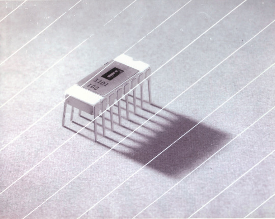

This one is cool because it's cute. Look at that. This thing was completely hand-designed by engineers drawing the shapes of transistor gates on sheets of overhead transparency and exposing pieces of crudely spun silicon to light in a """"cleanroom"""" that would cause most modern fab equipment to swoon like a delicate Victorian lady. Semiconductor manufacturing was maturing at this point but a fab still had more in common with a darkroom for film development than with the mega expensive building sized machines we use today.
As that link above notes, these things were really rough and tumble, and designs were being updated on the scale of weeks as Intel learned, well, how to make chips at an industrial scale. They weren't the first company to do this, in the 60's you could run a chip fab out of a sufficiently well sealed garage, but they were busy building the background that would lead to the next sixty years.
Lisp Chips
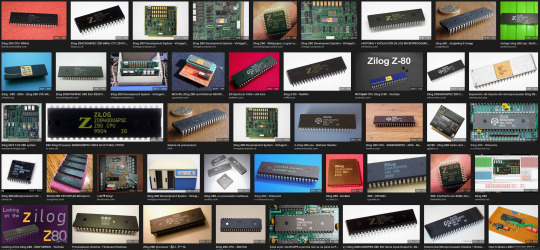
This is a family of utterly bullshit prototype processors that failed to be born in the whirlwind days of AI research in the 70's and 80's.
Lisps, a very old but exceedingly clever family of functional programming languages, were the language of choice for AI research at the time. Lisp compilers and interpreters had all sorts of tricks for compiling Lisp down to instructions, and also the hardware was frequently being built by the AI researchers themselves with explicit aims to run Lisp better.
The illogical conclusion of this was attempts to implement Lisp right in silicon, no translation layer.
Yeah, that is Sussman himself on this paper.
These never left labs, there have since been dozens of abortive attempts to make Lisp Chips happen because the idea is so extremely attractive to a certain kind of programmer, the most recent big one being a pile of weird designd aimed to run OpenGenera. I bet you there are no less than four members of r/lisp who have bought an Icestick FPGA in the past year with the explicit goal of writing their own Lisp Chip. It will fail, because this is a terrible idea, but damn if it isn't cool.
There were many more chips that bridged this gap, stuff designed by or for Symbolics (like the Ivory series of chips or the 3600) to go into their Lisp machines that exploited the up and coming fields of microcode optimization to improve Lisp performance, but sadly there are no known working true Lisp Chips in the wild.
Zilog Z80
Perhaps the most important chip that ever just kinda hung out. The Z80 was almost, almost the basis of The Future. The Z80 is bizzare. It is a software compatible clone of the Intel 8080, which is to say that it has the same instructions implemented in a completely different way.
This is, a strange choice, but it was the right one somehow because through the 80's and 90's practically every single piece of technology made in Japan contained at least one, maybe two Z80's even if there was no readily apparent reason why it should have one (or two). I will defer to Cathode Ray Dude here: What follows is a joke, but only barely

The Z80 is the basis of the MSX, the IBM PC of Japan, which was produced through a system of hardware and software licensing to third party manufacturers by Microsoft of Japan which was exactly as confusing as it sounds. The result is that the Z80, originally intended for embedded applications, ended up forming the basis of an entire alternate branch of the PC family tree.
It is important to note that the Z80 is boring. It is a normal-ass chip but it just so happens that it ended up being the focal point of like a dozen different industries all looking for a cheap, easy to program chip they could shove into Appliances.
Effectively everything that happened to the Intel 8080 happened to the Z80 and then some. Black market clones, reverse engineered Soviet compatibles, licensed second party manufacturers, hundreds of semi-compatible bastard half-sisters made by anyone with a fab, used in everything from toys to industrial machinery, still persisting to this day as an embedded processor that is probably powering something near you quietly and without much fuss. If you have one of those old TI-86 calculators, that's a Z80. Oh also a horrible hybrid Z80/8080 from Sharp powered the original Game Boy.
I was going to try and find a picture of a Z80 by just searching for it and look at this mess! There's so many of these things.
I mean the C/PM computers. The ZX Spectrum, I almost forgot that one! I can keep making this list go! So many bits of the Tech Explosion of the 80's and 90's are powered by the Z80. I was not joking when I said that you sometimes found more than one Z80 in a single computer because you might use one Z80 to run the computer and another Z80 to run a specialty peripheral like a video toaster or music synthesizer. Everyone imaginable has had their hand on the Z80 ball at some point in time or another. Z80 based devices probably launched several dozen hardware companies that persist to this day and I have no idea which ones because there were so goddamn many.
The Z80 eventually got super efficient due to process shrinks so it turns up in weird laptops and handhelds! Zilog and the Z80 persist to this day like some kind of crocodile beast, you can go to RS components and buy a brand new piece of Z80 silicon clocked at 20MHz. There's probably a couple in a car somewhere near you.
Pentium (P6 microarchitecture)
Yeah I am going to bring up the Hackers chip. The Pentium P6 series is currently remembered for being the chip that Acidburn geeks out over in Hackers (1995) instead of making out with her boyfriend, but it is actually noteworthy IMO for being one of the first mainstream chips to start pulling serious tricks on the system running it.

The P6 microarchitecture comes out swinging with like four or five tricks to get around the numerous problems with x86 and deploys them all at once. It has superscalar pipelining, it has a RISC microcode, it has branch prediction, it has a bunch of zany mathematical optimizations, none of these are new per se but this is the first time you're really seeing them all at once on a chip that was going into PC's.
Without these improvements it's possible Intel would have been beaten out by one of its competitors, maybe Power or SPARC or whatever you call the thing that runs on the Motorola 68k. Hell even MIPS could have beaten the ageing cancerous mistake that was x86. But by discovering the power of lying to the computer, Intel managed to speed up x86 by implementing it in a sensible instruction set in the background, allowing them to do all the same clever pipelining and optimization that was happening with RISC without having to give up their stranglehold on the desktop market. Without the P5 we live in a very, very different world from a computer hardware perspective.
From this falls many of the bizzare microcode execution bugs that plague modern computers, because when you're doing your optimization on the fly in chip with a second, smaller unix hidden inside your processor eventually you're not going to be cryptographically secure.
RISC is very clearly better for, most things. You can find papers stating this as far back as the 70's, when they start doing pipelining for the first time and are like "you know pipelining is a lot easier if you have a few small instructions instead of ten thousand massive ones.
x86 only persists to this day because Intel cemented their lead and they happened to use x86. True RISC cuts out the middleman of hyperoptimizing microcode on the chip, but if you can't do that because you've girlbossed too close to the sun as Intel had in the late 80's you have to do something.
The Future
This gets us to like the year 2000. I have more chips I find interesting or cool, although from here it's mostly microcontrollers in part because from here it gets pretty monotonous because Intel basically wins for a while. I might pick that up later. Also if this post gets any longer it'll be annoying to scroll past. Here is a sample from a post I have in my drafts since May:

I have some notes on the weirdo PowerPC stuff that shows up here it's mostly interesting because of where it goes, not what it is. A lot of it ends up in games consoles. Some of it goes into mainframes. There is some of it in space. Really got around, PowerPC did.
236 notes
·
View notes
Text
TSMC will invest an additional $100 billion in Arizona, add 3 facilities
Following a meeting at the White House today, President Trump and TSMC Chairman and CEO C.C. Wei announced a historic expansion of TSMC’s advanced semiconductor operations in Arizona. TSMC will invest at least an additional $100 billion to build three additional semiconductor fabs in Arizona as well as an advanced packaging facility and R&D Center. The investment comes in addition to TSMC’s three fabs already in operation or under construction in Arizona and will represent thousands of additional new jobs.
TSMC announced its first fab in Arizona in May 2020. Since then, its presence has grown to three cutting-edge chip-making fabs and supporting facilities, representing a $65 billion investment and 6,000 jobs. Today’s announcement brings TSMC’s total announced investment in Arizona to $165 billion.
In January, TSMC announced it had begun producing advanced 4-nanometer chips for U.S. customers in Arizona, a first on American soil and a major milestone in the country’s efforts to reshore manufacturing of the most advanced microchips. Its second fab, which is under construction, is expected to produce the world’s most advanced 2nm process technology with next generation nanosheet transistors in addition to the previously announced 3nm technology. TSMC’s third fab will produce chips using 2nm or more advanced processes, with production beginning by the end of the decade.
“TSMC’s historic announcement cements Arizona as the epicenter of advanced chip manufacturing and innovation in America,” said Governor Katie Hobbs. “With the country’s most advanced chip-making processes, world class university partners, and a robust and growing talent pipeline, Arizona is powering the groundbreaking technologies of the future like AI. I’m grateful to President Trump, TSMC, and all our partners for making this historic day possible.”
Through this expansion, TSMC expects to create hundreds of billions of dollars in semiconductor value for AI and other cutting-edge applications. TSMC’s expanded investment is expected to support 40,000 construction jobs over the next four years and create tens of thousands of high-paying, high-tech jobs in advanced chip manufacturing and R&D. It is also expected to drive more than $200 billion of indirect economic output in Arizona and across the United States in the next decade. This move underscores TSMC’s dedication to supporting its customers, including America’s leading AI and technology innovation companies such as Apple, NVIDIA, AMD, Broadcom, and Qualcomm.
9 notes
·
View notes
Text
5amsůng's 'HBM delay' in the news now is pretty related to my work. We're very very very late. We were supposed to deliver last October. We create a unit, it gets tested by the semiconductor fabs, then it gets mass produced. We're still in testing phase. The technology is proven. We just have to work out all the bugs. Make it safe and reliable. There are very high wattages and voltages involved, and big risk to pretty all the equipment connected to it, and everyone nearby it. Also, we're using a patented new water cooled heatsink design with over 100 potential failure points. Why? To create a chip that costs hundreds of thousands of dollars a pop. Because we have to do it before someone else does, or we'll lose money, security, and power. The reason we do anything, tbh. No pressure!
2 notes
·
View notes
Text
The Biden administration recently promised it will finally loosen the purse strings on $39 billion of CHIPS Act grants to encourage semiconductor fabrication in the U.S. But less than a week later, Intel announced that it’s putting the brakes on its Columbus factory. The Taiwan Semiconductor Manufacturing Company (TSMC) has pushed back production at its second Arizona foundry. The remaining major chipmaker, Samsung, just delayed its first Texas fab. This is not the way companies typically respond to multi-billion-dollar subsidies. So what explains chipmakers’ apparent ingratitude? In large part, frustration with DEI requirements embedded in the CHIPS Act. Commentators have noted that CHIPS and Science Act money has been sluggish. What they haven’t noticed is that it’s because the CHIPS Act is so loaded with DEI pork that it can’t move.
…
Handouts abound. There’s plenty for the left—requirements that chipmakers submit detailed plans to educate, employ, and train lots of women and people of color, as well as “justice-involved individuals,” more commonly known as ex-cons. There’s plenty for the right—veterans and members of rural communities find their way into the typical DEI definition of minorities. There’s even plenty for the planet: Arizona Democrats just bragged they’ve won $15 million in CHIPS funding for an ASU project fighting climate change. That project is going better for Arizona than the actual chips part of the CHIPS Act. Because equity is so critical, the makers of humanity’s most complex technology must rely on local labor and apprentices from all those underrepresented groups, as TSMC discovered to its dismay. Tired of delays at its first fab, the company flew in 500 employees from Taiwan. This angered local workers, since the implication was that they weren’t skilled enough. With CHIPS grants at risk, TSMC caved in December, agreeing to rely on those workers and invest more in training them. A month later, it postponed its second Arizona fab. Now TSMC has revealed plans to build a second fab in Japan. Its first, which broke ground in 2021, is about to begin production. TSMC has learned that when the Japanese promise money, they actually give it, and they allow it to use competent workers. TSMC is also sampling Germany’s chip subsidies, as is Intel.
…
In short, the world’s best chipmakers are tired of being pawns in the CHIPS Act’s political games. They’ve quietly given up on America. Intel must know the coming grants are election-year stunts — mere statements of intent that will not be followed up. Even after due diligence and final agreements, the funds will only be released in dribs and drabs as recipients prove they’re jumping through the appropriate hoops. For instance, chipmakers have to make sure they hire plenty of female construction workers, even though less than 10 percent of U.S. construction workers are women. They also have to ensure childcare for the female construction workers and engineers who don’t exist yet. They have to remove degree requirements and set “diverse hiring slate policies,” which sounds like code for quotas. They must create plans to do all this with “close and ongoing coordination with on-the-ground stakeholders.” No wonder Intel politely postponed its Columbus fab and started planning one in Ireland. Meanwhile, Commerce Secretary Gina Raimondo was launching a CHIPS-funded training program for historically black colleges.
…
This is the stuff declining empires are made of. As America pursues national security by building a diverse workforce, China does it by building warships. The CHIPS Act’s current identity as a jobs program for favored minorities means companies are forced to recruit heavily from every population except white and Asian men already trained in the field. It’s like fishing in all the places you aren’t getting bites.
4 notes
·
View notes
Text
The Future of Semiconductors: Unveiling a World of Possibilities
**The Future of Semiconductors: Unveiling a World of Possibilities**
As we stand on the brink of a new era, the semiconductor industry finds itself at the heart of a technological revolution. The impact of semiconductors on our lives has been profound, driving advancements across industries and shaping the very fabric of our modern civilization. But what lies ahead for this dynamic and transformative field? Let's delve into the future of semiconductors and the boundless possibilities that await us.
**1. Quantum Leap in Computing:**
The race towards quantum computing is intensifying, and semiconductors will play a pivotal role in unlocking its true potential. Quantum processors, built on novel semiconductor materials, have the power to process vast amounts of data in a fraction of the time it takes traditional computers. The future of computing will transcend current limitations, empowering us to solve complex problems previously deemed insurmountable.
**2. AI and Machine Learning:**
The era of artificial intelligence is upon us, and semiconductors will serve as the backbone of AI and machine learning applications. With the growing demand for AI-driven technologies in autonomous vehicles, robotics, healthcare, and more, the semiconductor industry is set to witness an unprecedented surge in AI-focused chip designs. Neuromorphic computing, inspired by the human brain's architecture, could unlock revolutionary AI capabilities, paving the way for cognitive computing and self-learning systems.
**3. The Internet of Things (IoT) Revolution:**
As IoT proliferates, the demand for energy-efficient and high-performance semiconductor devices will skyrocket. We envision a future where billions of interconnected devices communicate seamlessly, facilitated by advanced semiconductor technologies. Ultra-low-power processors, sensors, and wireless communication chips will define the landscape of the IoT revolution, shaping smart cities, wearables, and an interconnected world.
**4. Green and Sustainable Semiconductors:**
Sustainability will be a driving force in the semiconductor industry's future. Innovations in materials and manufacturing processes will lead to environmentally friendly and energy-efficient semiconductor solutions. From eco-friendly chip packaging to renewable energy-powered fabs, the industry will strive to minimize its carbon footprint, contributing to a greener tomorrow.
**5. Silicon Photonics and Beyond:**
The integration of photonics with silicon promises a new era of ultra-high-speed data transmission and processing. Silicon photonics will revolutionize data centers, enabling faster communication between chips and reducing data bottlenecks. Moreover, emerging technologies like 2D materials and carbon nanotubes offer exciting possibilities for futuristic semiconductor devices that could outperform traditional silicon-based chips.
**6. Security and Privacy:**
With the increasing dependence on connected devices, security and privacy will be paramount. Future semiconductor designs will prioritize hardware-based security features to protect against cyber threats and safeguard sensitive data. Trusted execution environments and secure enclaves will become integral components of semiconductor devices, ensuring user confidence in an interconnected world.
**7. Global Collaboration and Talent Development:**
The future of semiconductors will thrive on global collaboration and talent development. International partnerships will foster innovation, as countries pool their resources and expertise. Companies will invest in nurturing a diverse and skilled workforce, driving advancements and promoting a culture of inclusion and creativity.
The future of semiconductors is bright, brimming with possibilities that have the potential to redefine our world. As innovators, engineers, and visionaries, let's embrace this transformative journey together. Let's harness the power of semiconductors to build a future that empowers, connects, and inspires generations to come.
*The future is here, and it's in the hands of those who dare to dream and innovate with semiconductors as their guiding light.*
2 notes
·
View notes
Text
I thought I would hate factory work, but working in a semiconductor fab is tje best job ive had.
I am respected, I have autonomy in getting my work done. I get a comfy chair and am not expected to be doing anything if I do not currently have any work to do.
Our manager asks what he can do for us far more often than he tells us what to do.
Its incredible how much difference some minor changes in workplace policy and mindset can make.
The reason people don’t want to work is that it’s just normal for them to be in bad work environments.
My issue with working at Walmart wasn’t the work itself I was doing. It was the circumstances around it. The concrete floor, lack of places to sit, having to put up with asshole customers, not getting time off for injuries, and bad pay.
If I had been given shock pads to stand on or a few chairs to rest on sometimes, if they paid me a livable amount of money and I was allowed to yell back at asshole customers, if they had given me any amount of training, I would happily work part time folding clothes all day and telling people where the swimsuit section is.
I’m a creative type. I’m a writer. I’m pretty smart, even. But if I could make a living folding shirts and listening to podcasts in one ear and helping people find the scented candles for 30 hours a week? I would. Leaves some mental space free for me to brainstorm. Lets me catch up on my reading with audiobooks.
But instead I was treated so badly by upper management and customers that I’m like legitimately a little frightened whenever I step into a Walmart now. And I only worked there for three months a few years ago.
I’m a good lower level worker. When I’m treated well. I like finishing tasks. I like being helpful. I like having some time to talk to coworkers and some time alone with my thoughts. I’m a frickin team player. And that’s how I was at my first job. I was treated well by my supervisor. I was trained. They were patient with me. I was so good at being low on the totem pole at that job because I was valued and felt like I was being listened to. I was able to sit still when there was nothing left to do which made it feel less bad when we were on a time crunch. I didn’t mind working hard at that job because it was fun even though I was doing all the low level stuff that the supervisors didn’t want do.
But at Walmart I was like that for all of two days. Then I figured out that nobody appreciated my work and if I worked in my normal people pleasing manner I’d kill myself because their standards were high and the rewards for meeting them were low.
So I slowed down. I started avoiding customers. I started taking a lot longer to get to my breaks and to come back from them. I became worse at my job because no matter how good I was at it there would be no reward, no appreciation, and I’d just be pushed further beyond my limits.
My only level of happiness from that job came from the people who were working with me. The old ladies and my department manager who made sure I wasn’t overextending myself. The one other young man working in the clothing department who always got sent with me to unload the heavy stuff and commiserated with me about the shoulder injuries, the hurting feet we were too young to have.
But none of that was enough to make me stay. We were constantly understaffed. I was constantly abused by customers and not able to do a thing about it. I was not paid much at all. So as soon as I had enough saved up for what I was trying to do and my last semester of college was about to start I handed in my two weeks.
I would have found a way to stay if I liked that job. If I liked that job I would’ve pushed myself to my mental limits to finish college and keep that job at the same time. Heck that job could’ve been a rest from college. A place to get away from it. But I hate that job so I got out as soon as I could.
I want to work. I want enough money to live sort of comfortably. I want to have some tasks to do to give my creativity a rest. I want to be a part of something. But the way that modern corporate run work environments are set up does not give me any of the things I actually want out of a job. And I think that’s the same for millions of people right now. A lot of people would happily spend their lives as a waitress or an Uber driver or a warehouse worker or a farmhand or any other “low skill” job you can possibly think of. But with the way the world works right now those jobs are absolutely miserable. It doesn’t have to be that way. I know because I’ve had a fulfilling part time minimum wage job that I looked forward to going to every week. A job where I was listened to and allowed to sit when I needed to. I miss that job. Especially now since I’ve realized that’s not the standard. It should be. People should look forward to going to work or at the very least not get mild ptsd whenever they set foot into a Walmart.
22K notes
·
View notes
Text
The Revolutionary Application of Quartz Plate in Semiconductor Packaging
The Revolutionary Application of Quartz Plate in Semiconductor Packaging: Why These Four Designs Are Game-Changers Let’s cut through the noise: semiconductor packaging isn’t just about chips anymore—it’s about the materials that cradle them. Quartz plates, once relegated to lab equipment, are now the unsung heroes of microelectronics. But not all quartz is created equal.
I’ve seen firsthand how four specific designs—round transparent quartz glass plates, tempered quartz sight glass, OEM customized optical square/round quartz glass plates, and square UV transparent quartz plates—are rewriting the rules of reliability and precision. Here’s why they matter.
1. Round Transparent Quartz Glass Plates: The Purity Powerhouse
Imagine a material so pristine it makes surgical steel look rusty. Round transparent quartz plates, with >99.99% SiO₂ purity, are the gold standard for wafer handling in extreme environments. Take TSMC’s 3nm node fab: by replacing ceramic carriers with these plates, they reduced particulate contamination by 78% during high-temperature annealing1. The secret? Zero metallic ions means no unwanted doping—critical when a single stray atom can wreck a billion-transistor chip.
But purity isn’t their only trick. Their thermal stability (up to 1,200°C) allows rapid thermal processing (RTP) cycles without warping—a feat that aluminum nitride plates fail at after 50 cycles.
2. Tempered Quartz Sight Glass: When Failure Isn’t an Option
Vacuum chambers in EUV lithography systems demand visibility and invincibility. Tempered quartz sight glass, chemically strengthened via ion exchange, laughs at 10⁻⁸ Torr pressures while providing distortion-free inspection windows. ASML’s latest EUV machines use these panels to monitor plasma arcs—where standard fused silica would cloud within weeks under 13.5nm radiation.
The kicker? Their surface hardness (9 Mohs) prevents scratches from robotic handlers—eliminating the “fogged window” failures that once caused 12% of lithography tool downtime.
3. OEM Customized Optical Square/Round Quartz Plates: Geometry Meets Photonics
Why settle for off-the-shelf when light manipulation demands perfection? Customized optical quartz plates, with sub-λ/4 flatness, are enabling breakthroughs in chip-scale photonics. Intel’s optical interconnects team credits square quartz plates—etched with nanoscale grating patterns—for achieving 92% light coupling efficiency in their silicon photonics modules12. The rectangular edges align perfectly with waveguide arrays, something round plates can’t match.
But round variants shine too: their radial symmetry minimizes stress birefringence in laser diode packaging—a must for 800G DR4 transceivers.
4. Square UV Transparent Quartz Plates: The Dark Horse of Advanced Packaging
UV-curing adhesives are the glue holding 2.5D/3D packages together—literally. Square UV quartz plates, transmitting >90% at 254nm, ensure uniform curing while blocking IR heat that warps interposers. Samsung’s HBM4 stack line reported a 30% yield boost after switching to these plates, as their sharp corners align with die edges to prevent adhesive bleed-out.
Bonus: Their UV transparency doubles as a built-in quality check—uncured resin fluoresces under 365nm light, visible through the plate.

Why This Isn’t Just Progress—It’s a Paradigm Shift
Critics argue quartz is “too brittle” or “too niche.” Tell that to the engineers who’ve seen:
Round plates slash cleanroom particle counts by filtering airborne contaminants during robotic transfers.
Square UV plates enable fan-out wafer-level packaging (FOWLP) for wearables, where 0.1mm thickness tolerances are non-negotiable.
While graphene and GaN hog headlines, quartz plates work silently in the trenches—enabling the angstrom-scale precision our connected world demands.
The Bottom Line In semiconductor packaging, the difference between “functional” and “flawless” lies in the materials you trust. These four quartz plate designs aren’t just components—they’re enablers of a future where chips aren’t just smaller, but smarter. If your supply chain hasn’t embraced them yet, you’re not just behind the curve—you’re ignoring the bedrock of modern electronics.
0 notes
Text
What is SECS/GEM? Understanding the SEMI Equipment Communications Standard/Generic Equipment Model
#secs/gem#secs/gem software#semiconductor#equipment software#secs gem software#secs/gem protocol#fab automation
0 notes
Text
0 notes
Text
I kind of want to go off a bit about Lynn Conway's technical contributions, because somehow, "your smartphone would not exist without her work" is actually underselling it. And I thought I appreciated Conway's work, but when I went digging I found some things I'd never even heard about.
First of all, before any of the work she's most famous for, before IBM fired her for being trans, she worked on IBM's Advanced Computer Systems project, the team tasked with trying to beat Seymour Cray and his team at CDC in their continuing quest to build the fastest computers in the world. As part of the project, she invented dynamic instruction scheduling, which is crucial to every modern high-performance CPU. The project might have actually succeeded in beating CDC if it hadn't been killed, but that's another story.
And because one crucial innovation that defines modern microprocessor design apparently wasn't enough, she then worked on VLSI. The techniques she helped to pioneer in chip design don't just power your phone: Her work underpins almost every modern microchip. CPUs, GPUs, ASICs, everything. It was a revolution. That's not just my opinion, the wikipedia page literally has "revolution" in the title.
I also want to be very clear why I mean by "helped to pioneer", because a lot of subsequent accounts have diminished Conway's role in her own research: the VLSI work was a collaboration between Xerox PARC and Caltech, with Lynn Conway being the lead on the PARC side and Carver Mead being the lead on the Caltech side, with Mead being the physics expert and Conway being the computer architecture expert (which is an appropriate role for the inventor of dynamic instruction scheduling). While Mead had already been doing work on VLSI, Conway was not an assistant or subordinate: she was the co-lead, and a lot of VLSI innovations came directly from her, with scalable design rules being one her more frequently cited contributes (I'm a little bit out of my depth on the specifics of VLSI, being a programmer and all, so I'm not digging too deep here).
But of equal importance to her work on developing VLSI techniques was her work on teaching them. Developing a textbook on VLSI was her idea, and the result was Introduction to VLSI Systems. As part of the development process, she taught a course at MIT based on a draft of the book. That book and her course soon formed the basis for VLSI courses around the country. And because that apparently wasn't enough, as a part of that MIT course she also created MPC79, the first multi-project chip service (multi-project chip services combine a bunch of different microchip designs together into one large chip design before sending it out to a fab to be manufactured), making it economical for students' chip designs to be fabricated and shipped back to them. MPC79 was the direct inspiration for the DARPA-funded MOSIS, which provided access to chip fabrication to students and researchers across the country.
The VLSI tools and techniques made chip design a lot easier and much more accessible. Combined with MPC79/MOSIS granting broader access to chip manufacturing, there was a flood of students and researchers doing pioneering hardware design work. Sun's workstations, SGI's 3D graphics hardware, the SPARC and MIPS CPUs, all of these began life as VLSI projects at universities that were prototyped with MCP services. And while those are big, high-profile examples of early projects enabled by Conway's work, There are many, many more, far too many to count, and that number only gets bigger as you move forward through the years, until it encompasses almost everything the semiconductor industry creates.
And that's just her technical work. Her trans activism work in the 2000s was incredibly significant, and her website is frankly amazing. Her efforts to get other female and minority STEM pioneers the recognitions they rightly deserve are also worth remembering.

Goodbye, Lynn. Thank you for your constant support and encouragement since the day I started these comics. It has meant the world to me, and I wish I could have told you. We will remember you forever.
64K notes
·
View notes
Text
Semiconductor Chemicals Market Growth Driven by Advanced Manufacturing and Technological Innovations Worldwide
The semiconductor chemicals market is experiencing significant growth, driven by the rising demand for advanced electronic components. As semiconductor technology evolves, the need for high-purity chemicals used in wafer processing, etching, and cleaning is increasing. Factors such as the expansion of 5G networks, artificial intelligence, and the Internet of Things (IoT) are fueling this demand. Additionally, the push for miniaturization and enhanced performance in semiconductor devices requires highly specialized chemicals that ensure precision and efficiency in manufacturing.

Rising Demand for High-Purity Chemicals
High-purity chemicals are essential in semiconductor fabrication, as even the slightest contamination can impact chip performance. Chemical solutions used in photolithography, wet etching, and deposition processes must meet stringent purity standards. As semiconductor nodes shrink to below 5 nanometers, the demand for ultra-high purity chemicals continues to rise. Manufacturers are investing in advanced purification technologies to meet the growing need for these specialized materials, ensuring defect-free chip production.
Impact of Advanced Technologies on Market Growth
The adoption of cutting-edge technologies, including extreme ultraviolet (EUV) lithography and advanced packaging techniques, is reshaping the semiconductor industry. These innovations require new chemical formulations that enhance precision and efficiency. EUV lithography, for instance, relies on advanced photoresists and etching solutions to enable next-generation chip designs. The shift toward 3D chip architectures and heterogeneous integration is also driving the need for novel chemical compositions that support improved conductivity, durability, and performance.
Supply Chain Challenges and Market Expansion
Global supply chain disruptions have affected the semiconductor industry, including the availability of key chemical materials. The rising cost of raw materials, geopolitical tensions, and transportation constraints have led to supply fluctuations. To mitigate these challenges, companies are investing in localized production facilities and strategic partnerships with chemical suppliers. Governments are also implementing policies to support domestic semiconductor production, further boosting demand for semiconductor chemicals in various regions.
Sustainability and Eco-Friendly Chemical Solutions
Sustainability is becoming a major focus in the semiconductor industry, with increasing efforts to reduce environmental impact. The shift toward eco-friendly chemical solutions is gaining momentum, as companies strive to minimize hazardous waste and energy consumption. Green chemistry innovations, such as water-based cleaning solutions and biodegradable etching agents, are being developed to align with sustainability goals. Additionally, regulatory frameworks are encouraging the adoption of environmentally friendly materials, shaping the future of the semiconductor chemicals market.
Growth Opportunities in Emerging Markets
Asia-Pacific remains the dominant region for semiconductor manufacturing, with countries like China, South Korea, and Taiwan leading the industry. However, other regions, including North America and Europe, are ramping up their semiconductor production capabilities. The growing investments in semiconductor fabs and R&D initiatives in these regions present new opportunities for chemical suppliers. The increasing demand for consumer electronics, automotive semiconductors, and industrial automation is further driving market expansion globally.
Conclusion
The semiconductor chemicals market is evolving rapidly, driven by technological advancements, supply chain adaptations, and sustainability efforts. The rising demand for high-purity chemicals, coupled with the adoption of advanced manufacturing techniques, is shaping the future of the industry. As semiconductor manufacturers push the boundaries of innovation, chemical suppliers will play a critical role in enabling the next generation of high-performance electronic devices.
0 notes