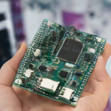
#SRAM interface
Explore tagged Tumblr posts
Visit Tumblr Blog
Explore Tumblr blogs with no restrictions, modern design and the best experience.
Last Seen Tumblr Blogs


Fun Fact
Tumblr is available in 18 languages.
Text
Memory ICs, SRAM memory chips, SRAM chip programming, SRAM interface
CY62157E Series 8 Mb (512 K x 16) 4.5 - 5.5 V 45 ns Static RAM - TSOP-44
0 notes
Text
https://www.futureelectronics.com/p/semiconductors--memory--RAM--static-ram--asynchronous/cy62167ev30ll-45bvxit-infineon-8026254
SRAM memory card, SRAM memory chips, Static ram, SRAM memory
CY62167EV30 Series 16 Mb (1M x 16 / 2 M x 8) 3 V 45 ns Static RAM - FBGA-48
#Infineon#CY62167EV30LL-45BVXIT#RAM#Static RAM Asynchronous#SRAM#memory card#chips#SRAM memory#Non Volatile SRAM#SRAM chip#Static ram manufacturers#asynchronous memory interface#SRAM in microprocessor
1 note
·
View note
Text
Wrap030-ATX Remembers
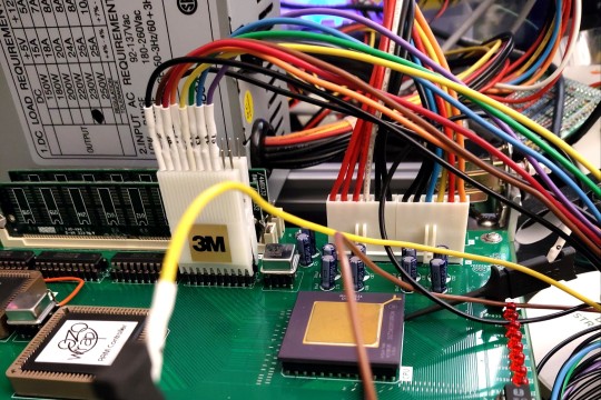
No general-purpose computer will do much without a good amount of Random Access Memory for transient storage of code and data. Now that I have confirmed basic operation of CPU, bus controller, ROM, and serial, it's time to turn my attention to main system memory.
Every homebrew computer I've built to date, including previous iterations of the Wrap030 project, has used Static RAM. Static RAM is nearly as simple as peripherals can be — give it an address, assert a Chip Enable and a Read or Write strobe signal, wait a bit, and release. Done, cycle complete. If you don't need to retrieve some data for a good long while, it's no matter so long as the chip still has power. For a small system, SRAM is reliable and dead simple to use.
The problem with SRAM is it is also very expensive. The 2MB of SRAM I had on the previous iteration of Wrap030 cost over $20 — and it's still far from enough to run an operating system like Unix System V, NetBSD, Linux, etc. This is the reason computers generally use Dynamic RAM for primary system memory.
The difference is SRAM uses several transistors to create a flip-flop for storing each and every bit of memory, whereas DRAM uses a capacitor to store each bit of memory. This reduces manufacturing costs and increases storage density, but does come with some trade-offs. Most notably, the capacitors that store bits in DRAM will lose their charge — and the stored data with it — after a rather brief period of time. This means the DRAM capacitors need to be topped off regularly in a process known as a refresh cycle.
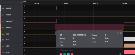
Another complication of using DRAM is the bus interface has been changed to allow much larger storage capacities without the physical chip package growing to absurd sizes. Instead of the chip accepting the entire address at once, it expects to be given a Row address (along with a Row Address Strobe [RAS#]) then a Column address (along with a Column Address Strobe [CAS#]), with myriad specific timing requirements for when each signal should be asserted and deasserted.
In short, DRAM is much more difficult to interface with compared to SRAM, so I've never really gotten around to it.
With one of the long term goals of this project being running a *nix operating system though, I'm going to need the larger memory that DRAM affords. So i made provision for a CPLD to serve as a dedicated DRAM controller on the Wrap030-ATX motherboard and added a couple 72-pin SIMM slots. In theory this setup should be able to support up to 256MB of RAM (if rare 128MB SIMMs should fall into my hands...).
So where do we turn when dealing with complicated timing with multiple modes and a bunch of I/O? Why, Finite State Machines, of course! That bit where the DRAM expects a row address for a little while, that's a state. And the following bit where the DRAM expects a column address is another state. And then another state to make sure the DRAM has enough time to write or fetch the data. The round it out with one last state to tell the CPU data is ready.
What about that weird refresh timing? Well, that's just few more states for the state machine. And then one last "idle" state that waits for a refresh timing counter to hit 0 or for the CPU to start a bus cycle. Laid out like that, the DRAM controller became a state machine with 7 or 8 states, a counter, and an address multiplexer.
The logic actually came together easier than expected. Not completely without bugs of course.
There's this note in the datasheets about startup initialization where the DRAM should not be accessed 200μs after power on, and there should be 8 refresh cycles before the first access. Initially I had built this entire sequence into my logic. It consumed a ton of resources and didn't really work right.
I realized that my reset circuit held the CPU in reset for longer than 200μs on power on, so I was guaranteed that first initialization time. So I removed that startup delay from my DRAM controller logic, and made a few tweaks to the state machine so it could do 8 back-to-back refresh cycles after reset.
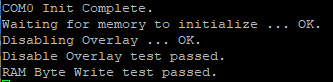
I was able to successfully write to DRAM and read that data back!
That much proved to be the easy part. The next steps were confirming DRAM accesses worked reliably, that I had the order of my byte select signals correct, that I could identify the amount of installed memory, and that all of the installed memory was working. These are programming problems, not logic problems, and I am not a strong programmer. On top of that, not only am I working with unproven DRAM logic, but I'm also using untested SIMMs that I had picked up from Computer Reset.
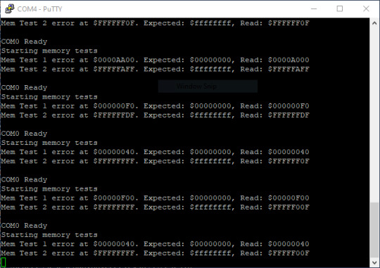
I quickly ran into errors, but was it a problem with my logic? A problem with my timing? A problem with the SIMMs?
I had a large back of 72-pin SIMMs, split fairly evenly between Fast Page Mode (FPM) and Extended Data Output (EDO) types. I tried them all. Some would pass the tests for nearly all addresses but fail at the end. Some seemed to have a stuck bit. Some were just plain bad and gave errors everywhere. It didn't really answer the question about whether my logic was bad, but results were consistent enough for me to think that maybe the logic might be ok.
And then finally I came across a pair of HP-branded 8MB EDO SIMMs that passed a simple write-read test without error ...
... right around the time my serial port stopped working. But the memory test was passing, and I could at least see the serial output on the logic analyzer.
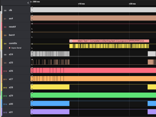
The serial port problem was a bit setback. It had been working but suddenly wasn't. Clearly the UART itself was working, I just wasn't getting anything past the level shifter. Well that at least gave me a starting point of where to look. Sure enough, one of the 12V supply pins was not well soldered. Thankfully a quick fix.
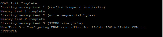
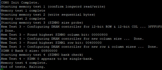
Back to testing memory, I started writing a program to identify the size of the installed SIMM and write a register I added to the DRAM controller to configure the specific geometry of the installed memory. See, DRAM has another lovely quirk — chips of the same size may have a different configuration of Row and Column sizes. For instance one chip may have a 9-bit Column and a 10-bit Row, but the next may have a 10-bit Column and a 9-bit Row, and both are the same size. If the DRAM controller just assumes 12-bit Row and Column (the largest supported by 72-pin SIMMs), then there will be gaps in the memory map that will need to be accounted for in software (using MMU, for example). If the DRAM controller knows the geometry of the installed memory, then it can present the memory to the CPU as one contiguous block of memory.
And that's where I found my next bug. The system would just hang when trying to write to that DRAM controller configuration register.
... because I had forgotten to complete that part of the state machine. The result was the state machine would end up in a state for writing to the configuration register, but then it couldn't get out of it. Once I added the missing condition to the state machine logic I was able to correctly identify the geometry and size for my installed memory!
Wow that was long. This has been the biggest, most involved step in the process of bringing up this computer yet. It turns out there are a lot of moving pieces that have to all work together to get the computer running code from ROM and reading/writing DRAM.
Now that I have my main memory working, I should be able to get some software running. I'm hoping to at least have BASIC running in time for VCFSW at the end of June.
#homebrew computing#vintage computing#motorola#mc68030#motorola 68k#assembly programming#motorola 68030#vcf#VCFSW#vcf southwest#verilog#Dynamic RAM#CPLD#troubleshooting#wrap030 atx
32 notes
·
View notes
Text
Arduino Due vs. Mega: A Comprehensive Comparison
What is Arduino Due and Mega?
The Arduino platform has revolutionized the world of DIY electronics, providing hobbyists and professionals alike with versatile and powerful microcontroller boards. Among the myriad of options, the Arduino Due and Arduino Mega stand out for their advanced features and robust performance. The Arduino Due, introduced in 2012, is the first Arduino board based on a 32-bit ARM core microcontroller, the Atmel SAM3X8E. In contrast, the Arduino Mega, built around the 8-bit ATmega2560 microcontroller, is known for its abundant I/O pins and memory. Understanding the differences between these two boards can help in selecting the right one for specific projects, enhancing both functionality and efficiency.
Processing Power and Performance
The processing capabilities of the Arduino Due and Mega are distinctly different, primarily due to their core microcontrollers. The Arduino Due, with its 32-bit ARM Cortex-M3 processor running at 84 MHz, offers significantly higher processing power compared to the Arduino Mega's 8-bit ATmega2560, which operates at 16 MHz. This difference in architecture and clock speed means that the Due can handle more complex calculations and tasks faster and more efficiently than the Mega. For projects requiring high computational power, such as real-time data processing or handling multiple sensors simultaneously, the Due is the superior choice. However, for simpler tasks, the Mega's processing power may suffice.
Memory and Storage Capabilities
Memory is another critical aspect where the Arduino Due and Mega diverge. The Arduino Due is equipped with 512 KB of flash memory for code storage and 96 KB of SRAM for data. On the other hand, the Arduino Mega has 256 KB of flash memory and 8 KB of SRAM. Additionally, the Due features a Direct Memory Access (DMA) controller, which allows for efficient memory operations, freeing up the CPU to handle other tasks. These memory enhancements make the Due more suitable for applications requiring large codebases and significant data handling, such as advanced robotics or sophisticated control systems. The Mega, with its more modest memory, is ideal for less demanding applications.
Input/Output Capabilities and Expansion
Both the Arduino Due and Mega are renowned for their extensive input/output (I/O) capabilities, yet they cater to different needs. The Mega boasts a whopping 54 digital I/O pins, 16 analog inputs, and 4 UARTs, making it ideal for projects that require multiple sensors, actuators, or communication interfaces. The Due, while offering fewer digital I/O pins at 54, includes 12 analog inputs and 4 UARTs, along with additional features like two DAC outputs for analog signal generation and enhanced PWM capabilities. These features provide the Due with superior analog output capabilities, making it suitable for applications like audio processing or advanced signal generation.
Power Consumption and Compatibility
Power consumption and compatibility are practical considerations when choosing between the Arduino Due and Mega. The Due operates at 3.3V logic levels, which makes it more power-efficient than the Mega, which uses 5V logic levels. This lower voltage operation is beneficial for battery-powered projects where energy efficiency is crucial. However, the 3.3V logic also means that the Due is not directly compatible with 5V components without level shifters. The Mega, with its 5V logic, offers broader compatibility with existing Arduino shields and components, making it a versatile choice for a wide range of projects. Understanding these power and compatibility nuances can help in making an informed decision based on the project's specific requirements.
2 notes
·
View notes
Text
Raspberry Pi Pico W has been designed to be a low cost yet flexible development platform for RP2040, with a 2.4GHz wireless interface and the following key features:
RP2040 microcontroller with 2MB of flash memory
On-board single-band 2.4GHz wireless interfaces (802.11n)
Micro USB B port for power and data (and for reprogramming the flash)
40 pin 21mmx51mm ‘DIP’ style 1mm thick PCB with 0.1″ through-hole pins also with edge castellations
Exposes 26 multi-function 3.3V general purpose I/O (GPIO)
23 GPIO are digital-only, with three also being ADC capable
Can be surface mounted as a module
3-pin ARM serial wire debug (SWD) port
Simple yet highly flexible power supply architecture
Various options for easily powering the unit from micro USB, external supplies or batteries
High quality, low cost, high availability
Comprehensive SDK, software examples, and documentation
Dual-core Cortex M0+ at up to 133MHz
On-chip PLL allows variable core frequency
264kByte multi-bank high-performance SRAM
2 notes
·
View notes
Text
PiSquare: RP2040 & ESP-12E-based board for all Raspberry Pi HATs
PiSquare is a compact, wireless communication board designed for Raspberry Pi that enables you to wirelessly connect and communicate with multiple Raspberry Pi HATs including SPI, I2C, and SPI HATs. It is based on two powerful components:
⦁ The RP2040 microcontroller (the same chip used in the Raspberry Pi Pico). ⦁ The ESP-12E Wi-Fi module for seamless wireless communication.
By using socket programming, PiSquare can wirelessly interact with Raspberry Pi HATs through TCP/IP communication, allowing you to connect as many devices as you need, without worrying about physical stacking or GPIO conflicts.
Key Specifications:
⦁ Microcontroller: Raspberry Pi RP2040
Core Architecture: Dual-core ARM Cortex-M0+ microcontroller
Clock Speed: Up to 133 MHz
Flash Memory: 2MB onboard QSPI Flash (for program storage)
RAM: 264KB SRAM
GPIO Pins: 26 multi-function GPIO pins with support for PWM, SPI, I2C, UART, and other peripherals
⦁ Wi-Fi Connectivity: ESP-12E
Wi-Fi Standard: 802.11 b/g/n
Wireless Frequency: 2.4 GHz
Wi-Fi Chipset: ESP8266 (with 4MB of onboard Flash)
Data Rate: Up to 72.2 Mbps (with 802.11n support)
Communication Interface: UART (Universal Asynchronous Receiver Transmitter)
⦁ Wireless Communication via Socket Programming
Protocol: TCP/IP (Transmission Control Protocol/Internet Protocol) via socket programming
Connection Type: Full-duplex, bi-directional communication
Network Type: Local Area Network (LAN) or Wi-Fi based network for device communication
Number of Supported Devices: Configurable for communication with multiple (n) Raspberry Pi HATs over Wi-Fi without the need for physical stacking
Socket Layer: Raw socket-based communication for sending and receiving data over the network
⦁ HAT Compatibility
Supported Protocols: SPI (Serial Peripheral Interface): Full-duplex, synchronous communication for connecting peripherals
I2C (Inter-Integrated Circuit): Multi-master, multi-slave communication for sensors, actuators, and peripheral devices
GPIO-based HATs: Supports a variety of devices and sensors with GPIO pin control
Pin Multiplexing: Flexible I/O pin assignment allowing for easy configuration of multiple communication protocols simultaneously
Addressing: Supports unique addressing for SPI and I2C devices to avoid conflicts
⦁ Power Supply
Voltage: 5V DC ±5% (typical operating voltage range)
Power Consumption: Low-power operation suitable for remote or battery-powered applications
Regulation: Onboard linear voltage regulator to provide stable power for the microcontroller and Wi-Fi module
⦁ Form Factor
Dimensions: 65mm x 30mm x 20mm (compact design suitable for integration into small devices)
Mounting: Compatible with standard Raspberry Pi connectors (via external interface) without the need for physical GPIO stacking
⦁ I/O and Expansion
Interface: UART, SPI, I2C (for communication with external peripherals)
GPIO: 26 GPIO pins for signal input/output, including support for digital, analog, PWM, and interrupts
Use Cases
Here are a few ways PiSquare can revolutionize your Raspberry Pi projects:
Multi-HAT Robotics: Easily connect multiple HATs for motor control, sensor arrays, and communication modules in a wireless setup.
IoT Projects: PiSquare can communicate with several sensor HATs in remote locations, sending data back to a central Raspberry Pi for processing or cloud storage.
Home Automation: Connect a variety of home automation HATs wirelessly, creating a smart home system that’s efficient and scalable.
Distributed Sensor Networks: Set up multiple sensors across a large area without worrying about physical connections or pin conflicts.
The Pisquare RP2040 with the onboard ESP-12E Wi-Fi module is a powerful and compact solution for anyone looking to build wireless IoT projects. Its support for multiple HATs, including SPI and I2C, makes it versatile enough to handle a wide variety of peripherals, while its ability to implement socket programming provides you with the flexibility to create robust networked applications.
Whether you're creating a smart home system, an industrial IoT device, or a robotics project, the Pisquare by SB Components can be the perfect foundation for your next creation.
#technology#raspberry pi#innovation#tech#techinnovation#programming#tech projects#projects#artificial intelligence#technews
0 notes
Text
16^12 - Angora - Zorua project

?
?
Ava as Eurocard Cards? (Turbochannel + VMEbus?)
Apia (Pflaumen + PC/M Gama DataProcessorArray board)
Bel (3+ dimensions data accelerators & multimedia board)
Shoshona (persistent static random access memory board)
Dao (RTTY, Programmable Digital Input/Outputs & Telecommunications board)
Epee (motor skills, pseudo-muscles, silent rotors, ?)
Fira (sensors?)
Uta (hypervisor, "time-sharing" scheduler & lead headspace actor / personality of the overall system)
Vega (analog plugboard, FPGA & neural processors board)
Wyatt (power management, chemical energy processing, waste treatment...)
Xerxes (social harmonization, emotional responses, peer personalities and other context-heavy symbolic computation processes)
Lepio (Multiple agents-based expert system as LISP symbolic computation board: multilingual localization, )
Zilla (hot-swappable performant vast libre data storage & external interfaces)
12 NPUs + 12 traditional DPUs = 24 * 2 threads each = 48 Threads, analog plugboards, digital PIO with easy-to-tinker interfaces, persistent SRAM cards, vast ElectricallyErasable WriteOnceReadMany, Pflaumen+PC/M Gama DPA, RTTY broadcast receiver/transmitter, MiniDiscDeques as Zilla DataBank, Utalics SDPs, EBM hypervisor, magnetic LTO data, cassette tapes, floppy disks, laserdiscs, HD-DVDs, Blurays, 45rpm vinyls, ambersol cylinder records, Symbolics + GLOSS Foundation Steel Bank Common Lisp profoundly enriched as software ecosystem for female synthetic android units...
Plenty of easy-to-tinker Programmable I/O (PIO), both analog, digital and through RTTY interface;
Memory Banks = persistent SRAM with hot-swappable erasable WORM MiniDiscs to backup & restore data when necessary;
Data Processors, Hardware Accelerators & Neural Processor Units to power-compute in a GLOSS-compliant manner;
0 notes
Text
Whyte E-160 RSX Gloss Orange with Matt Black: Revolutionizing E-Mountain Biking
Mountain biking enthusiasts understand the exhilaration that comes from navigating tough terrains and experiencing nature up close. However, even the most seasoned riders occasionally encounter challenges that can hinder the overall experience. Enter the Whyte E-160 RSX Gloss Orange with Matt Black, an e-MTB designed to overcome those challenges while delivering maximum performance, comfort, and style. Whether you’re a beginner or a pro, this bike elevates your ride with advanced technology, precision engineering, and striking aesthetics.
In this in-depth review, we’ll dive into the features, benefits, and reasons why the Whyte E-160 RSX is an unparalleled choice for e-MTB enthusiasts.
1. Powerful Performance with Bosch Gen 4 CX Motor
The heart of the Whyte E-160 RSX is the powerful Bosch Performance Line CX Gen 4 motor. This 85Nm torque powerhouse ensures you’re never short of energy, even on the steepest climbs. With its efficient power delivery and smooth assist modes, the motor adapts to your riding style and terrain, providing a natural feel. Bosch's motor also features a lightweight design, ensuring that the bike remains balanced and agile, despite its e-bike components.
The Bosch Smart System integration means you get a seamless interface between the motor, battery, and control unit. It allows riders to select different assist levels, such as Eco, Tour, eMTB, and Turbo modes, each offering varying levels of support based on the needs of the terrain. Whether you are cruising down a trail or powering up a mountain, the motor adapts in real time to provide just the right amount of assistance.
2. Exceptional Battery Life with PowerTube 750Wh
One of the standout features of the Whyte E-160 RSX is its high-capacity 750Wh Bosch PowerTube battery. This substantial power pack offers an impressive range, allowing for longer rides without frequent recharges. Whether you’re riding on flat trails or tackling hilly landscapes, you can rely on the battery to sustain you through multiple hours of continuous riding.
What’s remarkable about the PowerTube battery is its seamless integration into the bike’s frame. The RSX’s downtube houses the battery, keeping the bike's aesthetics intact while maintaining a low center of gravity for superior handling. Additionally, the battery is easily removable, making it convenient to charge at home or on the go.
3. Suspension Built for Tough Terrains: RockShox Zeb Ultimate Fork and Super Deluxe Shock
Riding through rugged terrains requires advanced suspension, and Whyte doesn’t disappoint with the E-160 RSX. It comes equipped with a RockShox Zeb Ultimate 170mm fork that provides unmatched shock absorption, ensuring a smooth ride even on the roughest trails. The fork’s burly 38mm stanchions are built to take a beating, making them ideal for aggressive riding and steep downhill sections.
Complementing the front suspension is the RockShox Super Deluxe Coil Ultimate shock, which guarantees superior rear-wheel traction and control. The combination of these two suspension components provides a balanced, confident ride, whether you're climbing, descending, or maneuvering through technical sections.
4. Frame and Geometry: Designed for Confidence and Control
The Whyte E-160 RSX isn’t just about power; it’s about precision and control. Its lightweight yet robust 6061 T6 aluminum frame is engineered for optimal performance and durability. The bike’s low-slung top tube, paired with a longer wheelbase and a slack head angle (64.5°), delivers a stable, confident ride, even when navigating tricky trails or technical descents.
The integrated internal cable routing adds to the bike’s sleek look, while the Gloss Orange with Matt Black color scheme ensures you turn heads on the trail. The matte black accents provide a bold contrast to the vibrant orange, making this bike a true showstopper in terms of style.
5. 12-Speed SRAM Eagle Drivetrain: Precision Shifting, Maximum Efficiency
To make the most of your ride, you need a drivetrain that’s both reliable and efficient. The Whyte E-160 RSX comes with a 12-speed SRAM Eagle drivetrain, which delivers crisp, precise shifting under all conditions. With a wide range of gears, this setup allows for smooth transitions between uphill climbs, flat sections, and descents. The 1x12 setup reduces the complexity of multiple chainrings, making maintenance easier and ensuring there’s less chance of a mechanical failure during critical moments.
SRAM's GX Eagle cassette offers a huge 10-52T range, ensuring that no climb is too steep and no descent too fast. Whether you're pushing your limits on an uphill grind or speeding through descents, this drivetrain keeps your energy levels optimized.
6. Premium Braking Power: SRAM Code RSC Brakes
Controlling speed and navigating difficult terrain requires a braking system that instills confidence, and the Whyte E-160 RSX is equipped with the best. The SRAM Code RSC brakes offer incredible stopping power and modulation, giving you complete control over your bike in any situation. Whether you're bombing down steep slopes or carefully maneuvering through tight, technical sections, these brakes ensure you stay in command.
The 4-piston calipers provide consistent braking performance under varying conditions, while the 200mm rotors ensure sufficient heat dissipation, preventing brake fade on long descents.
7. Tubeless-Ready Wheels and Maxxis Assegai Tires for Maximum Grip
A great mountain bike is only as good as its tires, and the Whyte E-160 RSX comes equipped with Maxxis Assegai tires—one of the most trusted names in MTB tire technology. These 2.5” wide tires offer excellent traction, durability, and puncture resistance, ensuring you can tackle loose dirt, rocky trails, or wet conditions with confidence. Their wide profile also ensures better cornering stability, essential for high-speed descents and tricky switchbacks.
Paired with Whyte's tubeless-ready alloy rims, the tires offer the option to go tubeless for enhanced puncture protection and reduced weight. This setup is designed to give you better handling, smoother rides, and fewer chances of flats while out on the trails.
8. Advanced Technology: Bluetooth-Connected Kiox Display
The Bosch Kiox display on the Whyte E-160 RSX takes riding to the next level with its advanced Bluetooth connectivity. This user-friendly display provides real-time ride data, such as speed, power output, and battery level. It's not just a display—it’s a tool that enhances your riding experience, offering navigation support and even fitness tracking.
The Kiox system is rugged, durable, and weather-resistant, perfect for mountain biking environments where conditions can change quickly. Plus, its compact size ensures that it won’t clutter your handlebar, allowing you to focus on the trail ahead.
9. Custom Fit and Rider Comfort
Every rider is unique, and Whyte understands this. That’s why the E-160 RSX is available in a variety of frame sizes, ensuring a comfortable fit for riders of all heights. The bike’s adjustable seat post allows you to quickly and easily fine-tune your riding position for optimal comfort and performance. Whether you prefer a more upright posture for long rides or a lower stance for aggressive downhill racing, the Whyte E-160 RSX accommodates your needs.
10. Environmentally Friendly and Future-Proof
One of the often-overlooked advantages of e-bikes like the Whyte E-160 RSX is their potential to reduce environmental impact. By providing electric assistance, this bike encourages more people to ride instead of drive, reducing overall carbon emissions. Moreover, the bike’s sustainable design features durable components that are built to last, meaning fewer replacements and less waste.
Conclusion: Why Choose the Whyte E-160 RSX Gloss Orange with Matt Black?
In the competitive world of e-MTBs, the Whyte E-160 RSX Gloss Orange with Matt Black stands out for all the right reasons. It combines cutting-edge technology with powerful performance, all wrapped in a visually striking package. Whether you’re a seasoned rider looking for an upgrade or a beginner wanting to invest in a reliable and efficient e-MTB, the Whyte E-160 RSX offers an unrivaled experience.
From its robust Bosch motor and high-capacity battery to its precision suspension and sleek design, this bike is ready to conquer any trail you throw at it. So, if you’re in the market for an e-MTB that delivers on every front—style, performance, durability, and technology—the Whyte E-160 RSX is a choice you won’t regret.
0 notes
Text
Arduino Due AT91SAM3X8E ARM Cortex-M3 Board

The Due is a microcontroller board based on the Atmel SAM3X8E ARM Cortex-M3 CPU. The Arduino Due AT91SAM3X8E ARM Cortex-M3 Board is the first Arduino board based on a 32-bit ARM core microcontroller. Arduino Due AT91SAM3X8E ARM Cortex-M3 Board has 54 digital input / output pins (of which 12 can be used as PWM outputs), 12 analog inputs, 4 UARTs (hardware serial ports), a 84 MHz clock, an USB OTG capable connection, 2 DAC (digital to analog), 2 TWI, a power jack, an SPI header, a JTAG header, a reset button and an erase button. The Arduino Due AT91SAM3X8E ARM Cortex-M3 Board contains everything needed to support the microcontroller; simply connect it to a computer with a micro-USB cable or power it with an AC-to-DC adapter or battery to get started. The Due is compatible with all Arduino shields that work at 3.3V and are compliant with the 1.0 Arduino pinout. The SAM3X has 512KB (2 blocks of 256KB) of flash memory for storing code. The bootloader is pre-burned in a factory from Atmel and is stored in a dedicated ROM memory. The available SRAM is 96KB in two contiguous banks of 64KB and 32KB. All the available memory (Flash, RAM, and ROM) can be accessed directly as a flat addressing space. It is possible to erase the Flash memory of the SAM3X with the onboard erase button. This will remove the currently loaded sketch from the MCU. To erase, press and hold the Erase button for a few seconds while the board is powered.
Arduino Due AT91SAM3X8E ARM Cortex-M3 Board pins:
Due follows the 1.0 pinout:
TWI: SDA and SCL pins that are near to the AREF pin.
The IOREF pin which allows an attached shield with the proper configuration to adapt to the voltage provided by the board. This enables shield compatibility with a 3.3V board like the Due and AVR-based boards which operate at 5V.
An unconnected pin, reserved for future use Connections / Interfaces
Digital I / O pins :54
With PWM :12
USB :Yes
SPI :No
I²C :No
ICSP :Yes
TWI :2x
UART :4x
CAN :Yes
SAC :2x
LAN :No
Bluetooth :No
Note: Unlike other Arduino boards, the Due board runs at 3.3V. The maximum voltage that the I/O pins can tolerate is 3.3V. Providing higher voltages, like 5V to an I/O pin could damage the board.
Features:
A 32-bit core, that allows operations on 4 bytes wide data within a single CPU clock.
CPU clock at 84Mhz
96KBytes of SRAM
512KBytes of flash memory for code
A DMA controller, that can relieve the CPU from doing memory intensive tasks.
1 note
·
View note
Text
ATMEGA128-16AI Datasheet, Features, Pinout, and Applications
Update Time: Jun 20, 2024 Readership: 321
Overview of the ATMEGA128-16AI
The ATMEGA128-16AI is a highly integrated microcontroller, equipped with a rich set of peripherals and a robust instruction set, making it suitable for a wide range of applications from industrial automation to consumer electronics.
Specifications and Features
ATMEGA128-16AI Specifications
Core: 8-bit AVR
Flash Memory: 128 KB
SRAM: 4 KB
EEPROM: 4 KB
Clock Speed: Up to 16 MHz
Operating Voltage: 4.5V to 5.5V
Package: 64-pin TQFP
Operating Temperature Range: -40°C to 85°C
ATMEGA128-16AI Features
High-Performance AVR RISC Architecture: 133 Powerful Instructions
Peripheral Features: 53 Programmable I/O Lines, 8-channel 10-bit ADC, 4 PWM Channels
Timers: 4 Timer/Counters
Communication Interfaces: USART, SPI, TWI (I2C)
Power Management: Multiple Sleep Modes, Power-on Reset, Brown-out Detection
Development Support: JTAG Interface for On-Chip Debugging
ATMEGA128-16AI Pinout
Pin NameDescriptionFunctionVCCPower SupplyPowers the microcontrollerGNDGroundGround reference for the microcontrollerPORTAPA[0:7]Port A: Analog Inputs/General Purpose I/OPORTBPB[0:7]Port B: General Purpose I/OPORTCPC[0:7]Port C: General Purpose I/OPORTDPD[0:7]Port D: General Purpose I/OPORTEPE[0:7]Port E: General Purpose I/OPORTFPF[0:7]Port F: General Purpose I/OPORTGPG[0:4]Port G: General Purpose I/ORESETResetResets the microcontrollerXTAL1Crystal OscillatorExternal clock inputXTAL2Crystal OscillatorExternal clock outputAVCCAnalog SupplyPowers the ADCAREFAnalog ReferenceReference voltage for the ADCADC[0:7]Analog InputsInputs for the Analog-to-Digital ConverterJTAGJTAG InterfaceFor debugging and programmingTWISCL, SDAI2C Communication LinesUSARTTXD, RXDUART Communication LinesSPIMISO, MOSI, SCK, SSSPI Communication Lines
ATMEGA128-16AI Applications
Embedded Systems
The ATMEGA128-16AI is widely used in embedded systems for applications such as robotics, automation, and control systems, thanks to its rich set of peripherals and robust performance.
Industrial Automation
In industrial automation, the ATMEGA128-16AI provides the processing power and flexibility needed for controlling machinery, monitoring processes, and interfacing with sensors and actuators.
Consumer Electronics
This microcontroller is also found in consumer electronics, where it helps manage functions in devices like remote controls, home automation systems, and portable gadgets.
Automotive Systems
In automotive applications, the ATMEGA128-16AI can be used for engine control units (ECUs), infotainment systems, and other in-vehicle electronics requiring reliable and efficient operation.
Communication Systems
The ATMEGA128-16AI supports multiple communication protocols, making it suitable for use in networking and communication systems where reliable data transfer is crucial.
ATMEGA128-16AI Package
The ATMEGA128-16AI is available in a 64-pin TQFP package, which supports surface-mount technology (SMT). This package facilitates high-density PCB designs and efficient use of board space.
ATMEGA128-16AI Manufacturer
The ATMEGA128-16AI is manufactured by Microchip Technology, a leading provider of microcontroller, mixed-signal, analog, and Flash-IP solutions. Microchip offers extensive support and documentation for the ATMEGA128-16AI, ensuring ease of use and integration into electronic designs.
ATMEGA128-16AI Datasheet
Download ATMEGA128-16AI datasheet.
Conclusion
The ATMEGA128-16AI is a versatile and efficient microcontroller, suitable for a wide range of applications, from embedded systems to industrial automation and consumer electronics. Its combination of high performance, rich peripheral set, and robust development support makes it a valuable component in electronic designs. Microchip's commitment to quality ensures the ATMEGA128-16AI provides consistent and dependable results in various environments.
0 notes

Text
Intel’s Silicon Mobility OLEA U310 SoC Boosts EV Progress
Silicon Mobility OLEA U310
One of the main obstacles to purchasing an electric vehicle (EV) is still its expensive cost, which deters many prospective consumers worldwide. Due in large part to the high expense of developing improved battery and e-motor technologies, electric vehicles (EVs) are now more expensive to construct than conventional gasoline-powered vehicles. Improving the efficiency of current battery technology at the vehicle level through energy savings and better interaction with EV station infrastructure is the short-term solution.
With the release of the new OLEA U310 system-on-chip (SoC) today, Silicon Mobility, an Intel company, has successfully addressed this precise difficulty. The entire performance of electric cars (EVs) will be greatly enhanced by this next-generation technology, which will also expedite the design and production processes and expand SoC services to guarantee smooth operation across a variety of EV station platforms.
Mobility in Silicon
The new SoC, which is a first for the industry, is the first all-in-one solution that combines software and hardware, and it is designed to meet the requirements of distributed software-based electrical architectures for powertrain domain control. With its distinct hybrid and heterogeneous architecture, the OLEA 310 FPCU can take the place of up to six conventional microcontrollers in a system configuration that includes an on-board charger, a gearbox, an inverter, a motor, and a DC-DC converter. Original equipment manufacturers (OEMs) and Tier 1 suppliers can regulate a variety of power and energy functions simultaneously and in real time with the 310 FPCU.
Create a function grouping for your e-powertrain
The OLEA U310 is a recent addition to the Silicon Mobility FPCU line. Its design matches distributed software requirements for powertrain domain control in electrical/electronic designs. Beyond the capabilities of conventional microcontrollers, the OLEA U310 is constructed with a novel hybrid and heterogeneous architecture that embeds numerous software and hardware programmable processing and control units seamlessly integrating functional safety and the cybersecurity into its fundamental design. It hosts and connects, on a single chip, the essential event-based multifunction control requirements with the time-based and multitask software application needs.
Created with the newest demands in automobile control in mind
The OLEA U310 can do more than only powertrain tasks. Additional uses for this adaptable system-on-a-chip include:
Systems for Chassis Control
Fusion of Data
Compressor air
System for Thermal Management
Different Control Mechanisms
EV makers may create a more integrated and effective control system that improves control and performance by utilising the adaptability of the OLEA U310.
Authority of the AxEC
For direct sensor and actuator interfacing, the Advanced eXecution & Event Control (AxEC) unit integrates programmable hardware, mathematical coprocessors, and adjustable peripherals. The core of the FPCU architecture is the programmable hardware known as the Flexible Logic Units (FLU). It is a programmable logic fabric that can be designed using common hardware description languages like Verilog or VHDL. It is furnished with flip-flops, SRAM, lookup tables, and signal processing units. 1-4 FLU partitions are a notion that is introduced by the OLEA U Series.
CPUs are in charge of high-level and low-response-time software, while AxEC deals with real-time control and fast-response processing. For particular jobs, designers have the option of using CPU or AxEC; nevertheless, AxEC usually performs sophisticated processing, minimising CPU utilisation. Regardless of the number or frequency of events, hardware processing guarantees prompt, accurate responses.
Protected by OLEA SiLant
The greatest level of automotive safety integrity specified by the ISO 26262 functional safety standard, ASIL-D design ready, is met by the FPCU. The OLEA U Series Safety Integrity Agent (SiLant) is in charge of identifying, containing, and responding to errors in nanoseconds. It is the key hub for all safety measures integrated within the FPCU. SiLant detects software and system faults in addition to latent and transient faults at the semiconductor level.
OLEA U FLU provides safe multitasking and function grouping with unified firmware virtualization from CPU down to FLU level with the advent of multi-CPU and multi-FLU. OLEA U offers assurances and a deterministic architecture. Worst-Scene Performance It’s time to create applications that require safety.
Protected by OLEA FHSM
For the best defence against current and potential threats, the latest generation of FPCU is available. A subsystem integrated into the OLEA U Series that complies with the ISO 21434 automotive cybersecurity standard and EVITA Full is called the Flexible Hardware Security Module (FHSM). Its specialised programmable hardware allows it to contain hardware-accelerated security functions that can be used to improve protection or keep an eye out for any system security breaches. This special feature makes use of a wider range of cryptographic techniques to enable safe real-time communications as well as secure software updates and execution.
Mobility of Silicon
Together with the bill of material (BoM) reduction, preliminary data indicates that compared to current EVs, there will be a 5% increase in energy efficiency, a 25% reduction in motor size for the same power, a 35% decrease in cooling requirements, and a 30% reduction in passive component size. With fewer components to incorporate, the new Silicon Mobility technology enables EV makers to develop software-defined electric vehicles with superior performance, increased range, and potentially cheaper production costs. The industry’s transition to an all-electric and software-defined future will be accelerated by the new solution, which also enhances Intel Automotive’s current line of AI-enhanced software-defined vehicle (SDV) SoCs.
Silicon Mobility OLEA U310 Features
2nd generation of FPCU
3x Cortex-R52 @ 350MHz – 2196 DMIPS
AxEC 2.0: 2x FLUs @ 175Mhz – 400 GOPS + 9.1 GMAC
SILant 2.0: Safe and Determinist Multi-Core/FLU
Flexible HSM: HW & SW EVITA Full
8MB of P-Flash, 256kB of D-Flash, 1MB of SRAM
CAN FD, CAN XL, Ethernet
ISO/SAE 21434 certifieISO 26262 ASIL-D & ISO/SAE 21434 compliant
AEC-Q100 Grade 1
292 BGA
Read more on Govindhtech.com
0 notes
Text
New Product: LoRa Spread Spectrum Modulation SOC Wireless Module - Built-in ARM, Industrial Grade Crystal Oscillator
LoRa-STM32WLE5 is the latest SOC wireless module developed by NiceRF, The main chip of this module uses STM32WLE5 chip from ST. The module uses LoRa® modulation, has a built-in industrial-grade crystal oscillator, and is based on the high-performance Arm® Cortex®-m4 32-bit RISC core with an operating frequency of up to 48 MHz. This core implements a complete set of DSP instructions and an independent memory protection unit (MPU), providing 256KB flash memory and 64KB operational memory, thereby improving application security. This module is mainly used in ultra-long-range wireless and ultra-low-power radio applications, and can be widely used in security systems, smart agriculture, industrial manufacturing, smart homes and other places..
STM32WLE module MPU features:
Operating Temperature: -40°C to 105°C
Frequency range: 150MHz to 960MHz
256KB flash memory, 64KB SRAM
True Random Number Generator (RNG), hardware encryption AES 256-bit
Sector Protection against Readout and Write (PCROP),
Hardware Public Key Accelerator (KPA)
High-efficiency Embedded SMPS Buck Converter
SMPS to LDO Intelligent Switch
Low Power BOR Power-Down Reset
Ultra-Low Power POR/PDR
Programmable Voltage Detector

Ultra-small size, built-in ARM, industrial grade crystal oscillator
The SOC wireless module has a volume of 17*14 (unit mm) and an ultra-small stamp hole design to facilitate secondary development by users. Built-in Arm® Cortex®-m4 32-bit RISC core Arm, coupled with an industrial-grade crystal oscillator with a temperature of 40-85°C, it can be used in industrial-grade applications.
LoRaA spread spectrum modulation low power consumption long distance transmission
In terms of communication technology, LoRa-STM32WLE5 uses LoRa spread spectrum modulation technology, which has the characteristics of low power consumption and long-distance transmission, making the module perform well in ultra-long-range wireless communications. Its receiving sensitivity is as high as -141dBm@BW=125KHz, the transmitting power is adjustable, up to 22dBm, and the transmission distance can reach more than 5000 meters. In terms of power consumption, its sleep current is less than 2uA, and its receiving current is less than 10mA. It is suitable for scenarios with high requirements on battery life and energy efficiency. These features provide ample opportunities for applications in areas such as security systems, smart agriculture, and industrial manufacturing.
Security encryption, read/write protection.
it supports 256-bit hardware encryption, PCROP read/write protection, ensuring the security and integrity of the data.
Supports multiple interface types
Support for multiple interface types, including UART, SPI, I2C, GPIO, and ADC, enables it to meet the interface requirements of different application scenarios, providing excellent scalability and flexibility.
For details, please click:https://www.nicerf.com/products/ Or click:https://nicerf.en.alibaba.com/productlist.html?spm=a2700.shop_index.88.4.1fec2b006JKUsd For consultation, please contact NiceRF (Email: [email protected]).
0 notes
Text
Features ESP32-WROOM-32UE - Campus Component
ESP32-WROOM-32 UE are two powerful, generic Wifi+BT+BLE MCU modules that target a wide variety of applications, ranging from low-power sensor networks to the most demanding tasks, such as voice encoding, music streaming and MP3 decoding. ESP32-WROOM-32 UE with an IPEX antenna. They both feature a 8 MB external SPI flash. The integration of Bluetooth®, Bluetooth LE and Wi-Fi ensures that a wide range of applications can be targeted, and that the module is all-around: using Wi-Fi allows a large physical range and direct connection to Internet through a Wi-Fi router, while using Bluetooth allows the user to conveniently connect to the phone or broadcast low energy beacons for its detection.
The sleep current of the ESP32 chip is less than 5 μA, making it suitable for battery powered and wearable electronics applications. The module supports a data rate of up to 150 Mbps, and 20 dBm output power at the antenna to ensure the widest physical range. As such the module does offer industry-leading specifications and the best performance for electronic integration, range, power consumption, and connectivity.
ESP32-WROOM-32UE Features:-
MCU :
ESP32-D0WD-V3 embedded, Xtensa® dual-core 32-bit LX6 microprocessor, up to 240 MHz
448 KB ROM for booting and core functions
520 KB SRAM for data and instructions
16 KB SRAM in RTC
802.11b/g/n
Bit rate: 802.11n up to 150 Mbps
A- Wi-Fi :
MPDU and A-MSDU aggregation
0.4 μs guard interval support
Center frequency range of operating channel: 2412 ~ 2484 MHz
Bluetooth :
Bluetooth V4.2 BR/EDR and Bluetooth LE specification
Class-1, class-2 and class-3 transmitter
AFH
CVSD and SBC
Hardware :
Interfaces: SD card, UART, SPI, SDIO, I2C, LED PWM, Motor PWM, I2S, IR, pulse counter, GPIO, capacitive touch sensor, ADC, DAC
40 MHz crystal oscillator
4 MB SPI flash
Operating voltage/Power supply: 3.0 ~ 3.6 V
Operating temperature range: –40 ~ 85 °C
Buy ESP32-WROOM-32UE 8MB Flash, 448kB ROM, 536kB SRAM 2.4GHz ~ 2.5GHz Bluetooth V4.2 BR/EDR 40MHz crystal oscillator avaliable at the lowest price from Espressif Systems Distributor in India | Campus Component.
0 notes
Text
A Journey into the Heart of STM32's Foundational Architecture Introduction
Step 1: Understanding the Core Components
Let's start by diving into the Cortex-M CPU, the powerhouse behind STM32 microcontrollers.
Next, we'll explore the memory architecture, including flash memory and SRAM, which are crucial components of STM32's architecture.
We'll also take a closer look at the wide range of peripherals available, such as GPIO, timers, UART, and SPI, to understand how they contribute to the versatility of STM32.
Step 2: Exploring Adaptability and Versatility
Now, let's discuss how STM32 can be adapted to different applications, from industrial automation to consumer electronics.
We'll explore how developers can configure STM32 microcontrollers to meet the specific requirements of their projects.
Additionally, we'll examine the power-saving features of STM32 and how they contribute to energy efficiency in embedded systems.
Step 3: Hands-on Experience and Practical Applications
To gain practical experience, we'll familiarize ourselves with development tools like IDEs, compilers, and debugging tools essential for STM32 development.
We'll dive into coding exercises to learn how to initialize peripherals, handle interrupts, and execute tasks on STM32 microcontrollers.
Finally, we'll put our knowledge into practice by building simple projects such as LED blinking, button input, and sensor interfacing.
Step 4: Community Engagement and Further Learning
Engaging with online forums and communities is a great way to connect with other STM32 enthusiasts, share knowledge, and seek guidance on challenging topics.
We'll explore official documentation, datasheets, and application notes provided by STMicroelectronics to deepen our understanding of STM32 architecture.
As we advance our skills, we can delve into topics like real-time operating systems, low-level programming, and optimization techniques to enhance our proficiency with STM32.
Step 5: Continuous Learning and Innovation
It's important to stay updated on the latest developments in STM32 architecture, including new product releases, firmware updates, and industry trends.
By experimenting with new peripherals, integrating sensors, and developing innovative applications, we can push the boundaries of what's possible with STM32.
Sharing our experiences, insights, and projects with the STM32 community fosters a culture of collaboration and continuous learning, benefiting everyone involved.
Certainly! Below is a simple program written in C to introduce the basic architecture of STM32 microcontrollers:
#include <stdio.h>
int main() {
// Print a welcome message
printf("Welcome to STM32 Basic Architecture Introduction Program!\n");
// Explain the core components of STM32
printf("\nSTM32 microcontrollers are powered by a Cortex-M CPU, which acts as the brain of the system.\n");
printf("Additionally, they feature various peripherals such as GPIO pins, UART, SPI, and I2C interfaces,\n");
printf("which provide communication and control capabilities for connecting to external devices.\n");
// Discuss adaptability and versatility
printf("\nOne of the key strengths of STM32 is its adaptability to different applications.\n");
printf("From controlling motors in robotics to monitoring sensors in IoT devices,\n");
printf("STM32 microcontrollers can be configured to meet a wide range of needs.\n");
// Conclude the program
printf("\nThat's a brief introduction to the basic architecture of STM32 microcontrollers.\n");
printf("Stay tuned for more exciting adventures in embedded systems!\n");
return 0;
}
Certainly! Here's an explanation of each line of the program:
#include <stdio.h>
This line includes the standard input-output library stdio.h, which provides functions like printf() for input and output operations.
int main() {
This line declares the main() function, which serves as the entry point of the program. It returns an integer value (int) and takes no arguments (()).
// Print a welcome message
printf("Welcome to STM32 Basic Architecture Introduction Program!\n");
This line prints a welcome message to the console using the printf() function. The \n at the end is a newline character, which moves the cursor to the next line after printing the message.
// Explain the core components of STM32
printf("\nSTM32 microcontrollers are powered by a Cortex-M CPU, which acts as the brain of the system.\n");
printf("Additionally, they feature various peripherals such as GPIO pins, UART, SPI, and I2C interfaces,\n");
printf("which provide communication and control capabilities for connecting to external devices.\n");
These lines provide an explanation of the core components of STM32 microcontrollers. Each printf() statement prints a sentence or phrase describing different aspects of the architecture, such as the Cortex-M CPU and various peripherals.
// Discuss adaptability and versatility
printf("\nOne of the key strengths of STM32 is its adaptability to different applications.\n");
printf("From controlling motors in robotics to monitoring sensors in IoT devices,\n");
printf("STM32 microcontrollers can be configured to meet a wide range of needs.\n");
These lines further discuss the adaptability and versatility of STM32 microcontrollers. Similar to before, each printf() statement prints a sentence or phrase explaining how STM32 microcontrollers can be used in various applications.
// Conclude the program
printf("\nThat's a brief introduction to the basic architecture of STM32 microcontrollers.\n");
printf("Stay tuned for more exciting adventures in embedded systems!\n");
These lines conclude the program by printing a closing message. Like before, each printf() statement prints a sentence or phrase to provide a closing remark to the user.
return 0;
}
Finally, this line marks the end of the main() function and returns 0, indicating that the program executed successfully.

#automotiveembeddedinstitute#accounting#linux#automotiveembeddedtestingcourse#machine learning#automotiveembeddedcourse#automotiveembeddedsystemscourse#marketing#python#automotiveembeddedclasses
0 notes
Text
STM32H747HIX6 VS STM32H723VET6
Differences between STM32H747HIX6 and STM32H723VET6:
1. Performance and Core:
- The STM32H747HIX6 operates at a frequency of up to 480 MHz, while the STM32H723VET6 operates at a frequency of up to 550 MHz. This makes the STM32H723VET6 slightly faster.
- The STM32H747HIX6 features a dual-core architecture with Cortex-M7 and Cortex-M4 cores, while the STM32H723VET6 has a single Cortex-M7 core. The dual-core architecture of the STM32H747HIX6 allows for simultaneous execution of multiple tasks.
2. Memory:
- The STM32H747HIX6 offers more embedded flash memory with ECC, providing up to 2 MB of storage, compared to the STM32H723VET6, which offers up to 1 MB of embedded flash memory with ECC.
- The STM32H747HIX6 also has more SRAM, with a total of 1 MB compared to the 564 KB of SRAM in the STM32H723VET6.
3. Graphics:
- The STM32H747HIX6 features a Chrom-ART Accelerator, which is a graphical hardware accelerator that enhances graphical user interface performance. The STM32H723VET6 does not have this accelerator.
4. Analog:
- The STM32H747HIX6 does not specify the number of ADC channels, while the STM32H723VET6 supports up to 18 channels.
- The STM32H747HIX6 does not specify the maximum ADC sample rate, while the STM32H723VET6 supports up to 3.6 MSPS in 16-bit mode and up to 5 MSPS in 12-bit mode.
From the perspective of applications:
- The STM32H747HIX6 with its dual-core architecture and larger memory capacity is suitable for applications that require high processing power and multitasking capabilities. It is well-suited for applications such as industrial automation, robotics, and complex embedded systems.
- The STM32H723VET6, with its slightly higher frequency and sufficient memory capacity, is also suitable for a wide range of applications but may be more appropriate for applications where the dual-core architecture and larger memory size of the STM32H747HIX6 are not necessary.
Alternatives:
- Depending on the specific application requirements, alternative microcontrollers from STMicroelectronics or other manufacturers could be considered. Some alternatives within the STM32H7 series include STM32H745/755 and STM32H750/755 microcontrollers, which offer different combinations of performance, memory, and peripherals.
- Microcontrollers from other manufacturers, such as NXP, Texas Instruments, or Microchip, also offer a range of options with different features and capabilities that can be evaluated based on specific application requirements.
In conclusion, while both the STM32H747HIX6 and STM32H723VET6 microcontrollers share some common features, they differ in terms of performance, memory, and specific functionalities. Choosing between them depends on the specific application requirements, with the STM32H747HIX6 providing more processing power and memory, while the STM32H723VET6 offers a balance of performance and features suitable for a wide range of applications. Exploring alternatives from both STMicroelectronics and other manufacturers can help identify the best fit for a particular project.
Related articles: What is STM32G070CBT6TR Microcontroller? Datasheet, Pinout
Learning ATmega32U4 Microcontroller from Scratch: MCU Comparison
0 notes