#MIT Research Laboratory of Electronics
Explore tagged Tumblr posts
Visit Tumblr Blog
Explore Tumblr blogs with no restrictions, modern design and the best experience.
Last Seen Tumblr Blogs


Fun Fact
The Tumblr office adopted Tommy, an 11-year-old Pomeranian.
Text
This Tiny, Tamper-Proof ID Tag Can Authenticate Almost Anything
Massachusetts Institute of Technology (MIT) Engineers Developed a Tag That Can Reveal with Near-Perfect Accuracy Whether an Item is Real or Fake. The Key is in the Glue on the Back of the Tag.
— Adam Zewe | MIT News | Publication Date: February 18, 2024

A Few Years Ago, MIT Researchers Invented a Cryptographic ID Tag that is several times smaller and significantly cheaper than the traditional radio frequency tags (RFIDs) that are often affixed to products to verify their authenticity.
This tiny tag, which offers improved security over RFIDs, utilizes terahertz waves, which are smaller and travel much faster than radio waves. But this terahertz tag shared a major security vulnerability with traditional RFIDs: A counterfeiter could peel the tag off a genuine item and reattach it to a fake, and the authentication system would be none the wiser.
The researchers have now surmounted this security vulnerability by leveraging terahertz waves to develop an antitampering ID tag that still offers the benefits of being tiny, cheap, and secure.
They mix microscopic metal particles into the glue that sticks the tag to an object, and then use terahertz waves to detect the unique pattern those particles form on the item’s surface. Akin to a fingerprint, this random glue pattern is used to authenticate the item, explains Eunseok Lee, an electrical engineering and computer science (EECS) graduate student and lead author of a paper on the antitampering tag.
“These metal particles are essentially like mirrors for terahertz waves. If I spread a bunch of mirror pieces onto a surface and then shine light on that, depending on the orientation, size, and location of those mirrors, I would get a different reflected pattern. But if you peel the chip off and reattach it, you destroy that pattern,” adds Ruonan Han, an associate professor in EECS, who leads the Terahertz Integrated Electronics Group in the Research Laboratory of Electronics.
The researchers produced a light-powered antitampering tag that is about 4 square millimeters in size. They also demonstrated a machine-learning model that helps detect tampering by identifying similar glue pattern fingerprints with more than 99 percent accuracy.
Because the terahertz tag is so cheap to produce, it could be implemented throughout a massive supply chain. And its tiny size enables the tag to attach to items too small for traditional RFIDs, such as certain medical devices.
The paper, which will be presented at the IEEE Solid State Circuits Conference, is a collaboration between Han’s group and the Energy-Efficient Circuits and Systems Group of Anantha P. Chandrakasan, MIT’s chief innovation and strategy officer, dean of the MIT School of Engineering, and the Vannevar Bush Professor of EECS. Co-authors include EECS graduate students Xibi Chen, Maitryi Ashok, and Jaeyeon Won.
Preventing Tampering
This research project was partly inspired by Han’s favorite car wash. The business stuck an RFID tag onto his windshield to authenticate his car wash membership. For added security, the tag was made from fragile paper so it would be destroyed if a less-than-honest customer tried to peel it off and stick it on a different windshield.
But that is not a terribly reliable way to prevent tampering. For instance, someone could use a solution to dissolve the glue and safely remove the fragile tag.
Rather than authenticating the tag, a better security solution is to authenticate the item itself, Han says. To achieve this, the researchers targeted the glue at the interface between the tag and the item’s surface.
Their antitampering tag contains a series of miniscule slots that enable terahertz waves to pass through the tag and strike microscopic metal particles that have been mixed into the glue.
Terahertz waves are small enough to detect the particles, whereas larger radio waves would not have enough sensitivity to see them. Also, using terahertz waves with a 1-millimeter wavelength allowed the researchers to make a chip that does not need a larger, off-chip antenna.
After passing through the tag and striking the object’s surface, terahertz waves are reflected, or backscattered, to a receiver for authentication. How those waves are backscattered depends on the distribution of metal particles that reflect them.
The researchers put multiple slots onto the chip so waves can strike different points on the object’s surface, capturing more information on the random distribution of particles.
“These responses are impossible to duplicate, as long as the glue interface is destroyed by a counterfeiter,” Han says.
A vendor would take an initial reading of the antitampering tag once it was stuck onto an item, and then store those data in the cloud, using them later for verification.
AI For Authentication
But when it came time to test the antitampering tag, Lee ran into a problem: It was very difficult and time-consuming to take precise enough measurements to determine whether two glue patterns are a match.
He reached out to a friend in the MIT Computer Science and Artificial Intelligence Laboratory (CSAIL) and together they tackled the problem using AI. They trained a machine-learning model that could compare glue patterns and calculate their similarity with more than 99 percent accuracy.
“One drawback is that we had a limited data sample for this demonstration, but we could improve the neural network in the future if a large number of these tags were deployed in a supply chain, giving us a lot more data samples,” Lee says.
The authentication system is also limited by the fact that terahertz waves suffer from high levels of loss during transmission, so the sensor can only be about 4 centimeters from the tag to get an accurate reading. This distance wouldn’t be an issue for an application like barcode scanning, but it would be too short for some potential uses, such as in an automated highway toll booth. Also, the angle between the sensor and tag needs to be less than 10 degrees or the terahertz signal will degrade too much.
They plan to address these limitations in future work, and hope to inspire other researchers to be more optimistic about what can be accomplished with terahertz waves, despite the many technical challenges, says Han.
“One thing we really want to show here is that the application of the terahertz spectrum can go well beyond broadband wireless. In this case, you can use terahertz for ID, security, and authentication. There are a lot of possibilities out there,” he adds.
This work is supported, in part, by the U.S. National Science Foundation and the Korea Foundation for Advanced Studies.
#Research 🔬 | Computer 🖥️ Chips | Internet 🛜 of Things | Electronics | Sensors | Computer 🖥️ Science & Technology#Artificial intelligence | Machine Learning | Supply Chains | Research 🔬 Laboratory of Electronics#Electrical Engineering & Computer Science (EECS) | School of Engineering | MIT Schwarzman College of Computing#| National Science Foundation (NSF)
0 notes
Text

New transistor's superlative properties could have broad electronics applications
In 2021, a team led by MIT physicists reported creating a new ultrathin ferroelectric material, or one where positive and negative charges separate into different layers. At the time, they noted the material's potential for applications in computer memory and much more. Now the same core team and colleagues—including two from the lab next door—have built a transistor with that material and shown that its properties are so useful that it could change the world of electronics. Although the team's results are based on a single transistor in the lab, "in several aspects its properties already meet or exceed industry standards" for the ferroelectric transistors produced today, says Pablo Jarillo-Herrero, the Cecil and Ida Green Professor of Physics, who led the work with professor of physics Raymond Ashoori. Both are also affiliated with the Materials Research Laboratory.
Read more.
15 notes
·
View notes
Text

Professor Dresselhaus began her MIT career at the Lincoln Laboratory. During that time she switched from research on superconductivity to magneto-optics, and carried out a series of experiments which led to a fundamental understanding of the electronic structure of semi-metals, especially graphite.
6 notes
·
View notes
Text

Dr. Shirley Ann Jackson (August 5, 1946) is a Physicist, born in DC. She has achieved numerous firsts for African American women. She was the first African woman to earn a Ph.D. from MIT; to receive a Ph.D. in theoretical solid state physics; to be elected president and then chairman of the board of the American Association for the Advancement of Science; to be president of a major research university, Rensselaer Polytechnic Institute; and to be elected to the National Academy of Engineering. She was both the first African American and the first woman to chair the US Nuclear Regulatory Commission.
She was accepted at MIT, where she was one of the very few women and even fewer African Americans. Despite discouraging remarks from her professors about the appropriateness of science for an African American woman, she chose to major in Physics and earned her BS. She continued at MIT for graduate school, studying under the first African American Physics professor in her department, James Young. She earned her Ph.D.
She completed several years of postdoctoral research at various laboratories, such as Fermi in Illinois, before being hired by AT&T Bell Laboratories, where she worked for 15 years. She researched the optical and electronic properties of layered materials, surface electrons of liquid helium films, strained-layer semiconductor superlattices, and most notably, the polaronic aspects of electrons in two-dimensional systems. She is considered a leading developer of Caller ID and Call Waiting on telephones.
After teaching at Rutgers University, she was appointed chair of the US Nuclear Regulatory Commission by Bill Clinton. She became President of Rensselaer Polytechnic Institute, where she still serves today. She was elected president of AAAS and she served as chairman of the board for the Society. She is married to a physicist Morris A Washington and has one son. #africanhistory365 #africanexcellence #deltasigmatheta
4 notes
·
View notes
Text
Interactive mouthpiece opens new opportunities for health data, assistive technology, and hands-free interactions
New Post has been published on https://thedigitalinsider.com/interactive-mouthpiece-opens-new-opportunities-for-health-data-assistive-technology-and-hands-free-interactions/
Interactive mouthpiece opens new opportunities for health data, assistive technology, and hands-free interactions
When you think about hands-free devices, you might picture Alexa and other voice-activated in-home assistants, Bluetooth earpieces, or asking Siri to make a phone call in your car. You might not imagine using your mouth to communicate with other devices like a computer or a phone remotely.
Thinking outside the box, MIT Computer Science and Artificial Intelligence Laboratory (CSAIL) and Aarhus University researchers have now engineered “MouthIO,” a dental brace that can be fabricated with sensors and feedback components to capture in-mouth interactions and data. This interactive wearable could eventually assist dentists and other doctors with collecting health data and help motor-impaired individuals interact with a phone, computer, or fitness tracker using their mouths.
Resembling an electronic retainer, MouthIO is a see-through brace that fits the specifications of your upper or lower set of teeth from a scan. The researchers created a plugin for the modeling software Blender to help users tailor the device to fit a dental scan, where you can then 3D print your design in dental resin. This computer-aided design tool allows users to digitally customize a panel (called PCB housing) on the side to integrate electronic components like batteries, sensors (including detectors for temperature and acceleration, as well as tongue-touch sensors), and actuators (like vibration motors and LEDs for feedback). You can also place small electronics outside of the PCB housing on individual teeth.
Play video
MouthIO: Fabricating Customizable Oral User Interfaces with Integrated Sensing and Actuation Video: MIT CSAIL
The active mouth
“The mouth is a really interesting place for an interactive wearable and can open up many opportunities, but has remained largely unexplored due to its complexity,” says senior author Michael Wessely, a former CSAIL postdoc and senior author on a paper about MouthIO who is now an assistant professor at Aarhus University. “This compact, humid environment has elaborate geometries, making it hard to build a wearable interface to place inside. With MouthIO, though, we’ve developed a new kind of device that’s comfortable, safe, and almost invisible to others. Dentists and other doctors are eager about MouthIO for its potential to provide new health insights, tracking things like teeth grinding and potentially bacteria in your saliva.”
The excitement for MouthIO’s potential in health monitoring stems from initial experiments. The team found that their device could track bruxism (the habit of grinding teeth) by embedding an accelerometer within the brace to track jaw movements. When attached to the lower set of teeth, MouthIO detected when users grind and bite, with the data charted to show how often users did each.
Wessely and his colleagues’ customizable brace could one day help users with motor impairments, too. The team connected small touchpads to MouthIO, helping detect when a user’s tongue taps their teeth. These interactions could be sent via Bluetooth to scroll across a webpage, for example, allowing the tongue to act as a “third hand” to open up a new avenue for hands-free interaction.
“MouthIO is a great example how miniature electronics now allow us to integrate sensing into a broad range of everyday interactions,” says study co-author Stefanie Mueller, the TIBCO Career Development Associate Professor in the MIT departments of Electrical Engineering and Computer Science and Mechanical Engineering and leader of the HCI Engineering Group at CSAIL. “I’m especially excited about the potential to help improve accessibility and track potential health issues among users.”
Molding and making MouthIO
To get a 3D model of your teeth, you can first create a physical impression and fill it with plaster. You can then scan your mold with a mobile app like Polycam and upload that to Blender. Using the researchers’ plugin within this program, you can clean up your dental scan to outline a precise brace design. Finally, you 3D print your digital creation in clear dental resin, where the electronic components can then be soldered on. Users can create a standard brace that covers their teeth, or opt for an “open-bite” design within their Blender plugin. The latter fits more like open-finger gloves, exposing the tips of your teeth, which helps users avoid lisping and talk naturally.
This “do it yourself” method costs roughly $15 to produce and takes two hours to be 3D-printed. MouthIO can also be fabricated with a more expensive, professional-level teeth scanner similar to what dentists and orthodontists use, which is faster and less labor-intensive.
Compared to its closed counterpart, which fully covers your teeth, the researchers view the open-bite design as a more comfortable option. The team preferred to use it for beverage monitoring experiments, where they fabricated a brace capable of alerting users when a drink was too hot. This iteration of MouthIO had a temperature sensor and a monitor embedded within the PCB housing that vibrated when a drink exceeded 65 degrees Celsius (or 149 degrees Fahrenheit). This could help individuals with mouth numbness better understand what they’re consuming.
In a user study, participants also preferred the open-bite version of MouthIO. “We found that our device could be suitable for everyday use in the future,” says study lead author and Aarhus University PhD student Yijing Jiang. “Since the tongue can touch the front teeth in our open-bite design, users don’t have a lisp. This made users feel more comfortable wearing the device during extended periods with breaks, similar to how people use retainers.”
The team’s initial findings indicate that MouthIO is a cost-effective, accessible, and customizable interface, and the team is working on a more long-term study to evaluate its viability further. They’re looking to improve its design, including experimenting with more flexible materials, and placing it in other parts of the mouth, like the cheek and the palate. Among these ideas, the researchers have already prototyped two new designs for MouthIO: a single-sided brace for even higher comfort when wearing MouthIO while also being fully invisible to others, and another fully capable of wireless charging and communication.
Jiang, Mueller, and Wessely’s co-authors include PhD student Julia Kleinau, master’s student Till Max Eckroth, and associate professor Eve Hoggan, all of Aarhus University. Their work was supported by a Novo Nordisk Foundation grant and was presented at ACM’s Symposium on User Interface Software and Technology.
#3-D printing#3d#3D model#Accessibility#alexa#app#artificial#Artificial Intelligence#Assistive technology#author#Bacteria#batteries#bluetooth#box#Capture#career#career development#communication#complexity#computer#Computer Science#Computer Science and Artificial Intelligence Laboratory (CSAIL)#Computer science and technology#data#dental#Design#development#devices#do it yourself#Electrical engineering and computer science (EECS)
2 notes
·
View notes
Text
What Was the First Video Game: A Brief History of Gaming's Origins
Video games have become a ubiquitous part of modern entertainment, with millions of people around the world playing them every day. But where did it all begin? What was the first video game ever created? The answer to this question is not as straightforward as one might think.

While there is no definitive answer to the question of what was the first He tuber video game, there are a number of contenders for the title. Some of the earliest examples of electronic games date back to the 1940s and 1950s, when scientists and engineers were experimenting with computers and other electronic devices. These early games were often simple and text-based, but they laid the groundwork for the more complex and sophisticated games that would follow in the decades to come.
Over the years, a number of games have been cited as the first true video game, including "Tennis for Two," which was created in 1958 by physicist William Higinbotham, and "Spacewar!," which was developed in 1962 by a group of students at MIT. While the debate over which game should be considered the first video game will likely continue for years to come, there is no denying the impact that these early games had on the development of the video game industry as we know it today.
Origins of Video Gaming
Early Concepts
The first video game was created in October 1958 by physicist William Higinbotham. The game, called "Tennis for Two," was a simple tennis game that was played on an oscilloscope. The game was designed to entertain visitors at a science fair, and it became an instant hit. The success of "Tennis for Two" paved the way for the development of video games.
In the following years, many more games were developed, such as "Spacewar!" in 1962, which was the first game to be played on multiple computers. These early games were played on large mainframe computers and were mostly developed by students and researchers.
Technological Advances
The development of microprocessors in the 1970s allowed for the creation of smaller and more affordable computers, which led to the creation of the first home video game consoles. The first commercially successful video game console was the Magnavox Odyssey, released in 1972. It was followed by the Atari 2600 in 1977, which became the most popular console of its time.
As technology continued to advance, video games became more sophisticated and complex. The introduction of 3D graphics in the 1990s revolutionized the industry, and games like Doom and Quake became instant classics. Today, video games are a multi-billion dollar industry, with millions of players around the world.
First Recognized Video Game

The first recognized video game was created in the 1950s, when computer technology was in its early stages. The game was a simple tennis game that was played on an oscilloscope, a type of electronic display screen. The game was called "Tennis for Two" and was created by William Higinbotham, a physicist at Brookhaven National Laboratory.
Tennis for Two
"Tennis for Two" was created in 1958 and was played on an oscilloscope. The game was played by two players who used knobs to control the movement of their paddles. The aim of the game was to hit a dot back and forth across the screen, similar to a game of tennis. The game was a simple concept, but it was groundbreaking at the time.
The game was not commercialized or widely distributed, but it paved the way for the development of future video games. It was a significant achievement in the history of video games and was the first step towards the development of the video game industry.
Overall, "Tennis for Two" was a remarkable achievement in the history of video games. It was the first recognized video game and paved the way for the development of the video game industry.
Notable Mentions
Spacewar!
While Tennis for Two is often cited as the first video game, Spacewar! is considered by many to be the first true video game. Created in 1962 by Steve Russell and his colleagues at MIT, Spacewar! was a two-player game in which players controlled spaceships and attempted to shoot each other while avoiding the gravity well of a nearby star. The game was a hit among computer enthusiasts, and it paved the way for future video games.
Pong
Pong, created in 1972 by Atari co-founder Nolan Bushnell and engineer Al Alcorn, is often credited with popularizing video games and launching the industry. Pong was a simple game that simulated table tennis, with players using paddles to hit a ball back and forth across the screen. Despite its simplicity, Pong was a massive success and spawned a slew of imitators and sequels. Today, Pong is remembered as a classic and an important milestone in video game history.
Evolution of Video Games
Arcade Era
The history of video games can be traced back to the 1940s and 1950s when computer scientists began designing simple games and simulations as part of their research. However, the first commercially successful video game was created in the early 1970s during the arcade era. The game was called Pong and was developed by Atari, a company that would become synonymous with the video game industry.
Pong was a simple game that involved two players using paddles to hit a ball back and forth across a screen. Despite its simplicity, Pong was a huge success and spawned a wave of imitators and competitors. This led to the development of more sophisticated games such as Space Invaders, Pac-Man, and Donkey Kong.
Home Console Market
The success of arcade games led to the development of home consoles in the late 1970s and early 1980s. The first home console was the Magnavox Odyssey, released in 1972. However, it was the release of the Atari 2600 in 1977 that really kicked off the home console market.
The Atari 2600 was a huge success and helped to establish video games as a mainstream form of entertainment. Other companies soon entered the market, including Nintendo with their Nintendo Entertainment System (NES) in 1985 and Sega with their Sega Genesis in 1988.
The home console market continued to evolve throughout the 1990s and 2000s with the release of more powerful consoles such as the Sony PlayStation and Microsoft Xbox. Today, video games are a multi-billion dollar industry and are played by millions of people around the world.
Impact and Legacy
Industry Growth
The impact of the first video game on the industry cannot be overstated. While it was initially created as a simple experiment, it paved the way for a whole new form of entertainment. The success of the game led to the creation of countless other video games, and the industry has continued to grow and evolve ever since.
Video games have become a major part of the entertainment industry, with millions of people playing them every day. The industry has also become a major employer, with thousands of people working in various roles, from game designers to programmers to marketers.
Cultural Influence
The first video game also had a major cultural impact. It introduced the concept of interactive entertainment, which has become a defining characteristic of modern culture. Video games have become a major part of popular culture, with many games featuring iconic characters and storylines that have become beloved by fans.
Video games have also had an impact on other forms of media, such as movies and television. Many popular movies and TV shows have been influenced by video games, and some have even been adapted into video games themselves.
Overall, the impact and legacy of the first video game cannot be overstated. It paved the way for a whole new form of entertainment and has had a major impact on both the entertainment industry and popular culture.
2 notes
·
View notes
Text
Robotic probe quickly measures key properties of new materials
New Post has been published on https://sunalei.org/news/robotic-probe-quickly-measures-key-properties-of-new-materials/
Robotic probe quickly measures key properties of new materials
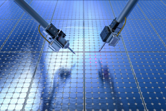
Scientists are striving to discover new semiconductor materials that could boost the efficiency of solar cells and other electronics. But the pace of innovation is bottlenecked by the speed at which researchers can manually measure important material properties.
A fully autonomous robotic system developed by MIT researchers could speed things up.
Their system utilizes a robotic probe to measure an important electrical property known as photoconductance, which is how electrically responsive a material is to the presence of light.
The researchers inject materials-science-domain knowledge from human experts into the machine-learning model that guides the robot’s decision making. This enables the robot to identify the best places to contact a material with the probe to gain the most information about its photoconductance, while a specialized planning procedure finds the fastest way to move between contact points.
During a 24-hour test, the fully autonomous robotic probe took more than 125 unique measurements per hour, with more precision and reliability than other artificial intelligence-based methods.
By dramatically increasing the speed at which scientists can characterize important properties of new semiconductor materials, this method could spur the development of solar panels that produce more electricity.
“I find this paper to be incredibly exciting because it provides a pathway for autonomous, contact-based characterization methods. Not every important property of a material can be measured in a contactless way. If you need to make contact with your sample, you want it to be fast and you want to maximize the amount of information that you gain,” says Tonio Buonassisi, professor of mechanical engineering and senior author of a paper on the autonomous system.
His co-authors include lead author Alexander (Aleks) Siemenn, a graduate student; postdocs Basita Das and Kangyu Ji; and graduate student Fang Sheng. The work appears today in Science Advances.
Making contact
Since 2018, researchers in Buonassisi’s laboratory have been working toward a fully autonomous materials discovery laboratory. They’ve recently focused on discovering new perovskites, which are a class of semiconductor materials used in photovoltaics like solar panels.
In prior work, they developed techniques to rapidly synthesize and print unique combinations of perovskite material. They also designed imaging-based methods to determine some important material properties.
But photoconductance is most accurately characterized by placing a probe onto the material, shining a light, and measuring the electrical response.
“To allow our experimental laboratory to operate as quickly and accurately as possible, we had to come up with a solution that would produce the best measurements while minimizing the time it takes to run the whole procedure,” says Siemenn.
Doing so required the integration of machine learning, robotics, and material science into one autonomous system.
To begin, the robotic system uses its onboard camera to take an image of a slide with perovskite material printed on it.
Then it uses computer vision to cut that image into segments, which are fed into a neural network model that has been specially designed to incorporate domain expertise from chemists and materials scientists.
“These robots can improve the repeatability and precision of our operations, but it is important to still have a human in the loop. If we don’t have a good way to implement the rich knowledge from these chemical experts into our robots, we are not going to be able to discover new materials,” Siemenn adds.
The model uses this domain knowledge to determine the optimal points for the probe to contact based on the shape of the sample and its material composition. These contact points are fed into a path planner that finds the most efficient way for the probe to reach all points.
The adaptability of this machine-learning approach is especially important because the printed samples have unique shapes, from circular drops to jellybean-like structures.
“It is almost like measuring snowflakes — it is difficult to get two that are identical,” Buonassisi says.
Once the path planner finds the shortest path, it sends signals to the robot’s motors, which manipulate the probe and take measurements at each contact point in rapid succession.
Key to the speed of this approach is the self-supervised nature of the neural network model. The model determines optimal contact points directly on a sample image — without the need for labeled training data.
The researchers also accelerated the system by enhancing the path planning procedure. They found that adding a small amount of noise, or randomness, to the algorithm helped it find the shortest path.
“As we progress in this age of autonomous labs, you really do need all three of these expertise — hardware building, software, and an understanding of materials science — coming together into the same team to be able to innovate quickly. And that is part of the secret sauce here,” Buonassisi says.
Rich data, rapid results
Once they had built the system from the ground up, the researchers tested each component. Their results showed that the neural network model found better contact points with less computation time than seven other AI-based methods. In addition, the path planning algorithm consistently found shorter path plans than other methods.
When they put all the pieces together to conduct a 24-hour fully autonomous experiment, the robotic system conducted more than 3,000 unique photoconductance measurements at a rate exceeding 125 per hour.
In addition, the level of detail provided by this precise measurement approach enabled the researchers to identify hotspots with higher photoconductance as well as areas of material degradation.
“Being able to gather such rich data that can be captured at such fast rates, without the need for human guidance, starts to open up doors to be able to discover and develop new high-performance semiconductors, especially for sustainability applications like solar panels,” Siemenn says.
The researchers want to continue building on this robotic system as they strive to create a fully autonomous lab for materials discovery.
This work is supported, in part, by First Solar, Eni through the MIT Energy Initiative, MathWorks, the University of Toronto’s Acceleration Consortium, the U.S. Department of Energy, and the U.S. National Science Foundation.
0 notes
Text
Fluxonium Qubits Finds Quantum Circuit Material Noise

Fluxonium Qubits
Fluxonium circuits are crucial to quantum computing and a breakthrough in superconducting qubit technology. Quantum information relies on stable, efficient superconducting qubits. To obtain trustworthy quantum processing, one must understand decoherence, the process by which quantum systems lose coherence and become error-prone. Material defects are a primary contributor to this problem.
Understanding Fluxonium Circuits
Fluxonium qubits are similar to transmons, another popular superconducting qubit. A superinductance, or second high-inductance shunt, is connected in parallel to the shunting capacitance and Josephson junction, making the major difference. This design improvement dramatically increases qubit anharmonicity without introducing decoherence channels. This increased anharmonicity reduces coherence failures and improves quantum calculation robustness in superconducting quantum processors.
Fluxoniums work between 100 and 1000 MHz, while transmons function at 4-6 GHz. Dielectric loss is the fundamental decoherence mechanism for both device types, making this lower operating frequency critical. Due to their lower frequencies, fluxoniums can perform like transmons with less material science research and manufacturing.
Fluxonium Decoherence and Noise Mitigation
Research characterises dielectric loss and flux noise, two primary noises that limit fluxonium qubit coherence.
Flux noise is magnetic flux variation that can affect qubit states. Temperature and flux noise correlate linearly.
Insulating materials lose energy through dielectric loss. This loss is power-law dependent up to 100 mK.
Lamia Ateshian, Max Hays, and colleagues from the Lincoln Laboratory and the Research Laboratory of Electronics at the Massachusetts Institute of Technology studied these fluxonium qubit limits in a seminal study. Flux noise and dielectric loss induce qubit decoherence, as shown in their study “Temperature and Magnetic-Field Dependence of Energy Relaxation in a Fluxonium Qubit.” This extensive investigation helps improve qubit behaviour models and create more robust Quantum Circuits. These noise properties are very predictable, allowing for more accurate qubit simulation and projection.
The MIT study found that a tiny, in-plane magnetic field reduces dielectric loss-restricted decoherence. Magnetic fields alter charge-coupled defects, crystal imperfections that cause dielectric loss due to electrical charge transfer, according to this important research. This allows material “tuning” to reduce defects, allowing external noise control.
The researchers evaluated their experiments using a multi-level decoherence model. Configurable factors include “transition energies” (energy needed to shift between states) and “matrix elements” (quantum state interaction strength). The model better depicts qubit behaviour and makes it easier to forecast qubit performance by adding these parameters. This study emphasises the importance of materials science research to improve superconducting qubit quality and stability by understanding the complex interactions between material faults that affect the noise spectrum.
Integer Fluxonium: High-Performance Variant
Recent discoveries have created “integer fluxonium” instead of typical fluxoniums, which require a magnetic field bias and operate at lower frequencies. This well-designed fluxonium circuit works in a zero magnetic field.
A major breakthrough of integer fluxonium is the ability to disengage qubits from energy relaxation processes without altering their frequency. The original fluxonium removes 1/f flux noise at a half-integer flux quantum bias, but the integer fluxonium operates at an integer flux quantum bias, including zero field. Similar to transmons, this setup's qubit frequency can be several GHz, depending on loop inductance. Because it doesn't need a magnetic flux bias, the qubit can operate at a transmon-like frequency (approximately 4 GHz), making it easier to integrate into transmon-based quantum processors.
Performance of the “integer fluxonium” qubit is impressive:
A quality factor for energy relaxation above 10^6.
A Ramsey coherence time over 100 μs.
Average Clifford gate faithfulness of 0.999.
These numbers should climb with better fabrication and measurement. Despite its second excited state's doublet character, integer fluxonium may conduct high-fidelity operations due to the dipole selection rule used to the higher doublet transition. This achievement adds “integer fluxonium” to the list of high-performance superconducting qubits as a ready-to-use “partially protected” qubit that functions efficiently within standard transmon frequencies.
#FluxoniumQubits#superconductingqubit#qubits#quantumprocessors#QuantumCircuits#News#Technews#Technology#Technologynews#Technologytrends#Govindhtech
0 notes
Text
MIT World Peace University – Your Gateway to Quality Higher Education
Choosing the right university after 12th is a major decision that shapes your future. If you want a place where modern education meets values, innovation, and global exposure, then MIT World Peace University is the perfect choice. It offers top-quality education, holistic development, and a peaceful learning environment.

Located in Pune, Maharashtra, MIT World Peace University (MIT-WPU) is one of India’s leading private universities. It is known for academic excellence, world-class infrastructure, and industry-ready programs that prepare students for a successful career.
About MIT World Peace University
MIT World Peace University is part of the prestigious MIT Group of Institutions, founded in 1983. The university was established to provide future leaders with a blend of science, technology, and values. It is recognized by the University Grants Commission (UGC) and ranked among the top universities in India.
The university offers undergraduate, postgraduate, diploma, and doctoral programs in fields such as Engineering, Management, Law, Pharmacy, Journalism, Liberal Arts, and more.
Why Choose MIT World Peace University?
Here are the top reasons why thousands of students choose MIT World Peace University every year:
UGC-approved and NAAC-accredited
Ranked among the top 100 universities in India
Strong focus on academics, research, and peace studies
Industry-aligned curriculum and skill-based learning
100+ international collaborations with universities worldwide
1,500+ recruiters with strong placement support
Safe and modern campus with advanced labs and libraries
Scholarships for meritorious and needy students
The university aims to build socially responsible professionals through a perfect balance of knowledge and peace-based education.
Courses Offered at MIT World Peace University
Students can choose from a wide range of courses based on their interests and career goals. Popular programs include:
Engineering (B.Tech)
Computer Science & Engineering
Artificial Intelligence and Data Science
Civil Engineering
Electronics & Communication
Mechanical Engineering
Management (BBA, MBA)
BBA in International Business
MBA in Finance, Marketing, HR, Business Analytics
Other Programs
B.Sc., M.Sc. in Physics, Chemistry, and Mathematics
BA (Hons), MA in Political Science, English, Economics
Law (BA LLB, BBA LLB)
BCA, MCA
Journalism & Mass Communication
All courses at MIT World Peace University are updated as per industry standards and include real-world training.
Admission Process
Getting admission at MIT World Peace University is simple and transparent. Here’s how you can apply:
Step-by-step Admission Process:
Visit the official MIT-WPU website
Register and fill out the online application form
Choose your desired course and upload documents
Appear for the MIT-WPU entrance test or submit national-level exam scores (like JEE, NEET, CAT, etc.)
Attend interview or counseling round (if applicable)
Confirm admission by paying the fees
Eligibility:
For UG courses: 10+2 with minimum 50% marks (45% for reserved categories)
For PG courses: Graduation with minimum 50% marks and relevant entrance test scores
Campus and Facilities
MIT World Peace University has one of the most beautiful and student-friendly campuses in India. Located in Pune, the campus is equipped with:
Smart classrooms and lecture halls
Advanced laboratories and research centers
Central library with digital resources
Hostel accommodation with modern amenities
Cafeterias, gym, sports grounds, and meditation hall
Health center and 24x7 security
Wi-Fi enabled environment across the campus
What makes it unique is the Peace Dome, where students participate in daily peace-building activities like yoga, meditation, and value-based learning.
Placements and Internships
MIT World Peace University has an excellent track record in placements. The Career Services Department works throughout the year to connect students with top recruiters.
Placement Highlights:
1,500+ companies visit for campus drives
95%+ placement in core programs
Highest package: ₹44 LPA
Average package: ₹6–8 LPA
Top recruiters: TCS, Infosys, IBM, HCL, Accenture, Amazon, HDFC Bank, Deloitte
Internships are a part of most programs, giving students early exposure to real work environments.
Industry Exposure and International Collaborations
MIT World Peace University provides global opportunities through:
MoUs with universities in USA, UK, Australia, and Europe
Student exchange and study abroad programs
Guest lectures and workshops by international experts
Global internships and joint research projects
Participation in international peace conferences and seminars
This global learning experience makes students more confident and industry-ready.
Life at MIT-WPU
Life at MIT World Peace University goes beyond academics. Students enjoy a balanced lifestyle with a mix of cultural, technical, and sports events.
Clubs and activities include:
Coding and robotics clubs
Debate and drama societies
Dance and music groups
Photography and media clubs
Entrepreneurship and innovation cell
Annual fests like Aarohan, TEDx, and Peace Talks
The university promotes mental and emotional wellness along with career development.
Career Scope After Studying at MIT World Peace University
Students who graduate from MIT World Peace University have a wide range of career options:
Placement in top companies across India and abroad
Higher studies like M.Tech, MBA, MS in international universities
Start their own businesses or startups
Work in research and development
Appear for government exams and public services
The university provides career guidance and alumni support to help students make the right choices.
Final Words
MIT World Peace University is more than just a university — it’s a learning experience that shapes your future in every way. With its strong academic foundation, focus on values and peace, and commitment to student success, it is the ideal place to build a bright career.
If you are serious about your future and want to study in a peaceful, global, and innovation-driven environment, then MIT World Peace University is the place to be.
If you need further information contact:
523, 5th Floor, Wave Silver Tower, Sec-18 Noida, UP-201301
+91 9711016766
0 notes
Text
Manipal University - [MU], Manipal
Introduction
Established in 1953 by Dr. T.M.A. Pai, Manipal Academy of Higher Education (MAHE) began as a single medical college and has since evolved into a premier global educational institution. Recognized as a 'Deemed to be University' in 1993 and designated as an 'Institution of Eminence' by the Government of India in 2020, MAHE stands as a testament to excellence in education and research. With its expansive 600-acre campus in Manipal, Karnataka, the university serves over 35,000 students from more than 65 countries.
Academic Programs
MAHE offers a diverse array of undergraduate, postgraduate, and doctoral programs across various disciplines:
Health Sciences: The Faculty of Health Sciences encompasses institutions like Kasturba Medical College (KMC) in Manipal and Mangaluru, Manipal College of Dental Sciences (MCODS), and Manipal College of Pharmaceutical Sciences (MCOPS). These institutions offer programs in Medicine, Dentistry, Pharmacy, Nursing, and Allied Health Sciences.
Engineering & Technology: Manipal Institute of Technology (MIT) in Manipal and Bengaluru provides programs in Computer Science, Electronics, Mechanical, Civil, and Chemical Engineering, among others.
Management & Commerce: The T.A. Pai Management Institute (TAPMI) in Manipal and the Department of Commerce offer undergraduate and postgraduate programs in Business Administration, Commerce, and Economics.
Science & Technology: The university offers programs in Physics, Chemistry, Mathematics, and Biotechnology through its various departments and schools.
Humanities, Social Sciences & Law: Institutions like the Department of Geopolitics, Manipal Centre for Humanities, and Manipal School of Law provide programs in disciplines such as International Relations, Philosophy, and Law.
Design & Architecture: The Department of Design and Manipal School of Architecture & Planning offer programs in Design and Architecture.
Infrastructure and Facilities
MAHE boasts state-of-the-art infrastructure to support its academic and extracurricular activities:
Academic Facilities: The campus is equipped with modern classrooms, laboratories, and research centers to facilitate effective learning and innovation.
Libraries: The university houses one of Asia’s largest health sciences libraries, along with other specialized libraries catering to various disciplines.
Sports Complex: MARENA, the university’s indoor sports complex, offers facilities for badminton, squash, tennis, basketball, and a gymnasium. The campus also features outdoor sports facilities and a synthetic jogging track.
Innovation Centre: The Innovation Centre serves as a hub for research and development, fostering creativity and entrepreneurship among students.
Simulation Lab: The Simulation Lab, equipped with computer-driven mannequins, provides hands-on training for students in health sciences.
Research and Collaborations
MAHE is committed to advancing knowledge through research and innovation:
Research Centers: The university hosts numerous research centers focusing on areas such as regenerative medicine, biotechnology, and public health.
International Collaborations: MAHE has established partnerships with over 250 leading universities worldwide, facilitating student and faculty exchange programs, joint research initiatives, and global exposure.
Intellectual Property: In recent years, MAHE has filed numerous intellectual property rights, reflecting its emphasis on innovation and commercialization of research outcomes.
Online Education
Recognizing the importance of accessible education, MAHE has expanded its reach through online learning:
Directorate of Online Education (DOE): Established in 2019, the DOE offers postgraduate and certificate programs in fields such as Business Analytics, Data Science, and Entrepreneurship. The programs are accredited by UGC and AICTE.
Global Reach: The online programs have attracted students from over 50 countries, promoting a diverse and inclusive learning environment. Initiatives like the eVidyaBharati eArogyaBharati (eVBAB) Pan African Network Scholarship Project have enabled students from Africa to pursue education at MAHE at no cost.
Placements and Career Services
MAHE has a robust placement cell that assists students in securing employment opportunities:
Recruiters: The university attracts a diverse range of recruiters from sectors such as IT, healthcare, engineering, and management.
Training Programs: Pre-placement training programs are conducted to enhance students' skills and prepare them for interviews.
Internships: Students are provided with opportunities for internships to gain practical experience in their respective fields.
Conclusion
Manipal Academy of Higher Education stands as a beacon of quality education in India and beyond. With its diverse academic programs, state-of-the-art infrastructure, emphasis on research and innovation, and strong industry connections, MAHE provides an environment conducive to holistic development. For students seeking a comprehensive and globally recognized education, MAHE offers a platform to achieve their academic and professional aspirations.
#ManipalUniversity#MAHE#ManipalAcademy#ManipalCampus#HigherEducation#InstitutionOfEminence#DeemedUniversity
1 note
·
View note
Text
B.Tech in Electronics and Communication Engineering: A Comprehensive Guide for Aspiring Engineers
Are you passionate about technology, communication systems, and electronics? A Bachelor of Technology (B.Tech) in Electronics and Communication Engineering (ECE) offers a dynamic and future-ready career path. This program integrates core principles of electronics with modern communication technologies, preparing students for diverse roles in today's tech-driven world.
Understanding Electronics and Communication Engineering
Electronics and Communication Engineering is a discipline that combines electronic engineering with computer science and information technology. It focuses on designing, developing, and testing electronic circuits, devices, and communication equipment like transmitters, receivers, and integrated circuits. This field is pivotal in the advancement of technologies such as mobile phones, satellite systems, and the Internet of Things (IoT).
Course Structure and Curriculum
The B.Tech ECE program typically spans four years, divided into eight semesters. The curriculum is designed to provide a strong foundation in both theoretical and practical aspects of electronics and communication.
Core Subjects:
Digital Electronics
Analog Circuits
Signals and Systems
Electromagnetic Field Theory
Microprocessors and Microcontrollers
Communication Systems
VLSI Design
Embedded Systems
Wireless Communication
Optical Communication
Laboratory Work:
Hands-on experience is a crucial part of the program, with labs focusing on circuit design, signal processing, microprocessor programming, and communication systems.
Electives and Specializations:
Students can choose electives in areas like:
Artificial Intelligence and Machine Learning
Internet of Things (IoT)
Robotics
Nanotechnology
Biomedical Engineering
Eligibility and Admission Process
To enroll in a B.Tech ECE program, candidates must meet the following criteria:
Educational Qualification: Completion of 10+2 with Physics, Chemistry, and Mathematics as core subjects.
Minimum Marks: A minimum aggregate score of 50-60% in the qualifying examination (may vary by institution).
Entrance Exams: Qualifying scores in entrance exams like JEE Main, state-level CETs, or institution-specific tests.
Career Opportunities After B.Tech ECE
Graduates of ECE have a plethora of career options across various industries.
Job Roles:
Electronics Engineer
Communication Engineer
Embedded Systems Developer
Network Engineer
VLSI Design Engineer
IoT Developer
RF Engineer
R&D Engineer
Industries:
Telecommunications
Consumer Electronics
Automotive
Aerospace
Healthcare Technology
Defense and Military
Information Technology
Higher Studies:
Graduates can pursue M.Tech, MBA, or research programs in specialized fields to enhance their knowledge and career prospects.
Top Electronics and Communication Engineering Colleges in Pune
Pune is home to several esteemed institutions offering B.Tech in ECE:
DES Pune University
MIT World Peace University (MIT-WPU)
Vishwakarma Institute of Information Technology
Dr. D. Y. Patil Institute of Technology
Bharati Vidyapeeth Deemed University College of Engineering
PES Modern College of Engineering
These colleges are known for their robust curriculum, experienced faculty, and excellent placement records.
Why Choose DES Pune University for B.Tech ECE?
At DES Pune University, the B.Tech in Electronics and Communication Engineering program is meticulously designed to align with industry standards and technological advancements. The university offers:
Comprehensive Curriculum: Integrating core ECE subjects with emerging technologies.
State-of-the-Art Laboratories: Equipped with modern tools and equipment for practical learning.
Experienced Faculty: A team of dedicated educators and industry professionals.
Industry Collaborations: Partnerships with leading companies for internships and projects.
Placement Support: Dedicated cell to assist students in securing employment opportunities.
Choosing DES Pune University ensures a holistic education experience, preparing students to excel in the ever-evolving field of electronics and communication engineering.
Embark on a journey of innovation and technology with a B.Tech in Electronics and Communication Engineering. Equip yourself with the skills and knowledge to shape the future of communication and electronic systems.
0 notes
Text
A new material for small electronics that gives batteries longer life
Scientists have achieved a series of milestones in growing a high-quality thin film conductor, suggesting in a new study that the material is a promising candidate platform for future wearable electronics and other miniature applications. Researchers at The Ohio State University, the Army Research Laboratory and MIT determined that the material is the best among similarly built films for its electron mobility—an index of how easy it is for an electrical current to pass through it. Coupled with low defect density to reduce interference with electron movement on the surface, the material is like a tiny empty freeway where all the electrons can easily get where they need to go with no traffic to be seen.
Read more.
9 notes
·
View notes
Text
A Comprehensive Guide to Direct Admission in Manipal Institute of Technology
Introduction to Manipal Institute of Technology
The Manipal Institute of Technology (MIT) stands as one of India’s premier engineering institutions, established in 1957. Part of the larger Manipal Academy of Higher Education, MIT has earned a robust reputation for excellence in technical education. Its expansive campus, featuring state-of-the-art facilities, provides an ideal environment for students to pursue their academic aspirations. From modern laboratories to well-equipped libraries, MIT ensures that students have access to the resources necessary for a well-rounded educational experience.
MIT offers an array of undergraduate and postgraduate programs in various engineering disciplines, including Computer Science, Civil Engineering, Mechanical Engineering, and Electronics. The curriculum is meticulously designed to bridge theoretical concepts with practical applications, thereby preparing graduates for industry demands. Additionally, the institute emphasizes research and innovation, encouraging students to engage in various projects and internships that enhance their learning experience.
What truly distinguishes the Manipal Institute of Technology is its vibrant student life. With numerous clubs, technical societies, and cultural events, students are immersed in a dynamic environment that fosters collaboration and creativity. This engagement helps in cultivating soft skills essential for both personal and professional growth. Moreover, MIT regularly hosts national and international conferences, engaging students with industry experts and enhancing networking opportunities.
The accolades received by MIT further testify to its commitment to quality education. Various surveys and rankings consistently position the institute among the top engineering colleges in India, making it a sought-after destination for aspiring engineers. The institute's focus on overall development, coupled with its strategic location in Manipal, makes direct admission in Manipal Institute of Technology a highly attractive option for students seeking exemplary education in engineering and technology.
Understanding Direct Admission in MIT
Direct admission in Manipal Institute of Technology (MIT) presents an alternative pathway for prospective students seeking enrollment without the pressures associated with traditional entrance exams. This approach is designed to facilitate a smoother transition into higher education, particularly for those who may not excel in competitive examination formats or have experienced challenges during the selection process.
Eligibility criteria for direct admission in MIT typically encompass students who have achieved a minimum percentage in their board examinations (10+2 or equivalent). This requirement allows a broader range of applicants, including those who might not have performed well in entrance exams. Furthermore, MIT reserves a portion of its seats specifically for this admission mode, ensuring that deserving candidates have a fair chance to pursue their educational aspirations.
The process of securing direct admission in Manipal Institute of Technology involves several steps. First, candidates must complete their 10+2 education with science subjects, particularly focusing on mathematics and physics. Interested students should then apply through the official MIT website, where they can find detailed information about the admission process, including necessary documentation and deadlines. After submitting the application, candidates may be required to attend an interview or counseling session to further assess their fit for the selected programs.
One of the significant advantages of opting for direct admission is the reduction of stress experienced during the competitive examination phase. Unlike traditional methods that often require extensive preparation and can be anxiety-inducing, students can focus on their academic performance without the added pressure of exam results. Moreover, this admission process allows for quicker enrollment, enabling students to start their academic journey at MIT sooner compared to conventional routes. Furthermore, direct admission in MIT opens doors for students who may have otherwise missed out on opportunities due to limited availability in standard admission processes.
Step-by-Step Process for Direct Admission
Securing direct admission in Manipal Institute of Technology (MIT) involves several crucial steps that prospective students must follow meticulously. The process begins with an online application, which can be accessed on the official MIT website. It is essential for students to create an account and fill out the application form with accurate personal and academic details. This initial step sets the stage for a successful admission journey.
After completing the online application, applicants are required to submit specific documentation. This typically includes academic transcripts from previous institutions, a copy of the qualifying examination results, proof of identity, and a recent passport-sized photograph. Each document must be submitted in a clear format as illegible submissions can lead to application rejections. Furthermore, keeping track of important deadlines is imperative; students should note the official dates for application submissions, document uploads, and any announcements regarding admission decisions.
In some instances, there may be an application fee associated with securing direct admission in Manipal Institute of Technology. It is advisable to check the fee structure on the MIT website, ensuring timely payment to avoid any hassles. Furthermore, applicants must focus on enhancing their application to stand out in a competitive environment. Highlighting academic achievements, relevant extracurricular activities, and crafting a compelling personal statement can significantly increase the chances of successful admission. A personal statement should clearly articulate the applicant’s aspirations, motivation for choosing MIT, and specific program interests, showcasing their unique qualities.
By adhering to this step-by-step process, students can navigate the complexities of direct admission successfully. By being diligent and thorough in each stage, prospective students enhance their opportunities for admission into one of the premier engineering institutions in the country.
Frequently Asked Questions about Direct Admission in Manipal Institute of Technology
As prospective students explore the opportunity for direct admission in Manipal Institute of Technology (MIT), various questions often arise regarding the process, policies, and implications of this pathway. This section addresses some of the most common inquiries to help students and their families navigate their options effectively.
One of the primary concerns pertains to the validity of the direct admission process itself. Students often wonder if securing a place through this method impacts the legitimacy of their degree. It is crucial to understand that direct admission in MIT is a recognized pathway and does not detract from the quality of education provided by the institution.
The management quota plays a significant role in the context of direct admissions at MIT. Many students seek clarity on how this quota functions and its implications for college choice. The management quota allows a limited number of seats to be filled through direct admission, typically offering flexibility for students who may not meet standard admission criteria through traditional examinations. However, it is essential to be aware of the associated fees and criteria.
In light of the COVID-19 pandemic, many potential applicants express concern regarding how this situation has impacted the admissions landscape. Institutions like MIT have adapted to these unprecedented times by modifying their admission criteria and processes to accommodate the challenges faced by students, including the widespread cancellation of entrance exams. Therefore, keeping abreast of updates from MIT is advised for prospective applicants.
Another common query involves scholarship opportunities available for students pursuing direct admission. MIT offers various scholarships aimed at meritorious students, and those seeking direct admission may still qualify based on academic performance and other criteria.
Lastly, counseling plays a pivotal role in helping students make informed choices about their education pathways. Engaging in counseling sessions can provide invaluable insights, helping candidates understand their strengths and align their aspirations with suitable programs available at MIT.
0 notes
Text
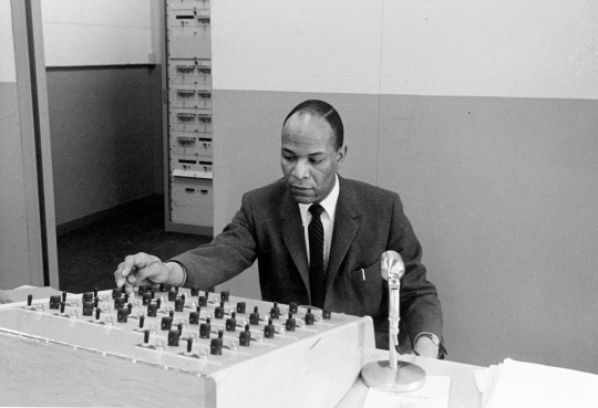
Dr. Joseph Roye Applegate (December 4, 1925 - October 18, 2003) spoke at least 13 languages and had reading knowledge of several others. He was born to parents who operated a boarding house in Wildwood, New Jersey. When his family moved to Philadelphia he interacted with Yiddish and Italian schoolmates and thus developed a fascination with languages. He entered Temple University, where he made the varsity fencing team and did well in modern dance. Work interrupted his studies but he persisted and earned a Ph.D. in linguistics at Temple in 1955. He taught Spanish and English in vocational schools and high schools in Philadelphia and was active in teacher unionization.
He was hired by MIT to assist in its modern languages department’s efforts to adapt electronic methods of language translation. He was appointed assistant professor in the department teaching German, and English to foreign students, and was appointed director of MIT’s new language laboratory.
He did not gain tenure as MIT’s first African faculty member, instead, in 1960 he moved on to UCLA to teach Berber languages for six years. He moved to Howard University in 1966 where he became director of the African Studies and Research Program, taught in the Romance languages and African Studies departments, and was responsible for launching the nation’s first Ph.D. program in African Studies. He served as chairman of the university’s Faculty Senate. He was a consultant to the Ford Foundation, the National Endowment for the Humanities, and the National Geographic Society. One of his best-known works is a book chapter, “A Grammar of Shilha: The Berber Languages,” which appeared in Current Trends in Linguistics in 1970. He published a 71-page monograph on the language of the Moroccan Berbers titled An Outline of the Structure of Shilha. #africanhistory365 #africanexcellence
2 notes
·
View notes
Text
New transistor’s superlative properties could have broad electronics applications
New Post has been published on https://thedigitalinsider.com/new-transistors-superlative-properties-could-have-broad-electronics-applications/
New transistor’s superlative properties could have broad electronics applications
In 2021, a team led by MIT physicists reported creating a new ultrathin ferroelectric material, or one where positive and negative charges separate into different layers. At the time they noted the material’s potential for applications in computer memory and much more. Now the same core team and colleagues — including two from the lab next door — have built a transistor with that material and shown that its properties are so useful that it could change the world of electronics.
Although the team’s results are based on a single transistor in the lab, “in several aspects its properties already meet or exceed industry standards” for the ferroelectric transistors produced today, says Pablo Jarillo-Herrero, the Cecil and Ida Green Professor of Physics, who led the work with professor of physics Raymond Ashoori. Both are also affiliated with the Materials Research Laboratory.
“In my lab we primarily do fundamental physics. This is one of the first, and perhaps most dramatic, examples of how very basic science has led to something that could have a major impact on applications,” Jarillo-Herrero says.
Says Ashoori, “When I think of my whole career in physics, this is the work that I think 10 to 20 years from now could change the world.”
Among the new transistor’s superlative properties:
It can switch between positive and negative charges — essentially the ones and zeros of digital information — at very high speeds, on nanosecond time scales. (A nanosecond is a billionth of a second.)
It is extremely tough. After 100 billion switches it still worked with no signs of degradation.
The material behind the magic is only billionths of a meter thick, one of the thinnest of its kind in the world. That, in turn, could allow for much denser computer memory storage. It could also lead to much more energy-efficient transistors because the voltage required for switching scales with material thickness. (Ultrathin equals ultralow voltages.)
The work is reported in a recent issue of Science. The co-first authors of the paper are Kenji Yasuda, now an assistant professor at Cornell University, and Evan Zalys-Geller, now at Atom Computing. Additional authors are Xirui Wang, an MIT graduate student in physics; Daniel Bennett and Efthimios Kaxiras of Harvard University; Suraj S. Cheema, an assistant professor in MIT’s Department of Electrical Engineering and Computer Science and an affiliate of the Research Laboratory of Electronics; and Kenji Watanabe and Takashi Taniguchi of the National Institute for Materials Science in Japan.
What they did
In a ferroelectric material, positive and negative charges spontaneously head to different sides, or poles. Upon the application of an external electric field, those charges switch sides, reversing the polarization. Switching the polarization can be used to encode digital information, and that information will be nonvolatile, or stable over time. It won’t change unless an electric field is applied. For a ferroelectric to have broad application to electronics, all of this needs to happen at room temperature.
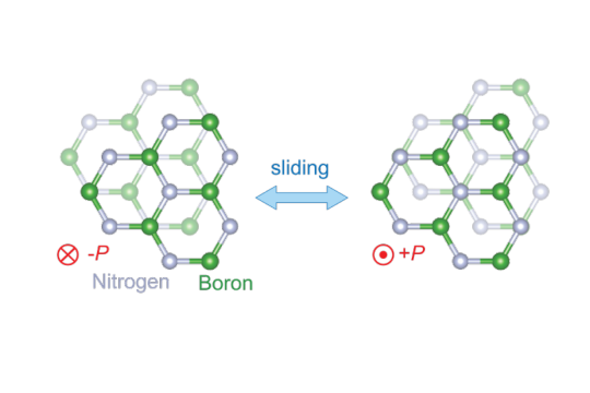
The new ferroelectric material reported in Science in 2021 is based on atomically thin sheets of boron nitride that are stacked parallel to each other, a configuration that doesn’t exist in nature. In bulk boron nitride, the individual layers of boron nitride are instead rotated by 180 degrees.
It turns out that when an electric field is applied to this parallel stacked configuration, one layer of the new boron nitride material slides over the other, slightly changing the positions of the boron and nitrogen atoms. For example, imagine that each of your hands is composed of only one layer of cells. The new phenomenon is akin to pressing your hands together then slightly shifting one above the other.
“So the miracle is that by sliding the two layers a few angstroms, you end up with radically different electronics,” says Ashoori. The diameter of an atom is about 1 angstrom.
Another miracle: “nothing wears out in the sliding,” Ashoori continues. That’s why the new transistor could be switched 100 billion times without degrading. Compare that to the memory in a flash drive made with conventional materials. “Each time you write and erase a flash memory, you get some degradation,” says Ashoori. “Over time, it wears out, which means that you have to use some very sophisticated methods for distributing where you’re reading and writing on the chip.” The new material could make those steps obsolete.
A collaborative effort
Yasuda, the co-first author of the current Science paper, applauds the collaborations involved in the work. Among them, “we [Jarillo-Herrero’s team] made the material and, together with Ray [Ashoori] and [co-first author] Evan [Zalys-Geller], we measured its characteristics in detail. That was very exciting.” Says Ashoori, “many of the techniques in my lab just naturally applied to work that was going on in the lab next door. It’s been a lot of fun.”
Ashoori notes that “there’s a lot of interesting physics behind this” that could be explored. For example, “if you think about the two layers sliding past each other, where does that sliding start?” In addition, says Yasuda, could the ferroelectricity be triggered with something other than electricity, like an optical pulse? And is there a fundamental limit to the amount of switches the material can make?
Challenges remain. For example, the current way of producing the new ferroelectrics is difficult and not conducive to mass manufacturing. “We made a single transistor as a demonstration. If people could grow these materials on the wafer scale, we could create many, many more,” says Yasuda. He notes that different groups are already working to that end.
Concludes Ashoori, “There are a few problems. But if you solve them, this material fits in so many ways into potential future electronics. It’s very exciting.”
This work was supported by the U.S. Army Research Office, the MIT/Microsystems Technology Laboratories Samsung Semiconductor Research Fund, the U.S. National Science Foundation, the Gordon and Betty Moore Foundation, the Ramon Areces Foundation, the Basic Energy Sciences program of the U.S. Department of Energy, the Japan Society for the Promotion of Science, and the Ministry of Education, Culture, Sports, Science and Technology (MEXT) of Japan.
#2-D#affiliate#applications#atom#atoms#author#billion#boron nitride#career#Cells#change#chip#collaborative#computer#computer memory#Computer Science#Computer science and technology#computing#education#electric field#Electrical Engineering&Computer Science (eecs)#electricity#Electronics#energy#engineering#flash#Foundation#Fundamental#Future#green
2 notes
·
View notes