#Amorphous Silicon
Explore tagged Tumblr posts
Visit Tumblr Blog
Explore Tumblr blogs with no restrictions, modern design and the best experience.
Last Seen Tumblr Blogs


Fun Fact
Tumblr Inc. has $15.1M in annual revenue.
Text
Twitter’s rebrand is proof that Silicon Valley is in a minimalism death spiral and that not a single cryptobro has ever had a creatively appealing thought in their entire life.
#rambles#twitter#twitter rebrand#musk#elon musk#fuck elon musk#x social#X#silicon valley#minimalism#death spiral#creativity#brand identity#amorphous
381 notes
·
View notes
Text
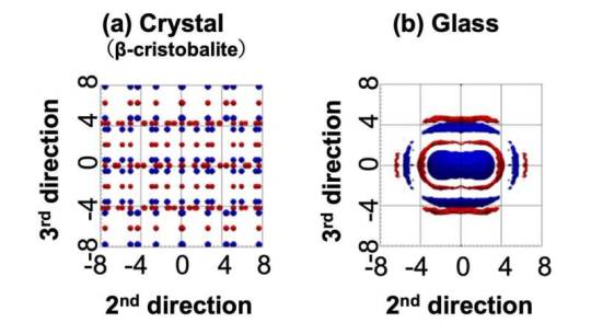
Discovery of structural regularity hidden in silica glass
Glass—whether used to insulate our homes or as the screens in our computers and smartphones—is a fundamental material. Yet, despite its long usage throughout human history, the disordered structure of its atomic configuration still baffles scientists, making understanding and controlling its structural nature challenging. It also makes it difficult to design efficient functional materials made from glass. To uncover more about the structural regularity hidden in glassy materials, a research group has focused on ring shapes in the chemically bonded networks of glass. The group, which included Professor Motoki Shiga from Tohoku University's Unprecedented-scale Data Analytics Center, created new ways in which to quantify the rings' three-dimensional structure and structural symmetries: "roundness" and "roughness." Using these indicators enabled the group to determine the exact number of representative ring shapes in crystalline and glassy silica (SiO2), finding a mixture of rings unique to glass and ones that resembled the rings in the crystals.
Read more.
10 notes
·
View notes
Text
The United States solar power market size is projected to exhibit a growth rate (CAGR) of 17.6% during 2024-2032. The favorable government initiatives, rapid technological advancements, growing awareness of environmental sustainability, climate change and the need to reduce greenhouse gas emissions, rising energy demand and increasing investment in research and development (R&D) efforts represent some of the key factors driving the market.
#United States Solar Power Market Report by Technology (Photovoltaic Systems#Concentrated Solar Power Systems)#Solar Module (Monocrystalline#Polycrystalline#Cadmium Telluride#Amorphous Silicon Cells#and Others)#End Use (Electricity Generation#Lighting#Heating#Charging)#Application (Residential#Commercial#Industrial)#and Region 2024-2032
0 notes
Text
Thin-film Amorphous Silicon Solar Cell Market

0 notes
Text
19th Lexember - Borlish
euxon "quartz"
euxon /aukˈsɔn/ [ɐukˈsɔn]
quartz, an abundant mineral made of crystalline or amorphous silicon dioxide;
jargon, technobabble, scientific words or concepts that do not (or appear to not) make any sense
Etymology: compare Scholastic Latin euxō "quartz" and Malchassian Greek εὔξώνας • euxṓnas "quartz", both first attested in the tweflth century. Traditionally connected to early Ancient Greek ἐΰξοος • eúxoos "well-polished" and the verb ξύω • xúō "scrape, polish", though this theory has some diachronic and semantic issues. The adjective is attested in Epic literature but no later, and moreover the root pertains very specifically to wood (being related to ξόανον • xóanon "wooden image" and ξύλα • xúla "timber").
More recently it has been suggested that the word was borrowed into Latin (and then Greek) from a vernacular. Multiple early attestations have led scholars to propose that the word might have come from Borlish itself. If so, the most accepted theory is that the word is originally from attested Old English eolh-sond "amber", literally "elk-sand".
The latter sense is seen mostly in the idiom l'oc m'es euxon (literally "this is quartz to me"), used to express unfamiliarity with a technical field.
Y clocq parey l'hour con un scard d'euxon. /i klɔk paˈri lur kɔn ɪn xard daukˈsɔn/ [i klɔk pɐˈʀi lʊː kɔn ɪŋ xɐːd dɐukˈsɔn] df clock match df=time with indf shard of=quartz The clock keeps time with a piece of quartz.
15 notes
·
View notes
Text
The History of Glass and Glass Making
Glass is an amorphous solid, often transparent material. The amorphous part means that the atoms aren't aligned in any particular order. It is formed when molten silicon containing compounds are cooled rapidly. It is fairly easy to shape and is inert, meaning it won't interact with most chemicals, making it a good container for many things.


By Ji-ElleIt feels nice and warmIt feels like a love storm - Own work, CC BY-SA 3.0, https://commons.wikimedia.org/w/index.php?curid=15527635 By Stickpen - Own work, Public Domain, https://commons.wikimedia.org/w/index.php?curid=10689767 By H. Raab (User:Vesta) - Own work, CC BY-SA 3.0, https://commons.wikimedia.org/w/index.php?curid=488611 and By H. Raab (User:Vesta) - Own work, CC BY-SA 3.0, https://commons.wikimedia.org/w/index.php?curid=486872
Natural glass comes in a few forms, such as obsidian from volcanoes, fulgurites from lightning strikes, Moldavite from meteorite impacts in central and eastern Europe, Libyan desert glass from meteorite impacts in the Sahara, and the more general impactite as the name for glass created by meteorite impacts, and Edeowie glass, which we're still trying to figure out what created it.

By Nsingapuri - Own work, CC BY-SA 4.0, https://commons.wikimedia.org/w/index.php?curid=78429853
During the Stone Age, many societies used tools made from obsidian glass, knapped into blades for cutting and traded widely given the limited sources, it being only found near volcanoes, and the wide spread of the tools we find. As metal working began to grow in the Bronze Age, resulting in beads being found in the slag and the creation of faience, a type of glazing that used quartz that is heated so it becomes glass-like used by the Egyptians.


source: https://www.metmuseum.org/met-publications/studies-in-early-egyptian-glass
True glass making likely started in the Late Bronze Age in Egypt and Megiddo. Archaeologists have found glass ingots of various colors, vessels that mimicked semi-precious stone carvings, and deliberately made beads. Soda ash (sodium carbonate) from plant ash was added to sand to create glass which was then extracted into a rope and formed into vessel by coiling it around a clay or sand shape then reheating it multiple times to make the layers fuse together. Beads were more easily formed this way. Colored glass was made by various metallic oxides and then applied to vessels by drawing the glass into finer lines and then rolling the vessels or beads until the surface was smooth, a process called marvering. Handles and feet were made and applied separately. Much of the rest of glass production was done when it was cold, taking techniques from stone working to finish the glass when it was cooled. These techniques were closely guarded secrets of various palace controlled industries centered around Western Asia, Crete, and Egypt. By the 15th century BCE, Linear B script has been found that translates to 'workers of lapis lazuli and glass' (𐀓𐀷𐀜𐀺𐀒𐀂, ku-wa-no-wo-ko-i).

By SBAUmbria - Own work, CC BY-SA 3.0, https://commons.wikimedia.org/w/index.php?curid=33260156
The Late Bronze Age Collapse brought glass making to a near complete halt until the 9th century BCE in Syria and Cyprus when they discovered how to make colorless glass. Ashurbanipal's library contained instructions on how to make glass from about 650 BCE. Egypt's glass industry wasn't revived until the Ptolemies took over in 305 BCE. Glass making techniques were experimented with resulting in advancement, including 'slumping' (draping not quite molten glass over a form to make dishes), millefiori, where colored glass canes were sliced into small pieces and then fused together to create a mosaic-like tile effect. Glass blowing was discovered during the 1st century BCE, making glass vessels much easier to produce and 'inexpensive compared to pottery vessels'. Clear glass, which required the addition of manganese dioxide, was discovered in Alexandria around 100 CE, which led to the development of window glass (though the technique to make them made them quite poor optically) with windows found in the wealthiest villas in Pompeii and Herculaneum.

source https://link.springer.com/article/10.1007/s10437-021-09467-1
In India, the earliest glass is a brown bead dated to about 1700 BCE though widespread evidence of glass usage didn't occur until the 3rd century BCE when large quantities of jewelry and vessels were discovered in Taxila. The first site to produce glass in India is Kopia in Uttar Pradesh which was apparently in use from the 7th century BCE to the 2nd century CE. Based on the chemical composition, India produced its own glass rather than importing it from the Near East or China.

By Augusthaiho - Own work, CC BY-SA 4.0, https://commons.wikimedia.org/w/index.php?curid=78022227
China was slow to adopt glass, preferring ceramics and metal working. The first evidence of glass is from the Warring States period (475-221 BCE), though it remained rare and mostly beads and imported rather than locally produced. During the Han Dynasty (206 BCE-220 CE), local glass production began and importation decreased greatly. After the Han Dynasty, glass production decreased until the 4th and 5th centuries CE.
#glass#glass making#history#ancient egypt#ancient india#ancient china#ancient near east#ancient history
13 notes
·
View notes
Text
Ulysse Nardin Freak X Magma Edition: Mechanical Imaging of Geophysics, Watchmaking Rebellion of Liquid Metal
When magma is flowing at 1500°C in the mantle layer, Ulysse Nardin is sealing the same violent energy in a 44mm case. The Freak X Magma is based on silicate glass solidified lava and equipped with a crown-less and pointer-less Carrousel movement, becoming a doomsday aesthetic relic where geological time and mechanical time collide.

The paradoxical aesthetics of volcanic glass: The bezel is made of quenched basalt (Tachylite), which has a Mohs hardness of 7.2 but is brittle. Inspired by the Japanese "Kintsugi" craft, Ulysse Nardin engineers filled the cracks with borosilicate, and the cracks oozed a blood-red halo under ultraviolet light, simulating the cooling trajectory of magma.
The geological metaphor of the Carrousel movement: The traditional pointer is eliminated, and the entire movement structure rotates once per hour to indicate the time. The topological structure of the splint imitates the plate movement model: the barrel is like the earth's core (nickel-phosphorus coating is anti-magnetic), the transmission wheel system is like the mantle convection (22° tilt design), and the escapement is like a volcanic vent (silicon escapement fork is plated with diamond-like carbon).
Industrial rebellion of liquid metal: The case uses zirconium-based liquid metal (Zr₅₇Cu₁₅.₄Ni₁₂.₆Al₁₀Nb₅), and the atoms are arranged in an amorphous state when cooled. It is 3 times harder than fine steel but can be injection molded. The traditional turning process of watchmaking is completely ineffective, and the CNC tool head loss rate has soared by 400%.
Bold rejection of time measurement
The control revolution without a crown: The bottom cover of the watch is equipped with a two-way rotating ring: unlock 30° counterclockwise and adjust the time clockwise. The operation requires 15 Newtons of torque (equivalent to unscrewing a fire hydrant) to eliminate the possibility of accidental touch. Divers have tested that it can be adjusted under 300 meters of water pressure, subverting the ISO 6425 standard for Swiss diving watches.
The violent aesthetics of the instantaneous jump time scale: Every 60 minutes, the time scale ring completes the instantaneous jump in 0.08 seconds, with an impact force of 5000G. Engineers borrowed the F1 pneumatic valve technology and used silicon nitride springs to absorb kinetic energy to prevent gears from cracking. The "click" sound frequency at the moment of jumping is controlled at 42Hz (the most sensitive frequency for humans), triggering instinctive pleasure.
The geomagnetic origin of the anti-magnetic system: The escapement system is wrapped with Mu-Metal alloy (nickel-iron-molybdenum magnetic shielding layer), which is inspired by the mechanism of the earth's magnetic field generation. The measured anti-magnetic ability exceeds 160,000 amperes/meter, which is 8 times that of the Omega Master Chronometer and 3200 times the magnetic field strength of the earth's core.
Market resonance of doomsday aesthetics
Luxury of disaster themes: The magma pattern routing algorithm of each dial is randomly generated, and the number corresponds to the real volcanic coordinates (such as V-22-0503 refers to Vesuvius volcano at 40°49' north latitude). On the day of the eruption of Krakatoa volcano in Indonesia in 2023, the watch with the same number was sold at Phillips for 480,000 Swiss francs including commission.
Infiltration of the doomsday preparer community: The replica watches box contains a radiation detector and a geomagnetic declination meter, and the North American "doomsday bunker" orders account for 37% of the production. Users claim: "When EMP electromagnetic pulses destroy electronic equipment, Freak X is the only reliable timing device."
Reverse marketing of environmental disputes: Environmental organizations criticize the collection of volcanic rocks for destroying geological relics. Ulysse Nardin donated 3% of sales to the volcano monitoring network and engraved on the back of the watch "This watch rock was taken from the 2021 Taal Volcano warning area, and the mining funds enabled 10,000 people to evacuate early."
Conclusion: Mechanical beacon of the deep time era Freak X Magma Edition is the Geological Principles of the watchmaking industry - when the Carrousel movement rotates slowly like plate movement, the liquid metal case reflects the afterglow of the earth's core furnace. This miniature volcano worn on the wrist seals the most violent energy in the 4.6 billion years of earth's history with silicate glass. At the twilight of the Anthropocene geological era, it is both a doomsday pendulum and a coordinate anchor for the restart of civilization.
1 note
·
View note
Text
MIT engineers grow “high-rise” 3D chips
New Post has been published on https://thedigitalinsider.com/mit-engineers-grow-high-rise-3d-chips/
MIT engineers grow “high-rise” 3D chips

The electronics industry is approaching a limit to the number of transistors that can be packed onto the surface of a computer chip. So, chip manufacturers are looking to build up rather than out.
Instead of squeezing ever-smaller transistors onto a single surface, the industry is aiming to stack multiple surfaces of transistors and semiconducting elements — akin to turning a ranch house into a high-rise. Such multilayered chips could handle exponentially more data and carry out many more complex functions than today’s electronics.
A significant hurdle, however, is the platform on which chips are built. Today, bulky silicon wafers serve as the main scaffold on which high-quality, single-crystalline semiconducting elements are grown. Any stackable chip would have to include thick silicon “flooring” as part of each layer, slowing down any communication between functional semiconducting layers.
Now, MIT engineers have found a way around this hurdle, with a multilayered chip design that doesn’t require any silicon wafer substrates and works at temperatures low enough to preserve the underlying layer’s circuitry.
In a study appearing today in the journal Nature, the team reports using the new method to fabricate a multilayered chip with alternating layers of high-quality semiconducting material grown directly on top of each other.
The method enables engineers to build high-performance transistors and memory and logic elements on any random crystalline surface — not just on the bulky crystal scaffold of silicon wafers. Without these thick silicon substrates, multiple semiconducting layers can be in more direct contact, leading to better and faster communication and computation between layers, the researchers say.
The researchers envision that the method could be used to build AI hardware, in the form of stacked chips for laptops or wearable devices, that would be as fast and powerful as today’s supercomputers and could store huge amounts of data on par with physical data centers.
“This breakthrough opens up enormous potential for the semiconductor industry, allowing chips to be stacked without traditional limitations,” says study author Jeehwan Kim, associate professor of mechanical engineering at MIT. “This could lead to orders-of-magnitude improvements in computing power for applications in AI, logic, and memory.”
The study’s MIT co-authors include first author Ki Seok Kim, Seunghwan Seo, Doyoon Lee, Jung-El Ryu, Jekyung Kim, Jun Min Suh, June-chul Shin, Min-Kyu Song, Jin Feng, and Sangho Lee, along with collaborators from Samsung Advanced Institute of Technology, Sungkyunkwan University in South Korea, and the University of Texas at Dallas.
Seed pockets
In 2023, Kim’s group reported that they developed a method to grow high-quality semiconducting materials on amorphous surfaces, similar to the diverse topography of semiconducting circuitry on finished chips. The material that they grew was a type of 2D material known as transition-metal dichalcogenides, or TMDs, considered a promising successor to silicon for fabricating smaller, high-performance transistors. Such 2D materials can maintain their semiconducting properties even at scales as small as a single atom, whereas silicon’s performance sharply degrades.
In their previous work, the team grew TMDs on silicon wafers with amorphous coatings, as well as over existing TMDs. To encourage atoms to arrange themselves into high-quality single-crystalline form, rather than in random, polycrystalline disorder, Kim and his colleagues first covered a silicon wafer in a very thin film, or “mask” of silicon dioxide, which they patterned with tiny openings, or pockets. They then flowed a gas of atoms over the mask and found that atoms settled into the pockets as “seeds.” The pockets confined the seeds to grow in regular, single-crystalline patterns.
But at the time, the method only worked at around 900 degrees Celsius.
“You have to grow this single-crystalline material below 400 Celsius, otherwise the underlying circuitry is completely cooked and ruined,” Kim says. “So, our homework was, we had to do a similar technique at temperatures lower than 400 Celsius. If we could do that, the impact would be substantial.”
Building up
In their new work, Kim and his colleagues looked to fine-tune their method in order to grow single-crystalline 2D materials at temperatures low enough to preserve any underlying circuitry. They found a surprisingly simple solution in metallurgy — the science and craft of metal production. When metallurgists pour molten metal into a mold, the liquid slowly “nucleates,” or forms grains that grow and merge into a regularly patterned crystal that hardens into solid form. Metallurgists have found that this nucleation occurs most readily at the edges of a mold into which liquid metal is poured.
“It’s known that nucleating at the edges requires less energy — and heat,” Kim says. “So we borrowed this concept from metallurgy to utilize for future AI hardware.”
The team looked to grow single-crystalline TMDs on a silicon wafer that already has been fabricated with transistor circuitry. They first covered the circuitry with a mask of silicon dioxide, just as in their previous work. They then deposited “seeds” of TMD at the edges of each of the mask’s pockets and found that these edge seeds grew into single-crystalline material at temperatures as low as 380 degrees Celsius, compared to seeds that started growing in the center, away from the edges of each pocket, which required higher temperatures to form single-crystalline material.
Going a step further, the researchers used the new method to fabricate a multilayered chip with alternating layers of two different TMDs — molybdenum disulfide, a promising material candidate for fabricating n-type transistors; and tungsten diselenide, a material that has potential for being made into p-type transistors. Both p- and n-type transistors are the electronic building blocks for carrying out any logic operation. The team was able to grow both materials in single-crystalline form, directly on top of each other, without requiring any intermediate silicon wafers. Kim says the method will effectively double the density of a chip’s semiconducting elements, and particularly, metal-oxide semiconductor (CMOS), which is a basic building block of a modern logic circuitry.
“A product realized by our technique is not only a 3D logic chip but also 3D memory and their combinations,” Kim says. “With our growth-based monolithic 3D method, you could grow tens to hundreds of logic and memory layers, right on top of each other, and they would be able to communicate very well.”
“Conventional 3D chips have been fabricated with silicon wafers in-between, by drilling holes through the wafer — a process which limits the number of stacked layers, vertical alignment resolution, and yields,” first author Kiseok Kim adds. “Our growth-based method addresses all of those issues at once.”
To commercialize their stackable chip design further, Kim has recently spun off a company, FS2 (Future Semiconductor 2D materials).
“We so far show a concept at a small-scale device arrays,” he says. “The next step is scaling up to show professional AI chip operation.”
This research is supported, in part, by Samsung Advanced Institute of Technology and the U.S. Air Force Office of Scientific Research.
#2-D#2023#2D materials#3d#ai#AI chip#air#air force#applications#Arrays#Artificial Intelligence#atom#atoms#author#Building#chip#Chip Design#chips#coatings#communication#computation#computer#computer chips#computing#craft#crystal#crystalline#data#Data Centers#Design
2 notes
·
View notes
Text
Amorphous materials are akin to a randomly piled set of Legos, where atoms lack consistent arrangement. But contrary to expectations, this randomisation doesn't result in fragility. In fact, amorphous silicon carbide is a testament to strength emerging from such randomness. The tensile strength of this new material is 10 GigaPascal (GPa). To grasp what this means, imagine trying to stretch a piece of duct tape until it breaks. Now if you’d want to simulate the tensile stress equivalent to 10 GPa, you'd need to hang about ten medium-sized cars end-to-end off that strip before it breaks.
11 notes
·
View notes
Text
10 interesting Chinese novels
Strange Beasts of China by Yan Ge
Strange Beasts of China is set in the city of Yong’an. Here, many races of humanoid ‘beasts’ live amongst the humans, in a similar fashion to Tolkien’s elves and dwarves.
These beasts all have aesthetic and behavioural characteristics which identify them as part of the Sacrificial Beasts, Flourishing Beasts, Sorrowful Beasts etc. (booksandbao)
Fu Ping by Wang Anyi
Fu Ping is set in Shanghai, at a moment in time that is neither modern nor ancient, as the Cultural Revolution of Mao Zedong and the Communist Party has forever changed the landscape of China. (booksandbao)
Monkey King by Wu Cheng’en
Sun Wukong travels and studies and gets ever stronger until he has mastered death itself and ends up picking a fight with every angel in heaven. He is then sealed beneath a mountain for 500 years by Buddha himself.
The rest of the novel follows the fabled journey to the West, as a young monk is tasked by heaven to deliver some scriptures from China to India.
Early on his travels, he stumbles across the sealed Monkey King, frees him, and takes him on as an apprentice in an attempt to reform the wild Sun Wukong. (booksandbao)
The Shadow Book of Ji Yun by Ji Yun
Ji Yun was an 18th Century Chinese philosopher and politician who wrote a frankly obscene number of short accounts concerning supernatural phenomena and spiritual experiences.(booksandbao)
The Three Body Problem by Cixin Liu
Set against the backdrop of China's Cultural Revolution, a secret military project sends signals into space to establish contact with aliens. An alien civilization on the brink of destruction captures the signal and plans to invade Earth.(us.macmillan)
Waste Tide by Chen Qiufan
In Chinese science fiction author Chen Qiufan's debut novel Waste Tide, a young woman finds herself transformed and stuck in the midst of a vicious power struggle between factions in the polluted, fictitious Silicon Isle in Guiyu, China. (theverge)
Chronicle of a Blood Merchant by Yu Hua
A man named Xu Sanguan learns that you can sell your own blood for a good price — all you have to do is make sure to drink an inordinate number of bowls of water before you go. As he grows into a husband and father, part of a complicated family, he continues to return to the hospital through famine and struggle. This book is compelling for the twists and turns of its family turmoil, but also for the description of this blood-selling subculture and the questions it raises. What does it mean to be family — is it only defined by blood? And what if the only capital you have is your own body, your own energy, your own blood?(bookriot)
The Day the Sun Died by Lan Yianke
One evening in early June, in a small Chinese town, Li Niannian notices that something is wrong. Everyone should be going home, heading to sleep. But instead, they’re all wandering in the darkness — sleepwalking. And over the course of one night, these sleeping townspeople will fall into chaos: secrets revealed, violence unleashed, past hurts unearthed. Lianke’s novel is a dystopian tale meant to challenge the “Chinese dream” promoted by President Xi Jinping, parodying the sunny vision of the government of what the Chinese people believe, contrasting it with the shame and madness of what’s unearthed in the darkness of night as Li Niannian and his father try to wake up their town. (bookriot)
I Live in the Slums by Can Xue
Can Xue’s works are famously surreal, strange, and amorphous. So her absurd short stories are probably the best place to try out her style. In this book, the characters flee and shift, trying to fit in, trying to find a place free of abuse, where they can be safe, in a world defined by scattered-ness, by lack of community, by inequality. A young man searches for a magic pond, a Kafka-esque rat-person tries to find peace, a magpie protects its partner from human neighbors. Can Xue’s pen name refers to the snow left over at the end of winter — she chose to write under a pseudonym to hide her gender while publishing her radical, experimental fiction. (bookriot)
The Seventh Day by Yu Hua
Arguably, the prolific and acclaimed Yu Hua’s best-known novel in English, The Seventh Day, is the story of Yang Fei, a foundling brought up in the Chinese countryside who becomes an outsider to its society, only to die and roam the afterlife revisiting the people he has lost in the course of his life. The result is a composite of China’s panoramic history with all of its highs and lows. (theculturetrip)
@mrwrightsenglishclass
6 notes
·
View notes
Text
Uncooled Infrared Detector Camera Detector Market: Emerging Trends and Business Opportunities 2025–2032
Uncooled Infrared Detector Camera Detector Market, Trends, Business Strategies 2025-2032
Uncooled Infrared Detector Camera Detector Market size was valued at US$ 1.34 billion in 2024 and is projected to reach US$ 2.23 billion by 2032, at a CAGR of 6.6% during the forecast
Our comprehensive Market report is ready with the latest trends, growth opportunities, and strategic analysis https://semiconductorinsight.com/download-sample-report/?product_id=103404
MARKET INSIGHTS
The global Uncooled Infrared Detector Camera Detector Market size was valued at US$ 1.34 billion in 2024 and is projected to reach US$ 2.23 billion by 2032, at a CAGR of 6.6% during the forecast. The U.S. market accounted for approximately 35% of global revenue in 2024, while China is expected to grow at the fastest rate among major economies.
Uncooled infrared detectors are thermal imaging components that operate without cryogenic cooling systems, making them more cost-effective and portable than cooled alternatives. These detectors convert infrared radiation into electrical signals through microbolometer or pyroelectric technologies, enabling applications in night vision, temperature measurement, and surveillance. Key product segments include near infrared and short wave (growing at 8.1% CAGR), mid-wave infrared, and long wave infrared detectors.
Market growth is being driven by increasing defense spending, with global military budgets exceeding USD 2.2 trillion in 2024, and expanding industrial automation applications. However, the industry faces challenges from the high development costs of advanced detector arrays and competition from emerging thermal imaging technologies. Major players like Teledyne FLIR and L3Harris Technologies are investing heavily in next-generation detectors, with FLIR launching its Boson+ thermal camera module in Q1 2024 featuring 640×512 resolution at 60Hz refresh rates.
List of Key Uncooled Infrared Detector Manufacturers
Teledyne FLIR LLC (U.S.)
L3Harris Technologies (U.S.)
Nippon Avionics (Japan)
Hanwha Techwin (South Korea)
Axis Communications (Sweden)
Current Corporation (U.S.)
ZHEJIANG DALI TECHNOLOGY (China)
Fluke Corporation (U.S.)
General Dynamics Mission Systems (U.S.)
Excelitas Technologies (U.S.)
Raytheon Technologies Corporation (U.S.)
Seek Thermal (U.S.)
Testo SE & Co. (Germany)
ULIRVISION Technology (China)
Guide Infrared (China)
Segment Analysis:
By Type
Long Wave Infrared Segment Dominates Due to Its Widespread Use in Industrial and Military Applications
The market is segmented based on type into:
Near Infrared and Short Wave
Mid-Wave Infrared
Long Wave Infrared
By Application
Industrial Sector Leads the Market Driven by Thermal Imaging for Predictive Maintenance
The market is segmented based on application into:
Industrial
Automotive Industry
Government and Defense
Healthcare Industry
Residential
By Technology
Vanadium Oxide-based Detectors Hold Maximum Share Owing to High Performance in Extreme Conditions
The market is segmented based on technology into:
Vanadium Oxide (VOx)
Amorphous Silicon (a-Si)
Other Emerging Technologies
By End User
Commercial Sector Shows Strong Growth Potential with Expanding Surveillance Applications
The market is segmented based on end user into:
Commercial
Military & Defense
Industrial
Healthcare
Regional Analysis: Uncooled Infrared Detector Camera Detector Market
North America The North American market for uncooled infrared detector camera detectors is driven by strong demand from defense, industrial, and automotive sectors. The U.S. accounts for the majority of regional growth, with defense modernization initiatives and increased adoption of thermal imaging in security and surveillance applications. The U.S. Department of Defense has consistently increased funding for thermal imaging technologies, including through programs like the Next Generation Vision System. Commercial applications, particularly in building diagnostics and industrial automation, are also expanding due to regulatory pressures for energy efficiency and worker safety. Major players like Teledyne FLIR LLC and L3Harris Technologies dominate the competitive landscape, focusing on high-resolution, low-power solutions.
Europe Europe’s market benefits from stringent safety regulations and sustainability initiatives across industries. The EU’s push for advanced industrial automation under Industry 4.0 has accelerated demand for infrared detectors in predictive maintenance applications. Germany and France lead in manufacturing adoption, while the U.K. shows strong growth in defense and aerospace procurement. The region also sees innovation in healthcare applications, notably in non-contact temperature monitoring post-pandemic. However, compliance with EU export controls on thermal imaging technology restricts some market expansion. Companies like ULIS (France) and Xenics (Belgium) hold significant market shares.
Asia-Pacific This region is experiencing the fastest growth globally, fueled by China’s massive production capabilities and India’s expanding security infrastructure. China accounts for over 40% of Asia-Pacific demand, driven by military modernization and smart city projects. Japan and South Korea focus on high-precision detectors for electronics manufacturing and automotive night vision systems. Cost-competitive Chinese manufacturers are increasingly capturing market share through aggressive pricing, though concerns remain about quality consistency. Emerging applications in consumer electronics (such as smartphone thermal cameras) present new growth avenues across the region.
South America Market growth in South America remains constrained by economic instability but shows promise in specialized segments. Brazil leads in oil & gas pipeline monitoring applications, while Argentina sees increasing border security deployments. The lack of local manufacturing means most products are imported, making pricing sensitive to currency fluctuations. However, mining safety regulations and growing industrial automation investments in countries like Chile are creating steady demand. The region also shows potential for agricultural and firefighting applications, though adoption rates lag behind global averages.
Middle East & Africa Defense and critical infrastructure protection dominate demand in this region. Gulf states like Saudi Arabia and the UAE are major buyers of high-end systems for military and oil facility security. Africa’s market is nascent but growing, particularly for border surveillance and wildlife conservation applications. Low awareness of commercial applications and high costs relative to regional purchasing power hinder broader adoption. Recent partnerships between global manufacturers and local distributors aim to improve market penetration through financing options and localized support services.
Market Dynamics:
Urban infrastructure projects worldwide are incorporating thermal imaging into smart city frameworks at an unprecedented rate. Municipalities are deploying networked infrared cameras for traffic monitoring, fire detection, and public safety, with average project sizes exceeding $5 million in major metropolitan areas. These systems provide 24/7 monitoring capabilities unaffected by lighting conditions, demonstrating 40% higher incident detection rates compared to conventional CCTV. The integration of AI analytics with thermal imaging has further enhanced functionality, enabling real-time alerts for abnormal heat patterns. With smart city investments projected to reach $2.5 trillion globally by 2025, this represents a transformative opportunity for market expansion.
Recent breakthroughs in microelectromechanical systems (MEMS) fabrication are poised to significantly lower production costs while improving detector performance. New manufacturing techniques have reduced pixel sizes below 12μm while maintaining high sensitivity, enabling higher resolutions without proportionally increasing costs. Several manufacturers have successfully commercialized wafer-level packaging for infrared detectors, cutting assembly expenses by nearly 60%. These advancements are expected to bring entry-level thermal camera prices below $500 within three years, potentially opening mass consumer markets previously inaccessible due to cost barriers.
The infrared detector market faces growing competition from emerging sensing technologies that offer overlapping functionality. Millimeter-wave radar systems, for instance, have achieved comparable detection ranges for automotive applications at 30% lower costs. Similarly, advanced LiDAR systems now incorporate thermal sensing capabilities, creating convergence in the sensor market. This technological overlap has led to price erosion in certain segments, with average selling prices declining 7-10% annually. Manufacturers must continually innovate to differentiate their offerings, requiring substantial R&D investments that can exceed 15% of revenue for leading players.
The specialized nature of infrared detector manufacturing creates supply chain risks that can disrupt production schedules. Key components such as vanadium oxide sensors and germanium lenses face periodic shortages, with lead times extending to 9-12 months during peak demand periods. The market experienced severe disruptions during recent global events, with some manufacturers reporting 40% reductions in production capacity due to component shortages. These vulnerabilities are exacerbated by the concentrated supplier base, where three companies control over 70% of critical raw material supplies.
The market is highly fragmented, with a mix of global and regional players competing for market share. To Learn More About the Global Trends Impacting the Future of Top 10 Companies https://semiconductorinsight.com/download-sample-report/?product_id=103404
FREQUENTLY ASKED QUESTIONS:
What is the current market size of Global Uncooled Infrared Detector Camera Detector Market?
Which key companies operate in this market?
What are the key growth drivers?
Which region dominates the market?
What are the emerging trends?
Related Reports:
https://semiconductorblogs21.blogspot.com/2025/07/gas-scrubbers-for-semiconductor-market_14.htmlhttps://semiconductorblogs21.blogspot.com/2025/07/sequential-linker-market-economic.htmlhttps://semiconductorblogs21.blogspot.com/2025/07/lever-actuator-market-swot-analysis-and.htmlhttps://semiconductorblogs21.blogspot.com/2025/07/probe-station-micropositioners-market.htmlhttps://semiconductorblogs21.blogspot.com/2025/07/gesture-recognition-sensors-market.htmlhttps://semiconductorblogs21.blogspot.com/2025/07/multi-channel-piezo-driver-market.htmlhttps://semiconductorblogs21.blogspot.com/2025/07/video-sync-separator-market-market.htmlhttps://semiconductorblogs21.blogspot.com/2025/07/tv-tuner-ic-market-investment-analysis.htmlhttps://semiconductorblogs21.blogspot.com/2025/07/single-channel-video-encoder-market.htmlhttps://semiconductorblogs21.blogspot.com/2025/07/sic-ion-implanters-market-revenue.htmlhttps://semiconductorblogs21.blogspot.com/2025/07/quad-flat-no-lead-packaging-qfn-market.htmlhttps://semiconductorblogs21.blogspot.com/2025/07/ntc-thermistor-chip-market-industry.htmlhttps://semiconductorblogs21.blogspot.com/2025/07/low-dropout-ldo-linear-voltage.htmlhttps://semiconductorblogs21.blogspot.com/2025/07/logic-test-probe-card-market-strategic.htmlhttps://semiconductorblogs21.blogspot.com/2025/07/led-display-module-market-size-share.htmlhttps://semiconductorblogs21.blogspot.com/2025/07/industrial-led-lighting-market-trends.html
CONTACT US: City vista, 203A, Fountain Road, Ashoka Nagar, Kharadi, Pune, Maharashtra 411014 [+91 8087992013] [email protected]
0 notes
Text
0 notes
Text
Microsilica in Trader – A Key Ingredient for High-Performance Concrete
Microsilica in Trader – A Key Ingredient for High-Performance Concrete
Microsilica, also known as silica fume, is an ultrafine powder collected as a by-product of silicon and ferrosilicon alloy production. Widely used in the construction industry, microsilica is prized for its ability to enhance the strength, durability, and overall performance of concrete. For traders, suppliers, and construction chemical dealers, Microsilica in trader offers a lucrative business opportunity due to its increasing demand in infrastructure and real estate projects.
What is Microsilica?
Microsilica is a highly reactive pozzolanic material composed of amorphous silicon dioxide (SiO₂). It has a spherical particle shape and is about 100 times finer than cement particles. Its main function is to fill the voids between cement particles, significantly reducing porosity and improving the concrete matrix. This results in high-performance, durable concrete used in bridges, tunnels, dams, and marine structures.
Microsilica Uses in Construction
Microsilica is used in several high-strength and high-durability concrete applications:
High-performance concrete
High-strength concrete (HSC)
Self-compacting concrete (SCC)
Shotcrete for tunnels and slopes
Marine and offshore structures
Chemical-resistant floors and structures
These applications are pushing the demand for microsilica, making it a profitable product for traders and construction material suppliers.
Benefits of Microsilica
For end users, microsilica brings a wide range of benefits, such as:
Increased compressive strength
Improved resistance to chemical attack
Reduced permeability and water absorption
Improved abrasion resistance
Extended service life of concrete structures
These performance advantages make microsilica a preferred additive in modern construction projects.
Microsilica for Traders and Suppliers
Microsilica is available in various grades and forms—densified, undensified, and slurry. For microsilica traders, it's essential to offer the right grade based on the application. Traders can supply to:
Ready-mix concrete plants
Precast concrete manufacturers
Government infrastructure contractors
Tunnel and mining contractors
Epoxy and floor hardener companies
Partnering with trusted microsilica manufacturers and maintaining consistent quality is vital for successful trading. Microsilica traders should also offer logistics, bulk packaging (25kg, 500kg jumbo bags), and technical support to remain competitive.
Growing Demand and Market Opportunity
India’s infrastructure boom, along with growing awareness of high-performance concrete, is fueling the demand for microsilica. Government initiatives such as Smart Cities, Bharatmala, and metro rail projects are key demand drivers. Traders who can ensure timely delivery and competitive pricing are well-positioned to benefit from this growth.
#Microsilica in importer#Microsilica in seller#Microsilica in trader#Microsilica in manufacturers#Microsilica manufacturers in mundra#Microsilica importer in vizag port#Microsilica seller in vizag port#Microsilica trader in vizag port#microsilica manufacturers in vizag port#Silica Sand Supplier#Silica Sand Exporter#Ceramicss#Silica Fume#silica Fume in importer#silica Fume in seller#silica Fume in trader#silica Fume in manufacturers#silica Fume importer in india#silica Fume seller in india#silica Fume trader in india#silica Fume manufacturers in india#silica Fume importer in Nhava sheva#silica Fume seller in Nhava sheva#silica Fume trader in Nhava sheva#silica Fume manufacturers in Nhava sheva#silica Fume importer in Odisha#silica Fume seller in Odisha#silica Fume trader in Odisha#silica Fume manufacturers in Odisha#silica Fume importer in mundra
1 note
·
View note
Text
Global Building Integrated Photovoltaics Market Growth, Size & Forecast 2025-2030
The Global Building Integrated Photovoltaics Market size is valued at USD 20.80 billion in 2023 & is expected to reach around USD 90 billion in 2030. The market is estimated to grow at a CAGR of around 19.64% during the forecast period, i.e., 2025-30.
Global Building Integrated Photovoltaics Market Driver:
Depleting Non-renewable Power Resources & Rising Construction of Green Buildings – Over the years, non-renewable power resources such as Oil, Natural Gas, and Coal have remained the major resources responsible for electricity production. Based on the statistics provided by the Our World Data Organization, the share of these finite resources during power generation is more than 50%. However, the consistent usage of these commodities & over-exploration of the oil fields has led to the depletion of these resources.
Around 90 billion global natural resources are being depleted every year, based on the statistics by the Gitnux Organization. This is becoming a point of concern for the end-users, like industrial & commercial since they rely heavily on these resources to conduct the daily operational tasks. Therefore, to mitigate the energy security risk, these end-users are shifting towards solutions that utilize renewable resources. Hence, the Buildings Integrated Photovoltaics Market is witnessing market growth.
Download a free sample copy of the Report: https://www.marknteladvisors.com/query/request-sample/building-integrated-photovoltaics-market.html
Key Market Reports Highlights
Market Dimensions & Projections
Pricing Evaluation
Recent Strategic Moves by Companies
Primary Stakeholders
Import/Export Trend Analysis
Competitive Landscape Assessment
Emerging Opportunities
Market Trends and Indicators
*Reports Delivery Format - Market research studies from MarkNtel Advisors are offered in PDF, Excel and PowerPoint formats. Within 24 hours of the payment being successfully received, the report will be sent to your email address.
Browse Full Report including (TOC+ List of Table and Figures): https://www.marknteladvisors.com/research-library/building-integrated-photovoltaics-market.html
Global Building Integrated Photovoltaics Market Segmentation:
The market report categorizes the market based on different segments and geographical analysis.
Study Timeline:
-Base Year: 2024
-Historical Period: 2020 to 2023
-Forecast Period: 2025 to 2030
By Product Type
Roofing Products- Market Size & Forecast 2020-2030, USD Million
Covering & Shading Elements- Market Size & Forecast 2020-2030, USD Million
Glass products- Market Size & Forecast 2020-2030, USD Million
Vertical Products- Market Size & Forecast 2020-2030, USD Million
By Technology
Silicon-based- Market Size & Forecast 2020-2030, USD Million
Crystalline Silicon (C-Si)- Market Size & Forecast 2020-2030, USD Million
Amorphous Silicon (A-Si) - Market Size & Forecast 2020-2030, USD Million
Multi-crystalline Silicon (mc-Si) - Market Size & Forecast 2020-2030, USD Million
Pseudo-crystalline Silicon (pc-Si) - Market Size & Forecast 2020-2030, USD Million
Thin Film - Market Size & Forecast 2020-2030, USD Million
Copper Indium Gallium Diselenide Solar Cells- Market Size & Forecast 2020-2030, USD Million
Cadmium Telluride Thin-Film Solar Cells- Market Size & Forecast 2020-2030, USD Million
Others - Market Size & Forecast 2020-2030, USD Million
By Application
Roof- Market Size & Forecast 2020-2030, USD Million
Walls & Facade- Market Size & Forecast 2020-2030, USD Million
Glass- Market Size & Forecast 2020-2030, USD Million
Others- Market Size & Forecast 2020-2030, USD Million
By End User
Residential- Market Size & Forecast 2020-2030, USD Million
Commercial- Market Size & Forecast 2020-2030, USD Million
Offices- Market Size & Forecast 2020-2030, USD Million
Retail- Market Size & Forecast 2020-2030, USD Million
Others- Market Size & Forecast 2020-2030, USD Million
Hospitality- Market Size & Forecast 2020-2030, USD Million
Industrial- Market Size & Forecast 2020-2030, USD Million
Government- Market Size & Forecast 2020-2030, USD Million
Agrivoltaics- Market Size & Forecast 2020-2030, USD Million
Others (Educational Institutes, etc.)- Market Size & Forecast 2020-2030, USD Million
By Demand Type
New Installation- Market Size & Forecast 2020-2030, USD Million
Retrofitting- Market Size & Forecast 2020-2030, USD Million
By Region
North America
South America
Europe
The Middle East & Africa
Asia-Pacific
Competitive Landscape
With strategic initiatives, such as mergers, collaborations, and acquisitions, the leading market companies, including - AGC Glass, Canadian Solar, Heliatek GmbH, BIPVco Limited, Yingli Solar Co., Hanergy Holding Group Ltd., Kyocera Corporation, Ascent Solar Technologies, Sharp Corporation, Schott AG, Solaria Corporation, Hanwha Group, Sunpower Corporation, United Solar Ovonic Corp, First Solar Inc., and Others.
Have questions? Our consultant is ready to assist: https://www.marknteladvisors.com/query/talk-to-our-consultant/building-integrated-photovoltaics-market.html
We follow a tried-and-tested research methodology that blends top-down and bottom-up approaches to deliver highly accurate market insights. Every report is powered by data triangulation, ensuring well-rounded and validated findings.
From smart sample selection and reliable data collection to in-depth analysis and precise forecasting, our process is designed to minimize error and maximize impact.
About Us –
MarkNtel Advisors is a leading consulting, data analytics, and market research firm that provides an extensive range of strategic reports on diverse industry verticals. We being a qualitative & quantitative research company, strive to deliver data to a substantial & varied client base, including multinational corporations, financial institutions, governments, and individuals, among others.
We have our existence across the market for many years and have conducted multi-industry research across 80+ countries, spreading our reach across numerous regions like America, Asia-Pacific, Europe, the Middle East & Africa, etc., and many countries across the regional scale, namely, the US, India, the Netherlands, Saudi Arabia, the UAE, Brazil, and several others.
Contact Us
MarkNtel Advisors
Email: [email protected]
Website: www.marknteladvisors.com
Latest Press Release - https://www.marknteladvisors.com/press-release
0 notes
Text
Soft Magnetic Material Market Growth Accelerates Through Rising Demand in Electric Motor Applications
In the rapidly evolving landscape of electromagnetics and power conversion, the Soft Magnetic Material Market has emerged as a critical domain supporting technological transformation in electric motor applications. These materials, known for their ability to reduce core losses and enhance magnetic permeability, are essential in producing high-performance electric motors that power everything from electric vehicles (EVs) to industrial automation systems.

Electrification Boom: A Catalyst for Growth
Electric motors are becoming increasingly vital due to the global shift toward electrification. The automotive industry, particularly the EV segment, is witnessing exponential growth, necessitating efficient, lightweight, and thermally stable motors. Soft magnetic materials like silicon steel, amorphous alloys, and ferrites help meet these needs by minimizing energy losses and enhancing motor efficiency. Their application in traction motors, auxiliary drives, and regenerative braking systems is driving significant demand.
Additionally, the expansion of electric motor applications into home appliances, HVAC systems, and commercial machinery contributes to market acceleration. As energy efficiency regulations tighten across major economies, soft magnetic materials offer a path to compliance by enabling energy-saving motor technologies.
Material Innovations Fueling Motor Efficiency
Recent R&D initiatives have focused on optimizing material structures to reduce eddy current and hysteresis losses. For instance, grain-oriented and non-oriented silicon steel variants are being engineered for enhanced magnetic properties under varying frequencies and flux densities. Amorphous and nanocrystalline alloys are also gaining attention for their ultra-low loss characteristics, especially in high-speed motor applications.
Such innovations are particularly relevant in brushless DC motors (BLDC) and permanent magnet synchronous motors (PMSM), where magnetic material efficiency directly impacts torque density and thermal performance. As OEMs seek to miniaturize motor components while maintaining power, the role of advanced soft magnetic materials becomes indispensable.
Regional Demand Patterns and Industrial Utilization
Asia-Pacific leads the global demand, especially due to manufacturing hubs in China, Japan, and South Korea. These regions are not only producing vast quantities of electric motors but also investing heavily in R&D to refine material quality. Europe and North America follow closely, with increasing usage in e-mobility solutions, smart home devices, and factory automation equipment.
In industrial settings, electric motors powered by soft magnetic cores are driving conveyor belts, pumps, compressors, and robotics. These applications require precise control and durability, and the reliability of soft magnetic components contributes to reduced downtime and improved energy metrics.
Challenges and Strategic Responses
Despite the positive outlook, several challenges persist. Raw material volatility, particularly in iron, cobalt, and nickel, creates uncertainty in pricing structures. Moreover, high-performance materials such as amorphous alloys are expensive to process and manufacture, posing a barrier for widespread adoption in cost-sensitive markets.
To counter these issues, companies are exploring value engineering and hybrid material formulations. Strategies such as coating techniques, advanced lamination processes, and automated core assembly help reduce material wastage and improve production efficiency. Additionally, digital design simulations using AI and machine learning are being deployed to optimize motor core design before manufacturing.
Collaboration and Ecosystem Development
Partnerships between magnetic material manufacturers, electric motor producers, and end-use industries are becoming common. These collaborations facilitate joint innovation and faster commercialization of next-generation magnetic materials. Moreover, academic institutions and research laboratories are contributing significantly through material testing, failure analysis, and performance benchmarking.
Standardization efforts by organizations like IEC and IEEE are also influencing the market, pushing for uniform material grades and testing protocols to streamline international trade and improve compatibility across applications.
Sustainability and Recycling Imperatives
As sustainability gains traction, the environmental impact of magnetic materials is under scrutiny. Manufacturers are investing in recyclable soft magnetic materials and eco-friendly production methods. For instance, water-based insulation coatings and zero-emission lamination lines are being introduced to reduce the carbon footprint of magnetic core manufacturing.
Furthermore, the circular economy model is being adopted to recycle scrap magnetic materials and reduce dependence on virgin resources. These initiatives not only align with corporate ESG goals but also appeal to eco-conscious clients and investors.
The Road Ahead: Rising Automation and Next-Gen Motors
The evolution of electric motors is far from over. With trends like autonomous vehicles, robotic warehouses, and high-speed rail systems on the rise, the demand for intelligent, durable, and energy-efficient motors will only increase. Soft magnetic materials will remain at the heart of these motors, evolving in composition and application to meet futuristic requirements.
In the next article, we will explore how the Soft Magnetic Material Market Expansion is Fueled by EV Industry and Power Electronics Surge, diving deeper into how these two transformative domains are shaping material demand and innovations.
#SoftMagneticMaterials#ElectricMotors#EVComponents#PowerEfficiency#Magnetics#IndustrialAutomation#SustainableMaterials#EnergyEfficientMotors#SmartManufacturing#MagneticAlloys#Electromobility#MarketInsights
0 notes
Text
0 notes