#mc68882
Explore tagged Tumblr posts
Text
Extra Thinky Bits

Ever since I built my 68000 computer, I've used a BASIC Mandelbrot rendering program I got from RosettaCode as a test benchmark. On the 6MHz 68000 it took nearly 10 minutes to run. With the 68030 running at 56MHz using a 32-bit data bus with L1 cache enabled, the same BASIC program completed in around 14 seconds.
But we can do better. EhBASIC is written in assembly to use 32-bit single-precision floating point numbers internally, but all of its mathematical routines use the CPU's integer ALU. There are large sections of code that could theoretically be replaced by single instructions for the 68882 floating point math coprocessor (FPU).
Adding the FPU is where I stopped on my original wire-wrapped prototype. I simply never could get it working reliably. I've since learned that I had some logic errors that were probably causing more trouble than my chosen method of prototyping. But this meant it was probably best to start over, and if I'm starting over, a custom PCB with a CPLD to handle logic & timing would be much easier, much more flexible, and much more reliable.
Another tumblr user, Avics1967, had pointed out that logic error to me a while back. It turns out the 68882 FPU is picky about the setup time relationship between the FPU's Chip Select signal and the CPU's Address Strobe signal. Basically, the Chip Select signal can't be transitioning at the same time that the Address Strobe signal is falling, and there's a few nanoseconds on either side of that AS# transition where the CS# signal must be stable. My original design didn't take this into account.
This setup time target ended up being harder to hit than I anticipated. With my little system running at 40MHz, there is just 12.5ns between the CPU asserting the address bus and the CPU asserting its Address Strobe. I need to allow about 3ns for the FPU Chip Select signal to be stable before AS# falls.
I'm using a 10ns CPLD for logic.
My first draft for the logic also did not meet timing requirements, and with my bus speed and parts on hand it never would. Luckily, the 68882 also supports what Motorola called "Late Chip Select", where the CS# signal could be asserted after AS#. So that's what I ended up doing — I implement a delay synchronous to the CPU clock to assert CS# half a clock after AS#.
I ran into an interesting problem while testing though. I assembled a short program to add 2+3 and store the result in memory where I could check if the result of 5 was stored properly. What I got instead was an endless chain of bus errors. If I hit reset quickly enough I could see the very first error was actually an Address Error, and then came the endless chain of Bus Errors.
This made no sense. The FPU can generate some exceptions, like the Coprocessor Protocol Violation I had gotten with my last prototype. And if there was a problem with my logic, a Bus Error might be thrown if the FPU wasn't detected or didn't respond in time. But an Address Error?
Turns out the FPU wasn't the problem at all. There was a typo — a single missing # — in my monitor which caused the CPU to try to load an odd instruction as a pointer instead of the actual pointer to the exception handler routine. So something was indeed causing an exception, but I couldn't see what the exception actually was because it was immediately followed by an Address Error which also spawned a Bus Error.
Thankfully, my exception table is in RAM, so I was able to patch it live before running my test program. And the next time I tried testing the FPU? It worked!
I have no idea what was causing the initial exception, but the FPU has been working for me since.
Now it's time to write some more sophisticated programs to really test the FPU, and maybe modify BASIC to use the FPU instead of its built-in arithmetic functions.
37 notes
·
View notes
Text
Introducing Wrap030-ATX
New Boards Day!


They're here!
This is a project that has been a long time coming, and something I have wanted to do for a long time.
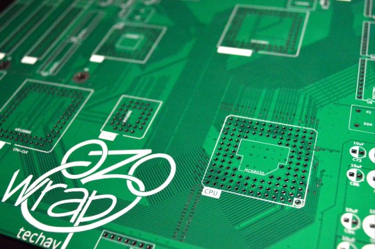
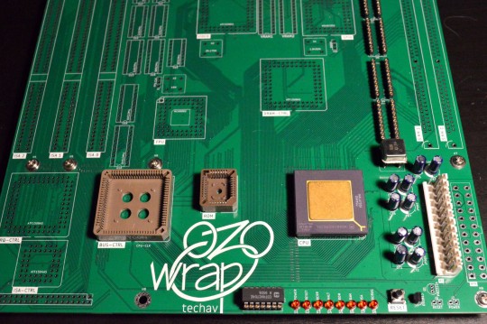
This is the largest, most complex PCB I have ever designed — a 9.6x9.6 inch (244x244mm) square, 4-layer, complete motherboard for my MC68030 homebrew computer project.
It is designed to support the Motorola MC68030 CPU, MC68882 FPU, two 72-pin SIMM sockets, 512kB ROM, two serial ports, one parallel port, PS/2 keyboard, 4-bpp VGA video, IDE hard drive, and three ISA expansion slots. A complete system all in a microATX form factor.
This builds on my previous work with the 68030, based heavily on my wire-wrap project and the boards that followed. It's a project over four years in the making. I have made a few improvements on the old design, like 16550-compatible serial ports and an updated memory map to support much more RAM in a contiguous space.
Keeping with my existing system designs, I've combined most of the logic into a set of CPLDs. This makes things like PCB layout and logic debugging so much easier. Most of the remaining discrete logic on the board is 74'245 bus transceivers for driving memory and the ISA slots.
I've kept the name "wrap030" in honor of the project's origin as a wire-wrapped prototype, despite the move to proper PCBs. It's just what I've been calling the project in my own head (and design files) all this time, so at this point no other name would feel right.

I of course wasted no time starting to assemble one, but I did stop myself from getting too carried away with the soldering iron. I want to be methodical and test each section before moving on to the next.
I have already found one major error in my board layout — the footprint for the VGA connector is backwards. I may need to bodge together some kind of adapter.
So far I've confirmed the minimalist AT power supply section works with no major shorts on power supply rails, and the reset circuit is working as expected. Next step is to try a free run test with the CPU to ensure the system clock and CPU are working. Once that is confirmed working, I can start loading logic for accessing ROM. My goal is to have it at least running BASIC on a serial terminal by VCFSW in June.
I've forked my existing wrap030 repository on GitHub for this new Wrap030-ATX, since it does make some breaking changes that will require updates to logic and programs. New repo is here:
#homebrew computing#mc68030#motorola#motorola 68k#motorola 68030#vintage computing#jlcpcb#vcf southwest#wrap030-atx
32 notes
·
View notes
Text
SE Exp30

I ordered some boards for my Mac SE accelerator. I'm quite pleased with how they look.


Assembly wasn't too bad. The 0805-size resistors and capacitors can be a bit fiddly to work by hand, but they're still manageable. In all, it just took a couple hours to put together the first test board.

It fits in my SE with plenty of clearance between it and the floppy drive cages.
So the big question is — does it work?

Of course not! What fun would that be?
First run attempt was just a garbled screen, and not even the infamous checkerboard pattern. I didn't expect it to be fully functional at first attempt, but that pattern is a new one.
Time for the logic analyzer.
I can see the hand-off working. The accelerator asserts the Bus Request signal to take the SE 68000 off the bus, and waits for the Bus Grant signal in response. Once the 68000 is off the bus, the 68030 is brought out of reset and allowed to take over. That much worked as expected.
Next thing to look at is whether the 68030 is starting up properly. The first thing it's going to do is load the initial startup vector and stack pointer from ROM. These are 32-bit values, so each will take two access cycles over the 16-bit SE bus. It was getting stuck on these initial read cycles, waiting for a bus termination signal
The 68k processor family has a great asynchronous bus that relies on peripherals providing an appropriate bus cycle termination signal. Macintosh computers generate the termination signal synchronous to the system clock. What I found was the faster 68030 (running at 12MHz for testing) was sometimes ending one cycle and starting the next within a single clock pulse of the main 8MHz SE clock. The SE motherboard logic never saw the new CPU cycle begin.
My first draft of logic was largely asynchronous, and paid little attention to the system clock. But since the SE motherboard logic is synchronous and expecting 68000 bus cycles, I need my logic to better emulate 68000 bus cycles.
So I rewrote nearly all of the logic for the CPLD to roughly emulate 68000 bus cycles.

Never thought I'd be happy to see a Sad Mac error. That error means the 68030 is running enough code for the initial ROM checksum to fail. That's quite an improvement over not even loading the initial vectors.
I've got a long way to go on this project, but it's looking promising. Running any code at all is a great sign. I can already see a the next few logic bugs that need to be addressed, and I've found a few hardware bugs that'll need bodge wires.
#debugging#mc68030#macintosh#motorola 68k#mac se#exp30#mc68882#mc68000#vintage computing#homebrew computing
30 notes
·
View notes
Note
Hi, I saw your post in regard to the 68882. I had the same problem and also got protocol errors. Careful inspection of the 68881/68882 manual page section 10.3 that the CS of the FPU should be asserted before AS/ of the processor. When I removed the as = '0' from my vhdl the FPU worked correct.
Oh wow good catch!
"A timing restriction on CS# is that it must be either negated or asserted during transitions of the AS# and DS# signals. Thus, CS# must either be asserted before AS# or DS# is asserted at the start of a bus cycle, or it must remain negated until after the strobe signals are stable ..."
I'll have to give that a shot. I'm quite certain I had qualified the CS# signal with AS# just out of habit.
4 notes
·
View notes
Text


Challenges
Getting the MC68882 Floating Point Coprocessor working has been much more challenging than I expected. The timing or noise or whatever problems that were preventing me from running the main board at full speed are only compounded by trying to add a second board. The computer would fail to properly load BASIC into RAM. I tried rewiring the data bus on the mezzanine board three times with very limited improvement.


In the end I had to slow down the machine yet again. The 25MHz CPU is only rated down to 12.5MHz but now I'm having to run it at 6MHz just so it can get through loading BASIC. And still it gives coprocessor protocol error when testing FPU instructions. Although that is an improvement because that means the FPU is communicating enough to throw the protocol error.
Now I still don't have an oscilloscope to try to see what is going wrong, so I have to resort to trial and error debugging. An important part of transmission line theory (a subject for which I have very limited understanding) involves proper termination, so I tested that. The old VMEbus specification (designed originally for 68k CPUs) specified 470/330 ohm terminating resistors, so that's where I started.


I added terminating resistors to the data and address lines on the main board right by the main header. The results were ...

well disastrous, really. I had only made it worse. I tried different value resistors and ultimately removed the terminating resistors and their wiring altogether. And it still didn't work. In fact, everything I tried seemed to make things even worse. It got to the point where no matter what speed I tried running the machine, the terminal would just output unrecognisable garbage.
Time to pull out the logic analyzer. I eventually realized that despite the garbage on the terminal, the UART was actually outputting valid data. It was just getting lost in translation. That's when I realized I had the MAX232 serial level shifter wired wrong all this time. When I was adding in the terminating resistors in the vicinity of the MAX232 I must have bumped it or something and broke whatever spell had it working previously. I fixed the error and eventually got the system running again at 6MHz.
I'm still getting protocol errors sometimes when trying to use the FPU, but there have been a few times where I was able to tell it to add 2+3 and get a proper response in return.

Ultimately though the system is already very unstable. I'm not sure I will be able to wire in another part and still be able to get it to run. I very well may have reached the limit of what this densely-packed wire-wrapped monstrosity can do. I've worked on nothing else for six months of weekends and I think it might be time to take a break and work on something else for a while.
39 notes
·
View notes
Text
Moving Up
I decided to move forward with the 68030 project at half speed since I don't have the tools to troubleshoot why it won't run any faster. Ultimately I would like to run a proper operating system on this thing, but the *nix systems I've looked at all require at least 8MB of RAM. BSD and 68k Linux also require the 68882 maths coprocessor as well. And of course, I'll need some kind of storage device.
I've been planning a mezzanine board that would sit on top of the main board with a couple ribbon cables to connect them. I don't have enough space for full 32-bit data an address busses to be broken out, so I'm planning on a 16-bit data bus. I should have just enough room for FPU, two 30-pin SIMM sockets, an IDE header, buffers and glue logic, and an 8-bit ISA slot just in case. It's a very tight fit, but would make for a complete system.

I've started with wiring the FPU because the only additional logic it requires is chip select, which I can handle entirely by a single 74'521 8-bit comparator. After the FPU is tested and working, IDE will be the next thing needed, since it should allow for easier testing from here out. IDE will actually sit on the ISA bus, so ISA will naturally come with it. There is quite a bit of logic required for timing and buffering, so I'll need to program the CPLD. DRAM will come last and will be the most challenging because of the multiplexed address bus, refresh timing, etc.


34 notes
·
View notes