#USB Zener diode
Explore tagged Tumblr posts
Visit Tumblr Blog
Explore Tumblr blogs with no restrictions, modern design and the best experience.
Last Seen Tumblr Blogs


Fun Fact
Tumblr is available in 18 languages.
Text
https://www.futureelectronics.com/p/electromechanical--circuit-protection--tvs-diodes/pesd1can-215-nexperia-6297154
USB Zener diode, Transient voltage suppression, Bidirectional TVS diode
PESD1CAN Series 70 V 17 pF SMT CAN Bus ESD Protection Diode - SOT-23
#Circuit Protection Devices#TVS Diodes#PESD1CAN#215#Nexperia#USB Zener diode#Transient voltage suppression#Bidirectional TVS diode#surge suppressor#LDO Voltage Regulator#Zener diode#application#TVS diode#transient voltage suppression diode
1 note
·
View note
Text
https://www.futureelectronics.com/p/electromechanical--circuit-protection--tvs-diodes/lc03-3-3-tbt-semtech-5141093
Transient voltage suppressor diode, TVS diode application, Bi-directional TVS
LC Series 18 V 1800 W SMT Low Capacitance TVS for High Speed Interface - SOIC-8
#Semtech#LC03-3.3.TBT#Circuit Protection Devices#TVS Diodes#transient voltage suppressor diode#TVS diode application#Bi-directional TVS#Zener diodes#electro-static discharge#suppression diode#Silicon-avalanche diodes#array#TVS USB diode
2 notes
·
View notes
Text
https://www.futureelectronics.com/p/electromechanical--circuit-protection--tvs-diodes/ptvs30vs1ur-115-nexperia-3027558
TVS diode manufacturers, TVS diode array, Diode circuit, TVS protection
PTVS Series 400 W 48.4 V Uni-Directional Surface Mount TVS Diode - SOD-123W
#Nexperia#PTVS30VS1UR#115#Circuit Protection Devices#TVS Diodes#manufacturers#TVS diode array#Diode circuit#TVS protection#transient voltage suppressor diode circuit#diode#Zener#application#Bi- Directionnel TVS diode#USB
1 note
·
View note
Text
https://www.futureelectronics.com/p/electromechanical--circuit-protection--tvs-diodes/sm6t36cay-stmicroelectronics-6152925
USB TVS diode, Bidirectional Zener diode, diode circuit, Diode arrays,
SM6T Series 600 W 36 V Bi Directional Transient Voltage Suppressor - DO-214AA
#STMicroelectronics#SM6T36CAY#Circuit Protection Devices#TVS Diodes#USB#Bidirectional Zener diode#diode circuit#Diode arrays#selection#Bi-Directional#Transient-voltage-suppression#High-voltage transients#TVS Surge Protection
1 note
·
View note
Text
https://www.futureelectronics.com/p/electromechanical--circuit-protection--tvs-diodes/usblc6-4sc6-stmicroelectronics-7131158
USB TVS diode array, Transient voltage suppressors, ultra-high-speed interfaces
USBLC6 Series 4 Line 6 V Uni / Bi-Directional ESD Protection - SOT-23-6
#STMicroelectronics#USBLC6-4SC6#Circuit Protection Devices#TVS Diodes#Array#TVS diode circuit#Transient-voltage-suppression diode#USB#Transient voltage suppressors#ultra-high-speed interfaces#TVS diode clamping voltage#TVS diode vs Zener
1 note
·
View note
Text
https://www.futureelectronics.com/p/electromechanical--circuit-protection--tvs-diodes/sm6t36cay-stmicroelectronics-6152925
Transient voltage suppressor, diode circuit, High voltage tvs diode
SM6T Series 600 W 36 V Bi Directional Transient Voltage Suppressor - DO-214AA
#STMicroelectronics#SM6T36CAY#Circuit Protection Devices#TVS Diodes#Electrostatic discharge#suppression diode#diode circuit#transient voltage suppressor#Transient voltage suppression diode#TVS Zener#Diode array#USB TVS Diodes
1 note
·
View note
Text
https://www.futureelectronics.com/p/electromechanical--circuit-protection--tvs-diodes/sm712-02htg-littelfuse-9049160
Transient voltage suppression diode, TVS diodes for USB, TVS diode application
SM712 Series 31 V 600 W Surface Mount Asymmetrical TVS Diode Array - SOT-23-3
#Littelfuse#SM712-02HTG#Circuit Protection Devices#TVS Diodes#Surface Mount Zener#Bidirectional#Transient voltage suppression diode#TVS diodes for USB#TVS diode application#Current controller#Zener diode#high voltage tvs diode
1 note
·
View note
Text
TVS diode array, TVS Zener diode, Electrical high voltage, Bidirectionnel TVS
SM6T Series 600 W 36 V Bi Directional Transient Voltage Suppressor - DO-214AA
#STMicroelectronics#SM6T36CAY#Circuit Protection Devices#TVS Diodes#High-voltage transients#array#TVS Zener diode#Bidirectional#Electrical high voltage#USB#Diode circuit#manufacturers#Transient voltage suppressor diode#selection
1 note
·
View note
Text
TVS zener diode, diodes, voltage surge suppresseur, Bidirectionnel TVS diode
SMBJ Series 600 W 32.7 V Bi Directional Transient Voltage Suppressor - DO-214AA
#Circuit Protection Devices#TVS Diodes#SMBJ28CA-TR#STMicroelectronics#TVS diodes for USB#TVS zener diode#arrays#Transient voltage suppressor#tvs diode clamping voltage#circuit#transient voltage suppression diode circuit#USB Isolator
1 note
·
View note
Text
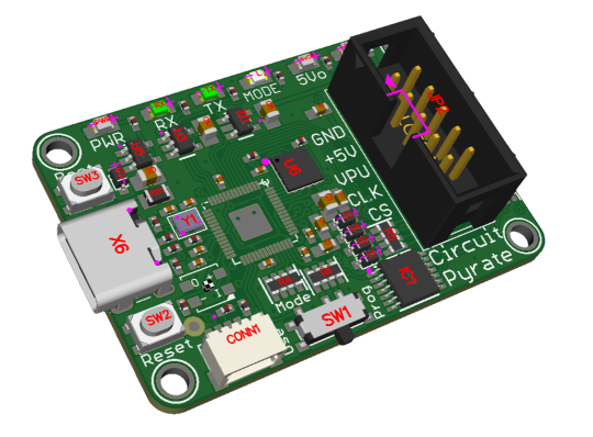

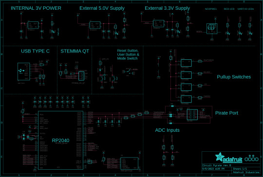

yaaarrr! a Circuit Pyrate is ready to be your best mate on the hacking seas
⚓️🏴☠️🤖🔧💻🔗🐍🔋📚💡🔌✨🌐💬📌🔄🔍💼📊
we recently sold out of our stock of Bus Pirates https://github.com/BusPirate/Bus_Pirate and when we booked a reorder we found it's currently unavailable with no ETA for re-stocking. it made us think about revisiting this design, perhaps using an RP2040 instead: with native USB and CircuitPython and PIO it might be easier to add new protocols! we did do a "Circuit Pyrate" draft many years ago but it was based on the SAMD21 and we quickly ran out of space - another thing the RP2040 would excel at.
parsing data is something that Python does very well, and tannewt already has VT100 control code support for the REPL status bar, so we're having a go at re-implementing the UX in native python by instantiating a secondary 'data only' CDC UART endpoint https://learn.adafruit.com/customizing-usb-devices-in-circuitpython/circuitpy-midi-serial#usb-serial-console-repl-and-data-3096590 The default REPL can then be enabled or disabled with the onboard slide switch.
here's our draft that uses the same sizing and header location but of course all different parts. two challenges: the RP2040 is not 5V-tolerant like the PIC24J but it's also not guaranteed for high speeds, so we put a 1K+3.6V zener diode on the 4 GPIO pins that ought to let it work OK with 3 or 5V devices. secondly, the pin mux distribution for I2C and UART doesnt match the same as the original chip so we may have to PIO bitbang those interfaces. we're going to have to do a bunch of pin twiddling to find out the limitations of this design. we add a separate Stemma QT port, NeoPixel, and LEDs for both power outputs. fun fact, did you know that the bus pirate is CC-0 http://dangerousprototypes.com/docs/Bus_Pirate_v3.6#License a rarely seen license for OSHW!
our current pondering is how to best mimic the 5V tolerant inputs of the PIC24J - the 1K + 3.6V zener will definitely do the job but can slow down the IO quite a bit on those high speed SPI lines. because we want full bidirectional support for each pin and be able to enable/disable optional 10K pullups to 3V (internal) or 5V (external) we can't us the TXS0104 series: has built in un-disableable pullups. this app note has a few tips we're perusing https://ww1.microchip.com/downloads/en/DeviceDoc/chapter%208.pdf - #11 looks like it may work..any suggestions?
8 notes
·
View notes
Text
TVS Zener diodes
My study was about TVS Zener diodes, USB Diode array and Circuit Protection Devices, TVS Diodes, PESD1CAN,215, Nexperia.
0 notes
Text
Voltage suppression, diodes, tvs diode application, tvs diode capacitance
SMCJ Series 30 V 1500 W SMT BI-directional Transient Voltage Suppressor
#Circuit Protection Devices#TVS Diodes#SMCJ30CA-13-F#Diodes Incorporated#diodes#tvs diode application#tvs diode capacitance#Bidirectional TVS diode#TVS zener diode#usb tvs diode array#Transient voltage surge suppressor#tvs diode array
1 note
·
View note
Text
High-voltage transients, tvs diode array, TVS zener diode, Bidirectional TVS
USBLC6 Series 4 Line 6 V Uni / Bi-Directional ESD Protection - SOT-23-6
#Circuit Protection Devices#TVS Diodes#USBLC6-4SC6#STMicroelectronics#high-voltage transients#tvs diode array#TVS zener diode#Bidirectional TVS#usb tvs diode array#Diode circuit#Transient voltage suppressor diode#selection
1 note
·
View note
Text
https://www.futureelectronics.com/p/electromechanical--circuit-protection--tvs-diodes/pesd1can-215-nexperia-9227406
What Is a transient voltage suppression, usb protection circuit
PESD1CAN Series 70 V 17 pF SMT CAN Bus ESD Protection Diode - SOT-23
#Nexperia#PESD1CAN#215#Circuit Protection Devices#TVS Diodes#What Is a transient voltage suppression#usb protection circuit#usb tvs diode array#Transient Voltage Suppressor Diode#High voltage tvs diode#TVS Zener diode#diode circuit#usb short circuit protection#Diode array
1 note
·
View note
Text
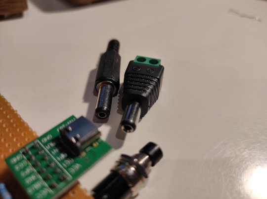
Business in the front, party in the back. Yes, I'm leaving the button like that. It's fine.
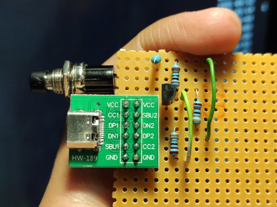

This is a Qualcomm Quickcharge Trigger, based loosely on this design, but only rigged for 12V.
When you press the button, it negotiates up from 5V to 12V from any QC 2.0 compatible charger.
Why? The 12V supply that runs my desk is a noisy, cheap pile of garbage that whines at 18kHz all the time, and my hearing is still good enough to hear that all goddamn night. Finding quiet 12V supplies that don't develop inscrutable hums a few months down the line is a crapshoot. On the other hand, cellphone chargers are usually impossibly quiet. I have a loose QC phone charger that I don't need for anything else, so if I can convince it to pump out 12V I can use that to run my desk. Hence, this pile of junk.
Tested and working, all I have to do is press the button to get it to put out 12V. Eventually I might get a 9V zener diode and an LED and set up an indicator that tells me if it's in 12V mode, but for now I'll lean on the fact that I built it and I know how it works.
This is NOT fully wired correctly, as in if you plug the USB cable in upside down it will not trigger correctly. Fixing this is not too hard but would require me to fuck around with the protoboard more than I already have and dealing with protoboard is miserable. I'll just put some alignment markers on the cable I'm using I guess.
I'll have to sit later with a hacksaw and cut this section of protoboard out. Bleh. Building a case for things like this is what makes me wish I had a 3D printer. The exposed pins on the bottom are a short risk so this will get a chunk of cardboard two-way taped to the bottom.
If you ever get a chance to stock up on industry standard barrel jacks, do it, I use these things everywhere.
Quickcharge is a dying protocol, being replaced almost wholly by USB-PD, but USB-PD requires putting an actual microcontroller in the mix whereas this can be done fully analogue, and I believe that even QC 3.0 is still simple enough that a human with some buttons and a few resistor ladders could query basically any voltage it can supply (which is many)
71 notes
·
View notes
Text
TP4056 1A Li-ion lithium Battery Charging Module Charging Board Charger TP 4056 - Mini USB
New Post has been published on https://apzweb.com/tp4056-1a-li-ion-lithium-battery-charging-module-charging-board-charger-tp-4056-mini-usb/
TP4056 1A Li-ion lithium Battery Charging Module Charging Board Charger TP 4056 - Mini USB


Price: (as of Jan 01,1970 00:00:00 UTC – Details)

TP4056 1A Li-ion lithium Battery Charging Module Charging Board Charger TP 4056 In the product image there are 2 similar items joint together, there will be only one item sold in this listing. Power: Medium Power Brand Name: TP4056 Usage: Zener Diode Structure: PNP Special Function: Common Point Contact Diode Frequency: High Frequency Type: Power Module Construction: Planar Type Material: Silicon Install Style: SMD Function: Power Triode Model Number: TP4056.
Onboard MINI USB head can directly link computer USB port charging The charging board can also be powered by pin (IN + and IN-) Reserved the TEMP pin header, and can be used as a lithium battery temperature detection PCB board size: 3.73 (cm) x1.5 (cm)/1.46”X0.59” Input voltage: 4V-8V maximum output charging current: 1000mA
0 notes