#PCB design guidelines
Explore tagged Tumblr posts
Visit Tumblr Blog
Explore Tumblr blogs with no restrictions, modern design and the best experience.
Last Seen Tumblr Blogs


Fun Fact
130K people were victims of a chain letter scam that affected Tumblr in May 2011.
Text
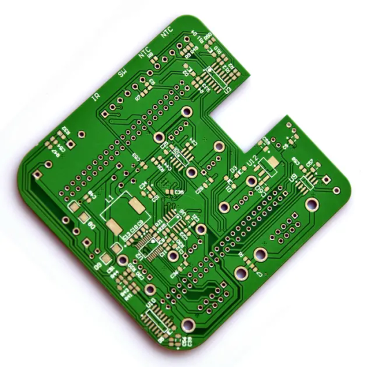
Tips to design High Frequency PCB for optimal performance
Best practices for high-frequency PCB design with PCB Power. Our guide provides comprehensive PCB design guidelines, material selection tips, and advanced techniques for superior performance. As a leader in PCB manufacturing in the USA, PCB Power ensures top-quality production and expert advice. Learn how to optimize impedance, grounding, and signal integrity. Visit PCB Power's Video for more details!
0 notes
Text
0 notes
Text
4 Crucial Things to Consider While Choosing LED PCB Manufacturer
LEDs have revolutionized lighting. At the heart of their brilliance, is the PCB assembly. Electing the right LED PCB assembly manufacturer can make or break your project. This ensures quality, performance, and ultimately, success. So, before you dive into the luminous world of LED PCBs, this article sheds some light on the key factors to consider when making your purchase:
1. Experience Matters: You should choose a manufacturer with proven expertise in LED PCB assembly. The company you choose should have a track record of successful projects similar to yours. Experience means they will understand your specific needs and deliver assemblies that meet or exceed your expectations.
2. Material Matters: The heart of your PCB is its materials. Go for manufacturers
who ensure high-quality FR4 or metal-core PCBs for optimal thermal management and longevity. They must adhere to industry standards for materials and components to guarantee reliability and safety.
3. Thermal Management: LEDs are designed to generate heat, so proper thermal management plays a crucial role. Look for manufacturers who offer solutions like aluminium heat sinks. Their expertise in thermal management can extend the lifespan of your LED PCB and prevent overheating issues.
4. Price is Not Everything: Though cost is important, its priority is not over quality.
The cheapest option might have hidden costs in the long run. Choose a manufacturer who offers budget-friendly pricing while maintaining high-quality standards and reliable service.
If you are looking for an LED PCB manufacturer near you you can count on Hitech Circuits Co., Limited. They have more than 20 years of experience in the electronics manufacturing industry. They have a talented design team who follow advanced manufacturing techniques.
These guidelines help you illuminate your path to finding the perfect LED PCB assembly manufacturer. Your choice has a direct impact on the performance, lifespan, and success of your project.
2 notes
·
View notes
Text

High Volume PCB Assembly
Your leading PCB High Volume PCB Assembly supplier in China
With 15 years of experience and high efficiency in PCB assembly and manufacturing, HITECH CIRCUITS is the perfect source for Big Batch PCB assembly on a limited budget. If you are looking for a large PCBA assembly within your budget, we will be your ideal choice. HITECH CIRCUITS has more than 15 years of experience in the OEM/PCBA manufacturing and assembly of printed circuit boards, advanced production technology and equipment, professional engineers and purchasing team to provide our partners with personalized and complete process solutions. HITECH CIRCUITS’s supply chain services deliver supply chain innovation on demand. We offer a bold, yet proven service solution designed to grow market share and profit. Our innovative approach to managing the supply chain offers a complete business model that delivers the talent and transformative tools necessary to create predictability, reliability, and responsiveness across your entire supply chain. Our practitioners are passionate about supply chains. We have spent a generation understanding, refining and building the best in intelligent supply chains. We provide talent on-demand with expertise in data analytics and strategic technologies that can help you predict, plan and respond more effectively.
Some designs require assemblies in small volume, maybe just prototypes, while others require them in high volume. At SMT house, High Volume, Large Volume, or Big Batch PCB Assembly always refers to printed board assembly projects with quantities more than 5K pieces. HitechPCB has the capability to offer high volume PCB assembly services to meet your requirements of high-quality, competitive price, on-time delivery and smooth communication in any manner of full turnkey, consigned and partial turnkey.
Also, if your business is involved in applications that require high-volume PCB assembly, the company to contact is HitechPCB, because we’re a complete turnkey solution for printed circuit boards assembly, we are ideally suited for bulk PCB assembly orders. Our state-of-the-art equipments, large facility and wide range of highly-qualified experts give us the capability of high-volume PCB assembly of up to 9,000,000.
We are also the perfect source if you’re looking for large-order PCB assembly on a budget. Because of our high level of efficiency and more than 10 years of experience with printed circuit board manufacturing and electronics assembly, we offer large printed circuit board orders at surprisingly competitive prices compared to other PCB manufacturers or PCB assembly companies.
Our large order PCB assembly process starts with a tested and practiced set of workflow guidelines for every phase of the process, from pre-order PCB design consultation with professional veteran engineers to PCB fabrication, components sourcing, PCB assembly, PCBA testing, PCBA inspection, PCBA packing and shipping all under the auspices of a highly-skilled production staff. You can be confident that no matter how many circuit boards you order, you will enjoy fast service, low prices and extremely high quality.
With our excellent after-sales service, 24 sales and technical support team, quick response service, we will be your best Big Batch PCB assembly manufacturer inChina. A wide variety of highly qualified experts
Why choose Hitechpcba Big Batch PCB Assembly
Compared to our competitors, Hitechpcba offers large printed circuit board orders at very competitive prices. The risky big batch PCB assembly process begins with a set of tried and tested workflow guidelines. From ordering PCB design to component procurement, manufacturing, testing, assembly, inspection, shipping and packaging. This is all under the guidance of our highly skilled production staff.
No matter how many boards you order, you'll love the fast response service, low cost, and surprisingly high quality.
Whether you are seeking for product designer, electrical engineer, system integrator, manufacturer, or big batch PCB manufacturing and assembly, low cost big batch PCB housing, electronic assembly services, Hitech Circuits PCB Assembly team will be your perfect choice for big batch PCB assembly plant inChina.
Finding Reliable High Volume PCB Assembly Supplier?
When your design passed the prototyping verification after optimization, DFM and DFT check, it’s time to find a manufacturer or a supplier who has ability to perform high volume PCB manufacturing and assembly for you. HITECH CIRCUITS is a one-stop PCB solution provider, no matter which your design stage is located, we always can help in PCB manufacturing, assembly and design. With both design and manufacturing knowledge, we can feedback some suggestions to modify or change your design on the basis of cost-down without sacrificing the quality and performance. What’s more, if choosing our full turnkey PCB assembly service, we will be responsible of BOM sourcing to reduce your workload. Our approach to conducting high volume printed circuit board assembly is founded on a commitment to the highest possible quality, based on IPC standards and our inner quality control processes. In spirit of those high assembly standards, HITECH CIRCUITS developed excellent high-volume assembly capabilities and manufacturing processes relied on our advanced assembly lines in dust-free workshop.
Big Batch PCB Assembly: The Ultimate FAQ Guide
This guide covers all the important aspects of big batch PCB assembly.
Therefore, read this guide before starting your next PCB assembly project.
What is big batch PCB assembly?
Do you have lead-free mass PCB assembly?
What is the testing protocol for mass PCB assembly?
Do you have a custom mass PCB assembly?
How does small batch PCB assembly compare to large batch PCB assembly?
What are the main capabilities of mass PCB assembly?
What are the applications of mass PCB assembly?
What is the cost of mass PCB assembly?
How safe is the mass PCB assembly process?
Do you provide both THT and SMT in big batch PCB assembly?
What is the turnaround time for mass PCB assembly?
What are the quality certifications for mass PCB assembly?
What to consider when choosing big batch PCB assembly services?
Why is it difficult to scale up from prototype to high-volume assembly?
How do you simplify the transition from prototype to mass PCB assembly?
What is big batch PCB assembly?
Big batch PCB assembly is an assembly process where you will assemble 10,000 or more PCBs in a specific period of time. The main processes you will use to assemble PCBs in large quantities are design for manufacturing and design for testing.
What are the advantages of using big batch PCB assembly? PCB assembly process
With applications in mind, big batch PCB assembly will provide you with numerous industrial and personal benefits. This is why electronic OEM prefer to use it in most of their applications.
The following are the main advantages of using mass printed circuit components:
Rapid design and prototyping process
Since you will be mass-producing or manufacturing printed circuit boards, you must assemble them uniformly. By simply creating a design and a prototype that works for each PCB, you can save a lot of time.
Short production cycle
Since the production process is fully automatic, you will also save time in the production of numerous PCBS. It all starts with the design and prototyping phase, which you'll do with the help of software and machines.
Production consistency
You will also have a very uniform production process because most of the details are predetermined before implementation. Once production begins, all manufacturing specifications will follow uniform specifications for all printed circuit boards.
Quality consistency
Since you will be producing all PCBs to similar specifications, you will automatically get consistent quality throughout the production process. In other words, you should rest easy knowing that you will have consistency across all printed boards.
First-class cost performance
This is the most convenient model for the cost of producing printed circuit boards because you can do everything very consistently. Here, you will buy all the materials in bulk and produce them in a short time using similar machines.
Improve the market's ability to time
You will be able to produce large number of printed circuit boards in a very short time, thus giving you the advantage in the market. In other words, you will have a steady supply of on-demand printed circuit boards, giving you the advantage in the market.
Do you have lead-free mass PCB assembly?
Yes, we care about the health of our users and the health of the environment. We are aware of the harmful or negative effects that lead emissions can have on users and the environment.That's why we eliminate lead from production materials. It is of great benefit to protect people's health and eliminate environmental pollution.
What is the testing protocol for mass PCB assembly?
As long as you have completed the process of producing printed circuit boards, you must ensure that they run well.
Existing testing protocols will help ensure that large volumes of PCBs are in perfect working condition.
Here are the main test protocols you can perform on a high volume printed circuit board:
Automated Optical Inspection (AOI)
You will use Automated Optical Inspection (AOI) tools to accurately and efficiently detect production errors in big batch PCB assembly. It has cameras and image-processing software that can identify assembly errors and relay information for further action. It is the best tool you will use for better error detection than visual inspection.
Solder Paste Inspection (SPI)
After you have finished printing with the paste printer, you must pass it through the paste inspector. The SPI machine has a camera and communication system equipment that can examine every detail of the solder paste.It compares these details to the Gerber file and reports any kind of inconsistency.
In-Circuit Test (ICT)
In-Circuit Test, you can use the most detailed test methods to check the quality and integrity of the PCB.Here, you will have to take personal initiative and use online testing software to check the quality of your PCB.You will use the machine to detect errors in the PCB for correction.
Functional Circuit Test
Here, you will use a computer with test pins or test probes to test the functional integrity of the PCB. You can tell if the board passes the test simply by comparing the results to the design specifications.
X-ray Examination
You will use X-ray inspection to detect welding problems on the PCB that are not visible to the human eye. Here, you do not have to cut through the circuit board to see the welding quality on the printed circuit board. You'll use X-ray inspection protocols to detect errors in components and soldering on circuit boards.
Do you have a custom mass PCB assembly?
Yes, we do customize mass printed circuit boards.
You can order the most unique types of printed circuit boards and we will produce them according to your needs.
We'll review your design, create a prototype, and then test how it works.
Once we confirm that it is working well according to the design details, we will proceed with the production process.
How does small batch PCB assembly compare to large batch PCB assembly?
On the production scale, you can choose between large batch PCB assembly or small batch PCB assembly.
Mass PCB assembly is the process by which you assemble 10,000 or more printed circuit boards.
It is a mass production or assembly system that can mass produce PCBs in a short period of time.
On the other hand, you can choose to assemble PCBs in small batches for small scale production or assembly of PCBs.
In other words, you will produce a very small number of printed circuit boards of 250 or less.
In large and small batch PCB assembly, the assembly process will remain the same.
In addition, you will use similar detection techniques for high - and small-lot PCB assemblies.
What are the main capabilities of mass PCB assembly?
Well, when you're looking for a good large volume PCB assembler, there are some special features.
This means that they must have the specific resources that you will use in the PCB assembly process.
The following are the main functions that must be available for mass PCB assembly.
Manufacturing capacity
It is important to have a manufacturer that can use both surface mount technology and through-hole technology.
You must find a manufacturer with sufficient knowledge and experience in surface mount technology and through-hole technology.
Fast turnaround time
You should also have a manufacturer that can produce large number of PCBs in a very short time.
In other words, you don't have to wait longer to get the printed circuit board you ordered.
Welding capacity
In this case, the key point you must pay close attention to is the ability to weld manually and by machine.Your manufacturer should be able to perform both hand and machine welds.
Quality compliance
You should also know that the quality of the printed circuit board is a top priority when it comes to durability and safety.
Here, your manufacturer must have the knowledge to read the list of materials and identify the right quality products.
Test method
You must also choose a manufacturer that has knowledge of all test machines and printed circuit boards.
In other words, after production, your supplier must test all printed boards accordingly before providing PCBs.
What are the applications of mass PCB assembly?
You will be mass-producing large volume PCB assemblies of different equipment at high rates.
If you want to enter the PCB production market, you must have knowledge of mass PCB assembly.
Here are some industries that require big batch PCB assembly.
The communications industry mass-produces communications equipment
Military or defense industry
Automobile industry
Aviation industry
You will be using big batch PCB assembly in an industry where big batch production, consistency, and consistency are important.
What is the cost of mass PCB assembly?
Well, the cost of mass-producing printed circuit boards is fairly affordable.
Here, you will apply economies of scale in the production process, thereby reducing the cost of producing PCBs.
In addition, other factors that affect cost such as quality and size will also play an important role.
You will spend more on high quality and larger PCB materials, increasing production costs.
Typically, the amount you will spend usually depends on the design specifications of your PCB.
How safe is the mass PCB assembly process?
Well, most of the manufacturing process for big batch PCBs is highly automated.
In other words, there was little human involvement other than the design and programming of the machine.
In addition, we eliminate any material that would suspend harm to the environment and users.
This makes mass PCB assembly one of the safest modes for producing printed circuit boards.
Do you provide both THT and SMT in big batch PCB assembly?
Yes, we have both through-hole technology and surface mount technology for PCB assembly.
These are the main manufacturing methods we use to produce high quality printed circuit boards.
You will choose among these manufacturing modes based on the design and application specifications.
Is there turnkey assembly for large volume PCB assembly?
Of course, our production system is capable of handling very large volumes of turnkey PCBs.
You'll find products that you can buy in bulk to meet your production needs.
Here, we will be responsible for every step of production from design, inspection, prototyping and assembly.
What is the turnaround time for mass PCB assembly?
You should rest easy knowing that your production specifications will be met as planned.
This includes time for all production specifications and you will accordingly meet all your market needs.
What are the quality certifications for mass PCB assembly?
As we mass-produce printed circuit boards, we also ensure consistent quality.
This means that you will get the highest quality printed circuit boards in large quantities at an affordable price.
Our quality meets and exceeds international quality standards, namely:
Comply with IPC quality standards such as IPC-WHMA-A-610 and IPC-CC-830B
ANSI/AHRI quality standards, such as ANSI/J-STD-001 -- Class II and III only
RoHS quality certification
UL quality standard
CE quality standard
What to consider when choosing big batch PCB assembly services?
You'll see the manufacturing capabilities of high-volume PCB assemblers.
Here are the main factors that you must pay close attention to:
Manufacturing and service capabilities
QC
Years of manufacturer experience
Customization capability
Turnaround time
Responsiveness and flexibility
Delivery service
Why is it difficult to scale up from prototype to high-volume assembly?
Scaling up from low-volume to high-volume PCB assembly can prove to be a difficult and painful process.
Here are the main reasons why this can pose a difficult challenge.
You must change design files and formats to meet new design requirements
You may also lack the correct type of machine for the new specification
You may also have to change components that will be tied to the PCB
You may also have to change the entire design to accommodate the new specifications
How do you simplify the transition from prototyping to high-volume PCB assembly?
Despite the difficulties, you should rest easy knowing that you can easily complete the process.
The best way is to choose the best prototype CM that can collaborate all the details accordingly.
It will help remove obstacles that can cause confusion and make the process difficult.
At Hitech Circuits, we will help you with the PCB fabrication and PCB assembly process.
Contact us today for all of your big batch PCB assembly needs.
Parts Quality Guarantee and Reliable Testing Methods
For verifying your turnkey orders, HITECH CIRCUITS would like to provide Prior PCB assembly service, which we will assemble 3-5pcs of your PCBs ahead of the main assembly production run, and ship these prior PCBAs to you for testing. This service is totally free of charge and only available for full turnkey PCB assembly orders in high volumes, which means HITECH CIRCUITS handling PCB fabrication, Components sourcing, and final assembly for your project. In this way, you can work with our assembly team to ensure that the finished product exactly meets your specifications every time. No one knows your design as well as you do, and so we offer prior Electronics Manufacturing assembly service as a guarantee that each and every board leaving our PCB and SMT facilities will meet your own personal standards in quality and performance. Of course, this is flexible threshold; we also would like to provide prior PCB assembly service for some smaller orders if they incorporate a high degree of complexity. Prior PCB assembly is especially popular among our customers who require IC programming services, since it allows for them to ensure that their source code will function as expected on the finished assembled boards, before their full order is assembled.
0 notes
Text
Price: [price_with_discount] (as of [price_update_date] - Details) [ad_1] Hitachi's Expandable AC expands its capacity in adverse temperature conditions, it cuts down humidity inside the room and achieves set temperature faster. Split AC with Inverter compressor: Variable speed compressor which adjusts power depending on heat load. With the Sleep mode feature in this air conditioner, you can experience optimal cooling designed to keep your nights comfortable. If you encounter any issues with this AC, its error code system can guide you to a speedy resolution. Energy Rating : 3 Star - Best in class efficiency | Annual Energy Consumption: 813.13 Units Per Year| ISEER Value: 5.02 The star rating is as per BEE guidelines Copper Condenser Coil: Better cooling and requires low maintenance / Eco Friendly gas / Manufacturer Warranty: 1 Year Comprehensive on Product |10 years on Compressor| 5 years on PCB/ Controller. Auto Mode, Cool Mode, Fan Mode, Dry Mode (better humidity control), LCD Remote Control, Auto Fan Speed, Auto Restart, Green Refrigerant, 43 Quality Test features are available.Super Silent fan speed & at a distance of 1 m. [ad_2]
0 notes
Text
Using Cutting-Edge Standards and Techniques to Maximize Performance in PCB Design

Have you ever wondered what drives the functionality of your electronics? With PCB design, gadgets like computers and smartphones have ingrained themselves into our daily lives. However, did you know that every electronic gadget has a little-known hero at its core who makes everything possible? It is known as a printed circuit board, or PCB, and it is the unsung hero deserving of much greater recognition. Actually, with state-of-the-art methods and standards that can elevate your gadgets, PCB design has evolved into a kind of art unto itself. Prepare accordingly! We'll delve deeply into the field of PCB design in this post, examining the most recent methods and guidelines that can help you get the most out of your electronics and improve their performance. So grab a seat, and get ready to explore the fascinating field of PCB design! Printed circuit board (PCB) design is now more complex than just connecting the dots. PCB designers must use cutting-edge methods and follow the most recent standards because technology is developing at a breakneck pace in order to maximize performance. The field of PCB design offers a plethora of fascinating opportunities, ranging from sophisticated software tools to thermal management strategies.
Designers use sophisticated software tools, like 3D modeling software and simulation tools, to produce effective and dependable PCBs. With the aid of these tools, designers can minimize signal interference, lower noise, and optimize component placement and routing. Mixed-signal and high-speed digital printed circuit boards are also essential for optimizing performance. High-speed data transfer and complex signal processing are features that these PCBs are made to handle, and their designers had to consider things like power distribution, signal integrity, and electromagnetic interference.
Techniques for managing heat are another crucial component of PCB design. Electronic equipment produces heat, which can hinder operation and possibly result in failure if it is not properly dissipated. Thermal vias, heat sinks, and thermal pads are tools used by designers to disperse heat into the surrounding area and away from vital components. The performance of PCBs is also significantly influenced by the manufacturing process. The newest manufacturing techniques frequently make use of advanced materials like copper-clad laminates and surface mount technology. By directly attaching components to the PCB's surface, surface mount technology helps to minimize the device's size and weight.
Wrapping up
Using the most recent methods and standards while optimizing performance is the essence of PCB design art. Designers are able to produce PCBs that are dependable, efficient, and fit the requirements of contemporary electronic devices by utilizing sophisticated software tools, high-speed digital and mixed-signal PCBs, thermal management strategies, and sophisticated manufacturing processes.
At Silicon Signals, we recognize the value of state-of-the-art PCB design methodologies and guidelines. Our ability to design and develop high-speed digital and mixed-signal PCBs allows us to assist clients in achieving the performance levels they have set for themselves. Whether you require help with advanced manufacturing processes, thermal management, or PCB design, we are dedicated to providing creative and reliable engineering solutions that satisfy the demands of contemporary electronic devices. Silicon Signals is the only company you need to consider if you need assistance with PCB design. To find out more about how we can assist you in upgrading your electronic devices, get in touch with us right now.
#embeddedsoftware#embeddedsystems#embeddedtechnology#linux kernel#android#linuxdebugging#androidbsp#aosp#iotsolutions#iot development services#pcb manufacturer
0 notes
Text
What are creepage and clearance distances in electronics [RESOLVED]

In electronics, creepage and clearance distances are critical safety parameters used to prevent electrical arcing and ensure the proper isolation between conductive components. These terms are especially important in high-voltage circuits and devices like power supplies, transformers, and insulation systems. Let’s break down both concepts: 1. Creepage Distance: Creepage distance refers to the shortest path along the surface of an insulating material between two conductive parts. Essentially, it's the distance electricity would have to travel along the surface of a material if it were to arc between two points. Creepage is influenced by factors such as: - Material type: Some materials are more prone to leakage or breakdown under high voltage. - Surface contamination: Dust, moisture, or pollution can reduce the effective creepage distance by creating conductive paths. Example: On a printed circuit board (PCB), creepage distance is the distance along the surface of the board between two conductive tracks or pins. 2. Clearance Distance: Clearance distance is the shortest straight-line distance through the air between two conductive parts. This is important because air can act as an insulator, but under high voltage, electrical arcs can form if the clearance distance is insufficient. Factors that affect clearance include: - Altitude: Higher altitudes reduce air pressure, which lowers air’s insulating ability, requiring greater clearance. - Voltage level: Higher operating voltages require larger clearance distances to prevent arcing. Example: In a transformer, clearance distance would be the shortest air gap between the high-voltage and low-voltage windings. Why These Distances Matter Both creepage and clearance are crucial for: - Safety: Preventing electric shock and fires caused by arcing or insulation breakdown. - Product reliability: Ensuring that the device operates safely over time, even in harsh environments. Standards and Guidelines Various safety standards, such as IEC 60664, UL, and EN 60950-1, define minimum required creepage and clearance distances based on factors like: - Operating voltage - Pollution degree (environmental conditions) - Insulation type (basic, supplementary, or reinforced) These distances vary depending on the application and voltage levels involved. Summary: - Creepage distance: Along the surface of the insulator, affected by surface conditions. - Clearance distance: Through the air, affected by environmental and electrical conditions. Designers must adhere to these distances to ensure compliance with safety regulations and prevent failures in electronic devices. Read the full article
0 notes
Text
The Extreme Direct to Circuit Card Assembly and PCB Board Assembly
Circuit Card Assembly (CCA) and PCB Board Assembly (PCBA) are vital components in the world of hardware. Whether you are fabricating buyer gadgets, car parts, or aviation gadgets, the Assembly of these boards plays a basic part in guaranteeing that items work accurately. In this article, we shall determine the forms, advantages, and importance of Circuit Card Assembly as well as PCB Board Assembly.
What is Circuit Card Assembly (CCA)?
Circuit Card Assembly alludes to the prepare of interfacing electronic components to a PCBA Circuit Board. This handle can be either computerized or physically performed. The reason of CCA is to make a working circuit by fastening components like resistors, capacitors, and transistors onto the PCB.
Steps Included in Circuit Card Assembly
1. Design and Format: The plan stage includes making a schematic of the circuit and laying out the PCB. Engineers plan the circuitry to guarantee legitimate functionality.
2. Component Arrangement: In the Assembly handle, components are put accurately on the board. CCA step can be performed using Surface Mount Technology (SMT) or Through-Hole Technology (THT).
3. Soldering: The components are soldered to the board once they are mounted. Patching can be performed utilizing wave patching, reflow patching, or hand fastening techniques.
4. Inspection and Testing: After Assembly, the board experiences thorough review and testing to guarantee it capacities accurately. AOI as well as X-ray inspection are widely used to detect any failure.
PCB Board Assembly (PCBA)
PCB Board Assembly (PCBA) is the handle of collecting a printed circuit board (PCB) with all the essential electronic components to make a utilitarian circuit board. It is comparative to Circuit Card Assembly but centres on the total Assembly of all components on the PCB.

Types of PCB Assembly
1. Single-Sided PCB Assembly: In this sort, components are collected as it were on one side of the board. It is commonly utilized in basic electronic devices.
2. Double-Sided PCB Assembly: The two sides of the PCB are used in setting up the components. With this, much more complex circuitry is possible, and it is one of the wide applications for advanced electronic devices.
3. Multi-Layer PCB Assembly: Multi-layer PCB Assembly implies using more than one layer of PCBs held together. This sort is perfect for progressed gadgets requiring higher complexity and more compact designs.
Key Benefits of Circuit Card and PCB Assembly
• High Unwavering quality: Well-assembled PCBs give tall unwavering quality, guaranteeing the gadget capacities without blunders over an amplified period.
• Cost-Effective Generation: The robotized Assembly of PCBs decreases labor costs, making it more cost-effective for large-scale production.
• Compact Plans: With the advancement of multi-layer PCBs, electronic gadgets can be outlined more compactly whereas keeping up functionality.
• Enhanced Execution: Appropriate Assembly and component situation make strides the in general execution of the gadget, guaranteeing productive control administration and flag transmission.
Applications of PCBA and CCA
• Consumer Electronics: Gadgets like smart phones, portable workstations, and tablets depend on exact PCB Assembly to work effectively.
• Automotive: Circuit boards are fundamental in car hardware for frameworks like route, infotainment, and security features.
• Medical Gadgets: Life-saving therapeutic gear, counting observing frameworks and symptomatic machines, depends on precise PCB assembly.
• Aerospace: Circuit boards utilized in aviation applications must meet exacting quality guidelines to guarantee tall unwavering quality beneath extraordinary conditions.
ConclusionCircuit Card Assembly and PCB Board Assembly are at the heart of advanced gadgets. They give a establishment for building utilitarian and proficient gadgets over different businesses. Whether you're in buyer gadgets, car, or aviation, understanding the significance of legitimate PCB Assembly will offer assistance you create dependable and high-performing items.
0 notes
Text
Understanding Annular Rings in PCB Design | Lion Circuits
In the world of printed circuit board (PCB) design, every detail counts, and one such detail that plays a critical role is the concept of annular rings. These features are essential for ensuring reliable electrical connections and maintaining the integrity of the PCB during the manufacturing process. At Lion Circuits, we recognize the importance of understanding annular rings and their implications for effective PCB design.
What Are Annular Rings?
Annular rings refer to the circular band of copper that surrounds a plated-through hole on a PCB. Essentially, when a hole is drilled into the board and subsequently plated, the copper forms a ring around the hole. This ring is critical because it provides a conductive pathway between the pad and the plated hole, ensuring that electrical signals can pass through without interruption.
Importance of Annular Rings
Electrical Connectivity: The primary purpose of annular rings is to establish a reliable connection between the PCB’s pads and the through-hole components. If the annular ring is too small or improperly formed, it can lead to weak or intermittent connections, which can cause circuit failures.
Mechanical Strength: Annular rings contribute to the mechanical stability of the PCB. A well-formed ring ensures that components are securely anchored to the board, reducing the risk of damage due to thermal expansion or mechanical stress.
Manufacturing Tolerance: During the PCB fabrication process, various factors can affect the integrity of annular rings, such as drilling tolerances and plating processes. Understanding how to design effective annular rings can help mitigate issues during manufacturing, leading to higher yield rates.
Designing Effective Annular Rings
When designing PCBs, it’s crucial to consider the size and dimensions of the annular rings. Here are some guidelines to follow:
Minimum Ring Width: Aim for a minimum width of 0.2 mm for the annular ring to ensure a strong connection. However, this may vary based on specific manufacturing capabilities.
Drill Hole Size: The size of the drill hole impacts the annular ring width. When designing, make sure to account for the drill size and how it will affect the resulting annular ring.
Layer Count: In multilayer PCBs, consider how the annular rings will interface between layers. Proper alignment is crucial for maintaining electrical integrity across layers.
Conclusion
Understanding annular rings is fundamental for anyone involved in PCB design and manufacturing. These features play a vital role in ensuring electrical connectivity, mechanical strength, and overall reliability of the PCB. At Lion Circuits, we emphasize the importance of precise design practices, helping you create high-quality PCBs that meet your specifications. By paying close attention to details like annular rings, you can enhance the performance and longevity of your electronic devices. If you're looking for expert guidance on PCB design or manufacturing, reach out to us today!
0 notes
Text
Tips to design High Frequency PCB for optimal performance
Explore optimized techniques for high-frequency PCB design. Learn how to minimize signal loss, reduce interference, and achieve peak performance in your advanced electronic projects with expert tips and strategies.
0 notes
Text
The Complete Guide to Studying MBBS in Russia: Admission, Fees, and Lifestyle

Introduction
Studying MBBS abroad has become an attractive option for Indian students who want quality education at affordable rates. Russia is one of the top choices due to its well-structured medical programs, affordable tuition fees, and globally recognized degrees. With over 30 medical universities in Russia approved by the Medical Council of India (MCI), students can secure a degree comparable to those offered by renowned institutions worldwide.
In this comprehensive guide, we will delve into everything you need to know about studying MBBS in Russia, covering admission requirements, tuition fees, lifestyle, and how MBBS abroad consultants like us can make the process smoother for you.
1. Why Study MBBS in Russia?
Russia has been a popular destination for students who want to pursue MBBS abroad for decades. Here are some key reasons why you should consider studying MBBS in Russia:
Globally Recognized Degrees: Russian medical universities are recognized by the World Health Organization (WHO), MCI, and other international medical councils, which means you can practice medicine worldwide after graduation.
Affordable Education: The cost of studying MBBS in Russia is significantly lower than in private medical colleges in India or Western countries. Tuition fees range from USD 3,500 to USD 7,000 per year, depending on the university.
Quality Education and Facilities: Russian medical universities are known for their modern infrastructure, well-equipped laboratories, and highly qualified faculty. The course material is designed to give students both theoretical understanding and real-world experience.
Cultural Exposure and Diversity: Studying in Russia offers students the chance to experience a rich cultural history and interact with peers from all over the world, fostering a global perspective.
Simple Admission Process: The admission process for MBBS abroad in Russia is straightforward and doesn’t require entrance exams like NEET (except for Indian students, where NEET qualification is mandatory).
2. Eligibility Criteria for MBBS in Russia
To secure admission to study MBBS in Russia, students need to meet the following eligibility criteria:
Academic Qualifications: Students must have completed their 12th grade with at least 50% marks in Physics, Chemistry, and Biology (PCB). The minimum percentage requirement may vary depending on the university.
Age Requirement: Students must be at least 17 years old by December 31 of the year of admission.
NEET Qualification: As per the latest guidelines from the Medical Council of India, Indian students must qualify for the NEET (National Eligibility cum Entrance Test) to pursue MBBS abroad.
Language Proficiency: While most universities offer MBBS programs in English, students may be required to have a basic understanding of Russian for daily communication. Many universities also offer preparatory courses for the Russian language.
3. Admission Process for MBBS in Russia
The admission process to study MBBS in Russia is simple but must be done carefully to avoid delays or rejections. Here’s a step-by-step guide:
Select a University: Research and select a suitable medical university in Russia based on factors like tuition fees, campus facilities, and MCI recognition.
Submit Application: Fill out the application form on the university’s official website. Ensure all required documents like passport, academic transcripts, and NEET score are uploaded.
Receive Admission Letter: After reviewing your application, the university will issue an admission letter confirming your acceptance.
Apply for Visa: Once you receive your admission letter, apply for a student visa at the Russian embassy or consulate in India. You’ll need to submit your passport, visa application form, and admission letter.
Arrive in Russia: After obtaining your visa, you’re ready to fly to Russia and begin your MBBS journey.
4. Cost of Studying MBBS in Russia
Tuition Fees: The cost of studying MBBS in Russia varies depending on the university, but it is generally more affordable compared to other popular MBBS destinations like the USA or the UK. Here is an approximate breakdown:
Tuition fees varies from USD 3,500 to USD 7,000 annually.
Total expenses, including accommodation and living costs, can amount to around USD 5,000 to USD 10,000 per year.
Living Expenses: Living costs in Russia are relatively affordable, with monthly expenses for food, transport, and accommodation averaging between USD 300 to USD 500.
5. Student Life and Lifestyle in Russia
Studying MBBS abroad in Russia offers a unique lifestyle that combines academic rigor with exciting cultural experiences. Most Russian universities provide on-campus accommodation, which is often subsidized for international students. The hostels are typically well-furnished and offer facilities like laundry, internet, and shared kitchens.
International students also have access to various cultural activities, sports, and student organizations that help them integrate into campus life. Russia is a beautiful country with diverse landscapes, historical landmarks, and modern cities, making it an exciting place to explore during your time off from studies.
6. Top Medical Universities in Russia
Several Russian medical universities are globally recognized for their MBBS programs. Some of the top universities include:
Lomonosov Moscow State University
People's Friendship University of Russia
Kazan Federal University
Rostov State Medical University
Crimean Federal University
These universities offer excellent academic programs, modern facilities, and experienced faculty, making them ideal choices for students pursuing MBBS abroad.
7. Post-Graduation Opportunities
After completing MBBS in Russia, students can either choose to practice in Russia, return to India, or pursue further studies in other countries. Graduates are eligible to take licensing exams like the MCI screening test (FMGE), USMLE (United States Medical Licensing Examination), or PLAB (Professional and Linguistic Assessments Board) in the UK, which allows them to practice in those countries.
8. How We Make the MBBS Abroad Process Easier
At DoctorBano, we specialize in guiding students through the process of studying MBBS abroad, ensuring they have a smooth and hassle-free experience. From selecting the right university to handling all paperwork and visa applications, we offer comprehensive support at every step.
Here’s how we help:
Expert Guidance: We provide detailed information on universities, eligibility criteria, and the admission process.
Application Assistance: Our team helps with the complete application process, ensuring all your documents are correctly submitted.
Visa and Travel Support: We assist with visa applications, travel arrangements, and accommodation in Russia.
Ongoing Support: Even after you’ve started your course, we remain available to offer any additional support you may need.
Choosing DoctorBano as your MBBS abroad consultant guarantees a stress-free admission process, allowing you to focus on your studies and future medical career.
Conclusion
Studying MBBS in Russia offers numerous advantages for Indian students, including affordable fees, world-class education, and a rich cultural experience. With the right guidance, the journey can be simple and rewarding. At DoctorBano, we are here to make your dream of studying MBBS abroad a reality.
#mbbs abroad#mbbs abroad consultants#mbbs in russia#study mbbs abroad#education#books & libraries#study mbbs in russia
0 notes
Text
Printed Circuit Board (PCB) design is a meticulous art that requires precise attention to detail. Central to this process is PCB routing, the sophisticated method of connecting electrical components, defining the pathways for signal propagation within the circuit. This critical phase not only determines the efficiency of signal transmission but also holds the key to signal integrity, which is essential for optimal circuit performance. In this article, we’ll explore PCB routing in depth, highlighting its significance, best practices, guidelines, rules, recommendations, and strategies to ensure you achieve superior signal integrity in your designs.
0 notes
Text
Myths and Reality Regarding PCB Design

Electronic gadgets rely heavily on printed circuit boards, or PCBs, which are created by a flexible printed circuit manufacturing process. This is a fact that everybody knows. Several fallacies about designing PCBs continue to exist even after that. Not only would holding onto them result in higher production costs overall, but it would also cause defective boards. More information on those myths can be found here.
Standard Design Guidelines
Others think that the guidelines for designing rigid and flexible boards are the same. More than ever, they are in error. When creating a flexible printed circuit, manufacturers and designers need to consider a number of factors. The same guidelines cannot be used for both. Because flexible PCBs must bend and fold depending on the device's design, fabricators working on these PCBs must take location-based pressures into account. The format must also take into account the needs of the basic materials for dimensional stability.
The Location of Components is Irrelevant
Another myth is that there is no discernible variation in the location of the components. The precise placement of different pieces has a considerable impact on the performance of the circuit, against popular belief. To save space, it won't be practical to arrange the pieces wherever on the board or even to group like ones together. The height, breadth, and general dimensions of the components must also be taken into consideration.
Everything is Dictated by Design
You could want the designers to give priority to design-related elements when you engage Printed Circuit Board Assembly Services. They might even be asked to maintain as much elegance as possible. But you should never forget that they will take a number of things into account while designing the PCB. They must consider things like the tools they have and the materials they will be using. Therefore, a design that seems perfect on paper could not work well in real life. You risk having a PCB that doesn't work if you insist that the manufacturers follow your design specifications.
Conclusion
Nevertheless, when working with top-notch professionals in electronics manufacturing and PCB assembly, you never have to worry about such issues. Regrettably, the numerous myths and misconceptions that are out there regarding PCBs can occasionally lead to improper approaches to the flexible printed circuit manufacturing process.
0 notes
Text
Unani Medical College in India
Introduction
The Bachelor of Unani Medicine & Surgery (B.U.M.S.) is an undergraduate program designed for students interested in pursuing a career in Unani medicine. This traditional system of medicine has its roots in ancient Greek and Arabic practices and offers a holistic approach to healthcare. The B.U.M.S. course aims to equip students with comprehensive knowledge and practical skills to diagnose and treat illnesses using Unani methods.
Course Details
Duration
The B.U.M.S. program spans 4.5 years and is divided into three professional phases of 1.5 years each. Following the professional education, students are required to complete a 1-year internship, which is divided into 6 months of internal and 6 months of external training.
Qualifications
Educational Requirements: To be eligible for admission into the B.U.M.S. program, candidates must have completed their Senior Secondary School Certificate (10+2) or its equivalent. The subjects required include Physics, Chemistry, and Biology (PCB), or Agriculture as an optional subject. The educational qualifications must be recognized according to university guidelines.
Minimum Marks: Candidates should have secured at least 50% marks in PCB in their 10+2 examination.
Eligibility: Candidates must have qualified the NEET (National Eligibility cum Entrance Test) to be eligible for admission.
Age: The age limit for admission is in accordance with government regulations.
Reservation: Reservations are applicable as per U.P. Government entitlement rules.
Intake Capacity
The program has an intake capacity of 60 students, which is approved by the Ministry of AYUSH, New Delhi, and the National Commission for Indian System of Medicine (NCISM).
Fees Structure
Tuition Fee: The annual tuition fee for the B.U.M.S. course is ₹2,04,000, subject to state government regulations.
Examination Fees: Each professional phase involves an examination fee of ₹20,000, which is payable three times over the course of the program.
Admission Fees: A one-time admission fee of ₹20,000 is required. This fee covers:
University Registration Fee
Apron
Doctor Kit, including a Digital Thermometer, Sphygmomanometer, Stethoscope, Doctor Torch, and Medical Kit
1st Professional Book Set
Digital Library Fees
Practical Fees
Educational Tour
Career Prospects
Graduates of the B.U.M.S. program can pursue various career opportunities in the field of Unani medicine. They may work as Unani physicians, consultants, or researchers. There is also scope for opening private clinics or working in government hospitals and healthcare facilities that offer Unani treatments.
Conclusion
The BUMS course offers a unique and enriching educational experience for those interested in Unani medicine. With a well-structured curriculum, hands-on training, and a comprehensive fee structure, it provides a robust foundation for a career in this traditional medical system. If you are passionate about Unani medicine and meet the eligibility criteria, this course could be your gateway to a fulfilling and impactful career in holistic healthcare
0 notes
Text
Discover the benefits of HDI PCB technology and its impact on modern electronics. This guide explains what HDI PCBs are, their advantages over traditional PCBs, and their applications in high-performance devices. Learn how HDI PCBs enhance functionality and design flexibility. For more details: https://www.lioncircuits.com/
0 notes
Text
How much does MBBS cost in Egypt?
Egypt is the land of the rising sun and all the structured costs provide a detailed vision in the place for high tech study programs. The cost of MBBS In Egypt for Indian Students ranges between 20 to 30 lakhs. The cost incorporates the tuition expenses, hostel and mess provisions and internship costs. One of the most affordable places to study in Egypt includes a cost budget of 5000 to 7000 USD for educational fronts.
The very distinctive program for studying in Egypt is one of the best programs. The overall duration of studying in Egypt is a vigorous practice which propels the candidates to gain the utmost exposure. The MBBS in Egypt duration is 7 years . The first few years are dedicated to theoretical practice and the latter years are given to practical fellowship where students understand the movement of educational practises.
Scholarship Facilities in Egypt
The Egyptian government grants several bursaries to eligible candidates in order to study without any stress and enjoy a good program of education. The two primary types of scholarships include the following.
Granting Executive programs: The students need to send a letter of nomination from the embassy of their home country to be rewarded with adequate scholarships. The administration shall review the application and grant the scholarships to candidates.
External Scholarship: The Ministry of Foreign Affairs plays an incredible role in providing scholarship for MBBS in Egypt. Once the students prepare an overview letter which is signed by the Ministry of Foreign Affairs the administration shall grant the scholarship.
Eligibility Criteria for Egypt
The eligibility requisites to study in Egypt have been listed below.
The students need to be between 17 to 25 years of age.
The students need to abide by the NMC guidelines and should have qualified NEET with a certified score. The NEET exam is a preliminary requisite to be cleared as per the MBBS in Egypt eligibility. The exam is conducted by the NTA each year.
The students need to have a 50% mark in PCB from their respective institutes.
Admission Procedure for Egypt
The admission procedure to be followed by the appearing contenders is shown below.
The candidates need to first register online and fill in the main details in the application form. The students should fill in both professional and identity information.
The candidates should attach documents like passport photographs, scanned copies of 10th and 12th-grade reports and scanned copies of passports for an MBBS In Egypt for Indian students.
The reputed university of Egypt to which the candidate is applying shall designate an offer letter to the students once all the documents are correctly examined.
The students need to then make the fee payment for the first year as per the procedure of MBBS In Egypt for Indian students.
After the offer letter is received the VISA formalities should begin. The VISA shall be received within a few days.
Once the students receive the VISA they need to make arrangements for their travel. The students should make adequate arrangements for their stay.
Documents Required for MBBS In Egypt MBBS Admissions
The documents required to be attested for Egypt are as under.
10th and 12th marksheets of candidates should be attested to the registration form.
A scanned copy of the Passport needs to be clutched.
6 Passport-size photographs on a white background should be provided.
NEET scorecard is mandatory.
A medical certificate with no traces of HIV
The COVID-19 report is a must-have for the systematic procedure of MBBS In Egypt for Indian students.
Duly signed application form
The bank statement of the guardian
The migration Certificate from the previous institute should be restored.
Air tickets of both ways.
Cost of MBBS in Egypt
The tuition fee expense in Egypt drifts between an economic range of 5000 to 7000 USD. The first-year fees range between 8,00,000 INR to 10,00,000 INR. The hostel and mess charges range between 1500 to 3000 USD. The internship cost monthly is between 150 to 200 USD. The cost of food is very liberal and ranges to 6000 INR per month.
An MBBS In Egypt for Indian students is highly advantageous as the cost of travel through airways can range from 20000 to 25000 INR one way. A monthly pass for local conveyance costs around 990 INR. The basic cost of utilities ranges from 1000 EGP. A meal at a restaurant in Egyot can cost 125 EGP.
Top Bottom Line
Students who tend to accomplish a wonderful medicine program in this transcontinental place are blessed to undergo the selective methods of high-end teaching. An MBBS In Egypt for Indian students is highly favourable and intends to provide worthy benefits to candidates from all corners of the world.
0 notes