#PCB Antenna Design
Link
#ceramic antennas#PCB antenna#PCB antennas#GPS antenna#GPS antennas#gps#C&T RF Antennas Inc#PCB#PCB Antenna Design#Antenna Design
1 note
·
View note
Text
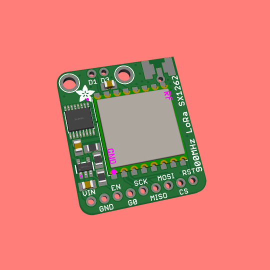
The SX1262 is an updated LoRa chip, so we made a breakout 📡🔧🔄
We got a hot tip to check out the Semtech SX1262 (https://www.digikey.com/short/504bpwww) - compared to our classic SX127x series of "RadioFruit" boards (https://www.adafruit.com/product/3072) the '1262 has lower power usage and longer range as well as some more options for spread-spectrum and extra modulation protocols. Most folks will probably use it for LoRa / LoRaWAN. The pinout is slightly different, so a few changes were made to the classic PCB. We also had some extra room, so we tossed in mounting holes. With this design, you can use wire, uFL, or SMA antennas - just solder whichever connector you desire. Note that the new chips are not software-compatible, so some driver tweaks will be needed to make it work. Coming soon.
#adafruit#lora#semtech#sx1262#longrange#lowpower#wirelesscommunication#radiotechnology#pcbdesign#antennadesign#iotdevices
8 notes
·
View notes
Text
just ordered parts for a rough draft of a bug sweeper /o/
turns out it’s not that complex of an idea. just a spectrum analyzer and a highly directional antenna really. the key issue i’m expecting is designing an antenna array that covers the full bandwidth of interest. the tinySA covers 100k-5.3G, which is pretty broad and definitely too much for most antennas. the spiral antenna design looks promising though, especially if it could be done in a PCB, but it may still end up being pretty large to accommodate freqs down to 100 kHz. maybe a pair of a spiral plus something else more compact for low freqs will work better
2 notes
·
View notes
Text
New from RAK
Custom-build antennas for perfect performance
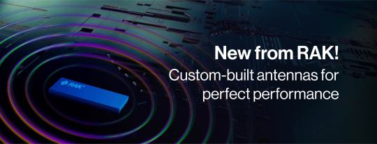
Have you ever had trouble finding the right antenna for your IoT device or project? With RAKwireless’ new service, you can now customize your antenna to maximize the performance of your products.
We offer custom antenna design, whether you’re using a product RAK has built from the ground up or looking to integrate a RAK antenna with your own designs.
The antenna is an integral part of wireless communication products as a whole and must be considered in the design to ensure optimal performance. A good antenna provides sufficient range, so a product or service can have a meaningful application.
However, there are many factors that impact antenna performance. By optimizing antenna parameters—such as gain, matching, bandwidth, size constraints, etc.—we’re able to provide the best range possible for the end product. We can serve any use case scenario: smart metering, asset tracking, transportation, smart agriculture, and more.
You may want to customize your antenna if:
Your product design is size constrained and you are struggling to balance dimension with antenna performance. You need good RF performance, but don’t want to make the product bulky.
You are using an off-the-shelf PCB antenna that you integrated in your pre-designed enclosure and are suffering bad RF performance.
You are in the product design stage and need help integrating a custom antenna in your package.
Let us know in the survey below what common antenna issues you’re experiencing, and whether they occur during the product design stage or post-production.
2 notes
·
View notes
Text
PCB Design Software Market 2023-2029: Growth Trends and Future Outlook
A programme that allows user to build a circuit layout for an electronic device is known as printed circuit board design software. Other elements include resistors, diodes, integrated circuits (ICs), and capacitors. PCB devices are used when small antenna elements cannot be attached to a breadboard. Businesses can utilise the technology to evaluate and examine the circuit's operations.
0 notes
Text
Choosing the Right RF Cable Assemblies for Your Communication Needs
RF (Radio Frequency) cable assemblies are critical components in communication systems, connecting RF devices including antennas, transmitters, receivers, and other equipment. Choosing the correct RF cable assembly is critical for preserving signal integrity, avoiding losses, and assuring consistent performance across a variety of applications. Here's a detailed guide that will help you navigate the selecting process properly.
1. Understanding RF Cable Assembly Types: RF cable assemblies are classified based on their intended application and frequency range. Common varieties include RG-58, RG-174, and RG-316 coaxial cables, as well as semi-rigid and flexible coaxial assemblies. Coaxial cables can transport high-frequency signals with low loss, making them excellent for applications that require efficient signal transmission over long distances. Semi-rigid cables provide excellent shielding and signal integrity, but require bending tools to install. Flexible coaxial assemblies are versatile and easy to install, making them ideal for applications that require wire routing flexibility.
2. Consider the frequency range and power handling capabilities of the RF cable assembly to meet your communication needs. Different cable types and assemblies are designed to function in specific frequency ranges, which range from a few megahertz to many gigahertz. Ensure that the cable assembly you select can meet the frequency needs of your RF devices without signal degradation or interference. Similarly, check the power rating of the cable assembly to ensure it is compatible with the power levels produced or communicated by your device.
3. Connector Compatibility and Interface: RF cable connectors ensure secure and dependable connections between devices. Common RF connectors include SMA, N-type, BNC, TNC, and DIN connectors, each with its own frequency range, impedance matching, and environmental resilience. To avoid signal loss and for best performance, make sure the connections on the cable assembly match the connectors on your RF devices. Consider connection gender (male or female), mounting type (cable mount, panel mount, or PCB mount), and interface requirements to ensure seamless integration with your communication system.
4. Environmental Considerations: Consider the environment in which the RF cable assembly will be installed. Outdoor installations may necessitate cables with weatherproofing features such as UV-resistant jackets, waterproof connectors, and corrosion-resistant materials to withstand exposure to elements such as rain, humidity, and temperature changes. Indoor applications may benefit from cables with flexible, flame-resistant jackets that meet safety and building regulations. Choosing cable assemblies suited for appropriate climatic conditions assures long-term reliability and endurance in your communication infrastructure.
5. Choose RF cable assemblies from recognized suppliers to ensure quality and reliability. Premium materials and manufacturing procedures are used to build high-quality assemblies, ensuring consistent performance and durability in harsh environments. Look for certifications and conformance with industry standards (such as MIL-STD, IEC, and RoHS) to ensure the cable assemblies' quality and reliability. Investing in durable cable assembly reduces downtime, maintenance costs, and potential signal difficulties, assuring continuous communication and operational efficiency.
6. Consider customization possibilities and technical support from the manufacturer or supplier when choosing RF cable assembly. Some applications may necessitate bespoke cable lengths, connector designs, or additional shielding to satisfy specific performance requirements. Work together with RF technical professionals to discuss your modification requirements and guarantee that the cable assemblies you select are tailored to your communication system's specific demands.
Choosing the proper RF cable assembly necessitates a careful consideration of cable types, frequency compatibility, connector interfaces, environmental suitability, quality requirements, and customization choices. Understanding these critical considerations, as well as working with RF engineering professionals or vendors, will allow you to confidently select cable assemblies that optimize signal transmission, dependability, and overall performance in communication applications.
0 notes
Text
Tips to design High Frequency PCB for optimal performance
Best Practices for High-Frequency PCB Design
We all know the importance of military electronic devices like military radars, satellite systems, communications, etc, for the safety of our country. But do you know that these systems consists of high-frequency Printed Circuit Boards? Therefore, a high-frequency printed circuit board (PCB) requires careful design to guarantee the best performance. As a PCB producer or user, you must know that even little errors can have a big effect on performance.
Here, in this insightful blog, we will discuss negotiating the challenges of high-frequency PCB design so that your product development project performs as intended.
Understanding the Basics
It is essential to understand why high-frequency PCBs need particular care before going into the details. Signals can deteriorate at high frequencies for reasons including crosstalk, signal reflection, and impedance mismatches. PCB design guidelines are helpful in reducing these problems and guaranteeing the effective operation of your printed circuit board.
Key Design Considerations
These super-critical High-Frequency Printed Circuit Boards need several careful considerations at every stage, from the design to production. Here are some noteworthy points to keep in mind.
Material Selection
Maximizing the performance of your PCB starts with selecting the appropriate material. FR4, Rogers, or Teflon (PTFE) are common materials used in high-frequency PCBs and have distinct
advantages:FR4: Lower dielectric losses but more expensive
Rogers: Consistent high-frequency performance with reduced dielectric losses.
Teflon or PTFE: Excellent performance, yet processing is more difficult and costly.
Picking the right material will depend on the specifications and budget of your project.
Layer Stack-Up
Your PCB's layer stack-up affects signal integrity. Signal integrity is improved, and loop regions are reduced when power and ground planes are close to signal layers. With the balanced layer stacking, electromagnetic interference (EMI) can be reduced in high-frequency designs.
Impedance Control
High-frequency PCB design depends critically on maintaining constant impedance. Mismatched impedance often results in lost and reflected signals. Controlled impedance traces are computed using the material's dielectric constant, trace width, and height. There are tools and software accessible to assist you in creating and validating impedance-controlled traces.
Being one of the market leaders in the PCB manufacturing industry, we at PCB Power apply these considerations to produce advanced high-frequency printed circuit boards.
Practical Tips for High-Frequency PCB Design
Here are some simple yet effective practical tips that can improve your PCB performance.
Using Shorter Trace Lengths: A shorter trace length can help reduce signal deterioration. Long traces can function as antennas, absorbing noise and producing EMI problems. Reduce the distance high-frequency signals must travel over the PCB.
Avoid Sharp Bends: Impedance alterations and signal reflection are two effects of abrupt bends in traces. To maintain signal integrity, use 45-degree angles or gentle curves rather than 90-degree turns.

The Right Grounding: It takes a strong grounding plan. To reduce noise and performance enhancement, use a ground plane to give signals a return route. Narrow ground traces are to be avoided since they can cause inductance and lower signal quality.

Advanced Techniques:
With technological advancement, new and modern techniques are implemented for high-frequency printed circuit board manufacturing.
Via Placement
High-frequency signals can be impacted by parasitic inductance and capacitance. To reduce the effect, use vias sparingly and put them thoughtfully. Use several vias to disperse the current equally as needed.
Differential Pair Routing
Differential pair routing helps lower noise and crosstalk for fast signals. Signal integrity must be preserved by routing differential pairs closely together with identical lengths.

Testing and Validation
Test and validate your high-frequency PCB thoroughly after it is designed. Test impedance and signal integrity with Time Domain Reflectometry (TDR) and Vector Network Analyzers (VNA). Furthermore, simulation software is highly useful for predicting PCB performance under different circumstances.
FINAL WORDS:
High-frequency printed circuit board design calls for meticulous attention to detail and following particular PCB design standards. High-frequency applications can be optimized on your PCB by choosing the appropriate materials, keeping impedance control, and putting in place efficient grounding and routing techniques. To be sure your design satisfies performance objectives, never forget the need for extensive testing and validation.
By using these tips, you can confidently take on the difficulties of high-frequency PCB design and guarantee that your projects meet the best possible performance and dependability criteria.
To learn more about printed circuit boards, please visit our resource page. Connect with us through [email protected] or call us at +1(818)8868900.
This Blog Originally Posted Here: Tips to design High Frequency PCB for optimal performance
0 notes
Text

Aluminum Nitride Ceramic PCB
Aluminum Nitride (AlN) is currently the best ceramic substrate material accessible. Its properties of high thermal conductivity (170 W/mK) combined with being a strong dielectric and a low expansion rate (CTE) make it the material of choice today as a substrate or package for high-power LEDs, ICs, sensors and many other components and circuits.
Reasons why you should choose Aluminum Nitride PCB for your project
Aluminum Nitride (AlN) PCBs offers several compelling reasons, especially in applications where thermal management, high-frequency performance, and reliability are critical. Here are some key reasons to consider using AlN PCBs:
·Exceptional Thermal Conductivity: AlN ceramics have excellent thermal conductivity properties, making them highly effective at dissipating heat generated by electronic components. This property is crucial for maintaining component reliability, extending the lifespan of electronics, and preventing overheating-related failures.
·High-Frequency Performance: AlN PCBs exhibit low signal loss and minimal signal distortion, making them well-suited for high-frequency and microwave applications. They provide reliable signal transmission and are ideal for RF (Radio Frequency) circuits, microwave antennas, and advanced communication systems.
·Electrical Insulation: AlN ceramics possess excellent electrical insulation properties. They have a high dielectric strength, preventing electrical leakage and ensuring the isolation of electrical components and signals. This insulation is essential for maintaining signal integrity and preventing unintended electrical connections.
·Mechanical Strength: AlN ceramic substrates have good mechanical strength, with the ability to withstand mechanical stresses during manufacturing, assembly, and operation. This mechanical robustness contributes to the overall reliability of electronic systems.
·Compatibility with Semiconductor Devices: The thermal expansion coefficient of AlN is relatively close to that of silicon, a common material used in semiconductor devices. This compatibility allows for efficient heat transfer from semiconductor components, reducing the risk of thermal stress and enhancing their performance and longevity.
·High-Power and High-Temperature Applications: AlN PCBs are well-suited for high-power electronic components and high-temperature environments. They can efficiently dissipate heat from power amplifiers, voltage regulators, LEDs, and other heat-generating devices.
·Longevity and Reliability: The superior thermal management provided by AlN PCBs contributes to the longevity and reliability of electronic systems, reducing the risk of premature component failures due to overheating.
·Wide Range of Applications: AlN PCBs find application in various industries, including aerospace and defense, telecommunications, medical devices, automotive, and industrial electronics. They are versatile and suitable for demanding electronic applications.
·Customization: AlN PCBs can be customized to meet specific design requirements, including layer count, dimensions, and design layout, ensuring that they are tailored to the needs of the application.
·Efficient Heat Dissipation: The exceptional heat dissipation properties of AlN PCBs allow for the effective management of thermal issues without the need for additional cooling mechanisms, such as heat sinks or fans.
In conclusion, choosing Aluminum Nitride (AlN) PCBs offers lots of advantages, including superior thermal conductivity, high-frequency performance, electrical insulation, and mechanical strength. These properties make them a preferred choice in applications where traditional PCB materials may not meet the stringent requirements for thermal management and reliability. At Hitech Circuits, we supply both Aluminium Nitride PCB (AlN) processed by thick film process (Silver/silver palladium metalization) as well as Direct Plated Copper Technologies (DPC), with copper tracks and pads.
#AINPCB #ceramicpcb
0 notes
Text
The Evolution of System in Package: Past, Present, and Future

The Genesis of System in Package Technology
In the early days of electronics, the industry was dominated by single-function components. Each transistor, resistor, and capacitor had its place on a printed circuit board (PCB), contributing to the overall function of the device. However, as technology advanced and devices became more complex, this approach proved increasingly inefficient. The advent of integrated circuits (ICs) in the 1960s marked a significant leap forward, but even these had limitations. The need for greater integration and miniaturization led to the birth of system in package (SiP) technology.
SiP technology emerged in the 1980s as a revolutionary concept that allowed multiple ICs to be integrated into a single package. This innovation enabled the development of more compact and efficient electronic devices. Initially, SiP was used in niche applications, such as military and aerospace, where the high cost was justified by the need for performance and reliability. As the technology matured, costs decreased, and SiP became viable for consumer electronics, paving the way for the miniaturized gadgets we use today.
The Golden Age of System in Package: Present Innovations
Today, System in Package technology is at the forefront of electronics design, driving innovations in various industries. Transitioning from the past, the present state of SiP showcases its capabilities in smartphones, wearables, and IoT devices. Modern SiP solutions integrate not just ICs, but also passive components, sensors, and antennas, all within a single package. This level of integration has enabled unprecedented levels of functionality in increasingly smaller form factors.
One of the key benefits of contemporary SiP technology is its ability to support heterogeneous integration. By combining different types of components, such as analog, digital, RF, and power management ICs, SiP can deliver complex functionalities that would be difficult to achieve with traditional PCB designs. Moreover, the use of advanced packaging techniques, such as through-silicon vias (TSVs) and flip-chip bonding, enhances the performance and reliability of SiP assemblies.
In the consumer electronics sector, SiP has been instrumental in the development of compact and powerful devices. For instance, the latest smartphones utilize SiP to integrate multiple communication protocols, processing units, and sensors, all while maintaining a slim profile. Similarly, wearable devices like smartwatches benefit from SiP by incorporating a variety of sensors, processors, and communication modules in a tiny footprint.
Future Horizons: The Next Frontier for System in Package
Looking ahead, the future of System in Package technology promises even greater advancements and possibilities. The relentless drive towards miniaturization, coupled with the growing demand for high-performance computing and connectivity, will push SiP to new heights. Emerging trends such as 5G, artificial intelligence (AI), and the Internet of Things (IoT) will heavily rely on the capabilities of SiP to meet their stringent requirements.
One of the most exciting prospects for SiP is its potential role in enabling advanced AI applications. As AI algorithms become more complex and data-intensive, the need for efficient and high-performance hardware solutions becomes paramount. SiP can provide the necessary integration of processing units, memory, and specialized AI accelerators in a compact form factor, making it ideal for edge computing devices and smart sensors.
Furthermore, the integration of photonic components within SiP is another promising development on the horizon. Photonic SiP, which incorporates optical components for high-speed data transmission and processing, could revolutionize telecommunications and data centers. This approach would address the bandwidth and latency challenges posed by the ever-increasing data demands of modern applications.
The continued evolution of manufacturing techniques will also play a critical role in the future of SiP. Advances in 3D packaging, wafer-level integration, and novel materials will enable even higher levels of integration and performance. These innovations will not only enhance the capabilities of SiP but also make the technology more accessible and cost-effective for a broader range of applications.
System in Package: Bridging the Gap Between Past, Present, and Future
In conclusion, the journey of System in Package technology from its nascent stages to its current prominence and future potential is a testament to the relentless innovation in the electronics industry. The transition from discrete components to highly integrated SiP solutions has transformed the landscape of electronic device design, enabling the development of smaller, more powerful, and more efficient products.
As we look to the future, the role of SiP will only become more critical in addressing the challenges of modern technology. From supporting the proliferation of 5G networks and AI applications to pushing the boundaries of miniaturization and performance, system in package technology is poised to remain at the heart of the next wave of electronic innovations. With each new advancement, SiP continues to bridge the gap between past achievements and future possibilities, shaping the world of electronics in ways we can only begin to imagine.
1 note
·
View note
Text

Applications of Flex PCB
1 Consumer electronics
Flex PCBs enable the production of foldable smartphones, tablets, and other electronic devices. It has high durability and flexibility. These foldable gadgets are widely used in today’s world. Because of their flexibility and lightweight construction, they are used highly for wearable electronics. They can be sewn into garments or worn as elastic bands.
2 Medical Equipment
Applications like Endoscopes use flexible circuits, which allow for compact designs and easy transit through the body’s cavities. Flex PCBs are commonly used to make medical wearables like health monitoring gadgets and smart medical patches.
3 Automotive sector
Flex PCBs are used in the interior of automotive industrial which includes flexible dashboard displays, sensors in the seat, and numerous other components. By using flex PCBs here will utilise the space effectively. They are also implemented in sensors, control systems, and lighting applications that require flexibility for installation in limited places.
4 Aerospace and Defence
Flex PCBs are employed in satellite systems where weight, space, and dependability are important factors. The flexibility enables easy integration into small places within the satellite. Flex PCBs are frequently utilized in military equipment, including aircraft and communication systems, due to their ability to endure vibrations, shocks, and severe weather conditions.
5 Industrial Automation
Flex PCBs can be implemented in a variety of industrial sensors, control systems, and automation applications that require compact design and reliable performance. They are also integrated into robotic systems to provide the flexibility required for the robotic joint movement and congested routing in places which are tight.
6 Communication Devices
The adaptability of flex PCBs is useful in building conventional antennas and devices for communication. They will provide improved signal reception for the antennas. To achieve sleek designs, Flexible PCBs are used in smartphones as well as other mobile devices.
7 LED Lights
Flex PCBs are often used in flexible LED strips because they are easily bendable and conformable to various shapes. This is beneficial for both ornamental lighting and architectural applications.
8 Innovative Displays
Nowadays, TV screens are a lot more curved than often. This is implemented in TVs for the best experience for Cinemas, sports or even web series for the audience. This is achieved by using Flex PCBs in order to occupy the space effectively.
0 notes
Link
1 note
·
View note
Text
Notable activities of the Electronics and Communication Engineering department
Notable activities of the Electronics and Communication Engineering department
In 2010, K.Ramakrishnan College of Technology (KRCT) founded the Department of Electronics and Communication Engineering (ECE), which attained NBA accreditation in 2020, reaffirming its dedication to excellence. In 2023, the Department successfully underwent re-accreditation, reaffirming its sustained dedication to quality education. Further, the department offers a wide range of courses and equipped with research laboratories. Also, the department provides students with a holistic learning experience, preparing them to excel in the dynamic field of electronics and communication.
Courses Offered
In fact, the department of Electronics and Communication Engineering at KRCT offers a range of courses providing students with comprehensive learning opportunities.
В.Е. (ECE)
M.E. (VLSI Design)
Ph.D. (ECE) - Full Time/Part
Research Laboratories
Above all, The Department of Electronics and Communication Engineering boasts state-of-the-art research laboratories, developing an environment conducive to innovative research and practical learning experiences.
The Intel Intelligence Lab
National Instruments Lab, and
RF & Antenna Design Lab,
Electronics and Communication Engineering: 2023 Jan – March Quarterly Events Conducted
Audits
Firstly, Key deliverable audit conducted by CC coordinator of Allied courses Domain on 18.01.2023. Also, CDP, CAP and CAM were verified and approved by CC Coordinator.
At the same time, Key deliverable audit conducted by CC coordinator of Applied Electronics Domain on 18.01.2023.CDP, CAP and CAM were verified and approved by CC Coordinator.
Further, the key deliverable audit for II Year subjects was conducted by the Course Committee Coordinator.
For the Communication Domain, Dr. S. Suganthi, Professor of ECE, oversaw the audit for the subject "ETW."
In the Applied Electronics Domain, Dr. M. Kavitha, Professor of ECE, led the audit for the subjects "Control Systems" and "Analog Circuits."
Campus Activities
Alumni Interaction with final year placed students by Mr.Lakshman raj of (2012-2016) batch on 24.01.2023. The event was successfully organized and conducted by Ms.S.Geerthana AP/ECE /Alumni coordinator.
Students of ECE participated and exhibited their talents in 74th Republic Day parade on 26.01.2023 organized by KRGI.
Faculty members and students of the ECE department came together to plant saplings in observance of National Science Day.
A seminar and hands-on practice session on PCB design and fabrication were conducted for the II-year ECE A section students.
Insightful Talks at Electronics and Communication Engineering Department
Mr. S. Amarnath and Mr. S. Bharath from the III Year shared the insights they gained during the Ideation Camp of TNSI-2023, organized at University College of Engineering, BIT Campus.
On February 23, 2023, Mr. V. Ramkumar, Assistant Professor in the Department of ECE, delivered a value talk on Project Deliberation to the students of III/ECE.
An Invited Talk on "Career Opportunities in Multi-National Companies" was delivered by Mr. G. Dinesh, an Automation Test Engineer at Wipro Technologies, Chennai. Mr. Dinesh, an alumnus from the 2013-2017 batch, shared insights and experiences regarding career paths and opportunities in multinational companies.
Participations/Innovations
Students from III/ECE and II/ECE visited Kerala Electrical and Allied Engineering Co.Ltd. on both March 4, 2023, and March 11, 2023. During these visits, students acquired valuable knowledge on general engineering concepts, including the intricacies of coil winding in transformers.
Also, on March 21, 2023, students of III ECE presented their idea pitch for Olimayam 2.0 KIT.
Furthermore, students of ECE showcased their innovation at the CSA conference.
In addition, students of ECE attended a Boot Camp at KIOT organized by Olimayam 2.0.
Seminars
Additionally, The Department of ECE, Institution of Engineers, in collaboration with the NDLI club at KRCT, organized a seminar on "Structural Integrity Evaluation using Electrical Strain Gauge Sensor." The event was presided over by Dr.N.Raju, Additional General Manager at Bharat Heavy Electricals Limited (Public Sector).
Moreover, The Institute of Engineers Student Chapter, in collaboration with KRCT NDLI Club and the National Digital Library of India Club, organized a seminar on "Introduction to System C and Its Career Opportunities in the Semiconductor Industry" on March 31, 2023.
Faculty Success
Above all, Dr.V.Ramkumar, Assistant Professor in the Department of ECE, successfully defended his thesis and completed his Ph.D. viva voce examination.
To Conclude
Thus, the Department of Electronics and Communication Engineering at KRCT represents excellence. Further, through insightful talks, participation in seminars, workshops, and campus activities, as well as faculty successes, the department continues to inspire and empower students, preparing them to become future-ready engineers. Moreover, the department remains committed to nurturing talent, research, and contributing positively to societal and industrial advancements in the field of electronics and communication engineering.
https://krct.ac.in/blog/2024/05/25/notable-activities-of-the-electronics-and-communication-engineering-department/
#krct the top college of technology in trichy#quality engineering and technical education.#krct the best college of technology in trichy#k ramakrishnan college of technology trichy#Notable activities of the Electronics and Communication Engineering departmen#research publication in ece#ece in krct#election result in krct#ai college
0 notes
Text
Small, Fast, Slower Than Qi Android 15 NFC Wireless Charging
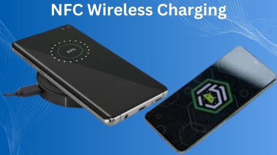
Although NFC wireless charging is slower than Qi wireless charging, Android 15 may support it because fewer hardware is needed.
Qi wireless charging coil
When a smartphone has wireless battery charging capabilities, the Qi standard is usually used. Future Android 15-capable smartphones, however, might feature NFC Wireless Charging, which offers an alternative method of wireless charging. In any case, whether or not this method is less efficient than the Qi standard, Google appears to be working on finding a way to integrate this technology into models that are supported.
NFC wireless charging is perfect for small smartphones since it requires less hardware to function
For Qi-enabled devices with larger wireless charging coils, NFC Wireless Charging may overcome this problem using contactless payment technologies. Despite its May 2020 debut, NFC Wireless Charging (WLC) has not received significant use. Its slower charging speeds than Qi may explain this. Flexible charging antennae fit wireless earbuds, Bluetooth trackers, smart watches, and more. They can be 1 cm.
With the anticipated release of Android 15 later this year, NFC wireless charging
Android 15
Compatibility and an influx of WLC enabled accessories could be seen. The NFC APIs of the operating system now support WLC, according to Missal Rahman of Android Authority, who also claims that the Android 15 beta 1 has these features. According to the article, Google made an attempt to implement WLC support in late 2021 nearly a year and a half after the standard was initially published but eventually shelved all of her plans.
Google did not provide a reason for why it would revive its shelved project, but other goods like Bluetooth trackers which can be coupled with an Android phone could also benefit from this inclusion, in addition to small smartphones. These trackers and other accessories would be easy to maintain and charge with the integration of NFC wireless charging.
But integrating support into software is one thing; adding it as a feature to other items is quite another. Hopefully, additional information on this will be provided at the forthcoming I/O keynote.
There may be a new wireless charging feature for Android 15 devices.
Android is going to introduce NFC wireless charging functionality for your devices.
Wireless charging usually conjures up the Qi standard. Qi wireless charging is embedded into many everyday smart devices.
It has been around for a long.
However, Qi wireless charging is either rare or nonexistent for a large number of smaller electronic gadgets.
This is due to the possibility that smaller devices lack the internal space necessary to accommodate a coil large enough to receive enough power.
The industry group that promotes Near Field Communication (NFC), which enables contactless payments, created the NFC Wireless Charging (WLC) protocol.
NFC wireless charging, introduced in May 2020, employs far smaller antennas than Qi. NFC wireless charging antennas are designed to fit into minuscule smart devices such as tracker tags, smartwatches, styluses, and earphones. They are packaged in a bending, flexible PCB and can be smaller than 1cm. To save even more space, the same antenna can also be utilized for conventional NFC data transfers. It would be logical to replace the NFC chip used in many smaller, low-power devices (such as tracker tags) that handles basic data transfers with a single antenna that handles charging and communication.
NFC wireless charging was introduced about four years ago, however it is still not widely used in many consumer goods. Major operating systems like Android may not support all platforms, which could be one cause for that. However, NFC Wireless Charging will soon be supported by the forthcoming Android 15 version, which may open the door for a large number of WLC-capable accessories to become available.
Android NFC Wireless Charging
We saw that Google made considerable changes to the NFC stack of the operating system when it published Android 15 beta 1 last week. For instance, a class named NFC Charging is now included in the system app that manages NFC-related events; it can read the charging information payloads received via NFC, initiate and stop NFC charging, and perform other functions. While the class mentions “version 1.0.0,” this most likely alludes to Android’s initial NFC Charging implementation, not WLC 1.0 (to put things in perspective, the NFC Forum revealed WLC 2.0 in late 2021; the only difference is that WLC 2.0 enables even lower antenna sizes).
WLC-related enhancements to the operating system’s NFC APIs which aren’t yet available in AOSP are also included in Android 15 beta 1. It’s notable that Google gave up on its initial attempt to add WLC support in late 2021, over a year and a half after the standard was originally made public. However, Google seems to have rekindled interest in adding WLC support to Android earlier this year, so why now?
Tracker tags may be one fascinating use for NFC wireless charging. In addition to having tiny batteries that don’t need much power to recharge (WLC can send up to 1W of electricity over a distance of 2cm) and already having NFC chips so they can transmit information about their owner to anyone discovers them, tracker tags are frequently too thin to contain a Qi wireless charging coil. While some tracker tags contain non-rechargeable batteries, several already tout up to a year of battery life, such as those that work with Android’s Find My Device network. It would be easier to charge and less expensive to maintain future tracker tags if they supported NFC wireless charging.
Stylus charging represents an additional possible use case. As NFC Wireless Charging is really built into the USI 2.0 specification, NFC charging is already possible for USI 2.0 styluses that are now available on the market. But in order to charge them, you’ll still need an NFC charging transmitter-equipped compatible device.
Hopefully, wireless charging will be more common in smaller gad gets like earbuds, styluses, smartwatches, and tracker tags once NFC Wireless Charging functionality is integrated into Android.
Read more on Govindhtech.com
0 notes
Text
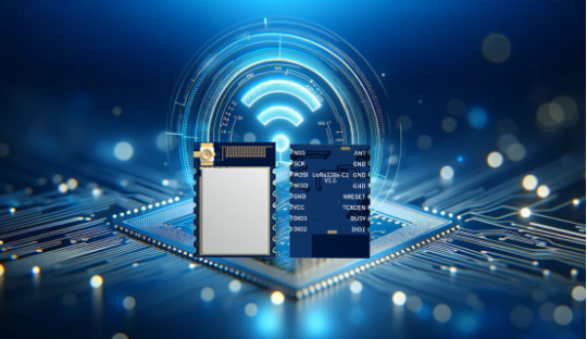
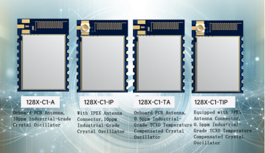
LoRa128X-C1 Series: High Sensitivity 2.4GHz, IPEX/PCB antenna, Long Range LoRa Modules
The LoRa128X-C1 series is a set of advanced modules designed to meet the diverse needs of modern wireless communication applications. Users can choose from four different models - LoRa128X-C1-TIP, LoRa128X-C1-IP, LoRa128X-C1-TA, and LoRa128X-C1-A - to select the module that best suits their specific requirements.
Applications :
The LoRa128X-C1 series is highly suitable for a wide range of applications, including wireless remote controls, smart home devices, toy control, tire pressure monitoring, health monitoring, and tag readers and writers.
Model Overview:
LoRa128X-C1-A: Features an onboard PCB antenna and a 10ppm industrial-grade crystal oscillator, providing a balance between performance and economy.
LoRa128X-C1-IP: Equipped with an IPEX antenna base and a 10ppm industrial-grade crystal oscillator, offering high cost-effectiveness and efficient operation.
LoRa128X-C1-TA: Comes with an onboard PCB antenna and a 0.5ppm industrial-grade TCXO, ensuring reliable and accurate communication.
LoRa128X-C1-TIP: Features an IPEX antenna base and a 0.5ppm industrial-grade TCXO temperature-compensated crystal oscillator, ensuring precise and stable performance.
Main features:
Operating frequency range: 2400-2500 MHz.
Modulation modes: LoRa, FLRC, and FSK modulation.
Data transfer rate: 0.476-202 Kbps under LoRa modulation.
Maximum Output power: 12.5dBm.
Sensitivity: -132dBm under LoRa modulation.
Accuracy: High precision crystal oscillator (0.5ppm TCXO/10ppm).
Communication: Packet communication mode, with 256 bytes of receive and transmit FiFo.
Operating Voltage range: 1.8-3.7 V.
Operating Temperature range: -40 to +85°C.
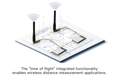
The LoRa128X-C1 series LoRa modules are produced and tested using lead-free processes, compliant with RoHS and REACH standards, ensuring not only environmental friendliness but also high quality and reliable performance. Based on Semtech's original SX1280/SX1281 RF chip, these modules utilize LoRa modulation to overcome the limitations of traditional 2.4GHz modules in terms of communication distance. Additionally, they integrate the "time of flight" function for wireless distance measurement applications.
With the high penetration performance of the 2.4GHz frequency band and LoRa mode, the LoRa128X-C1 series has very high receiving sensitivity and strong environmental anti-interference capability, making it very suitable for situations requiring long-distance 2.4GHz transmission. Choose the LoRa128X-C1 series LoRa modules as part of your next project and experience the excellent performance and versatility it offers in the field of wireless communication.
For details, please click:https://www.nicerf.com/products/
Or click:https://nicerf.en.alibaba.com/productlist.html?spm=a2700.shop_index.88.4.1fec2b006JKUsd
For consultation, please contact NiceRF (Email: [email protected]).
0 notes
Last Seen Blogs

buruksiirler-blog
Hercai.

m3xyuu
M3XYUU

srsumon
S R Sumon

bloghhhhhhfu
Untitled

meanbeanzone
MEAN BEAN