#Global SEmiconductor Wafer Polishing and Grinding Equipment Market
Explore tagged Tumblr posts
Visit Tumblr Blog
Explore Tumblr blogs with no restrictions, modern design and the best experience.
Last Seen Tumblr Blogs


Fun Fact
When “GIF” was named word of the year in 2012, Oxford Dictionaries U.S.A. credited Tumblr for pushing the word.
Text
Semiconductor Wafer Polishing and Grinding Equipment Market: Trends and Insights
Market Overview
The Semiconductor Wafer Polishing and Grinding Equipment Market is expected to register a CAGR of 4.1% during the forecast period. The global semiconductor wafer polishing and grinding equipment market has been witnessing steady growth, driven by the rising demand for miniaturized electronic devices and advanced semiconductor fabrication technologies. The increasing adoption of System-on-Chip (SoC), microelectromechanical systems (MEMS), and advanced packaging techniques has further propelled market expansion.
Key Market Drivers
Surging Demand for Consumer Electronics – The proliferation of smartphones, laptops, smart devices, and IoT-connected appliances fuels the need for high-performance semiconductors.
Growth in AI and 5G Technologies – AI-driven applications and the widespread deployment of 5G networks demand sophisticated semiconductor chips, boosting the need for precision wafer processing.
Advancements in Semiconductor Manufacturing – The shift towards 3D ICs, FinFET technology, and smaller node sizes (7nm, 5nm, and beyond) has necessitated advanced wafer grinding and polishing techniques.
Rising Demand for Automotive Electronics – The increasing use of semiconductor-based sensors, processors, and controllers in electric vehicles (EVs) and autonomous vehicles contributes to market growth.
Increase in Foundry Investments – Leading semiconductor manufacturers such as TSMC, Samsung, and Intel are heavily investing in new fabrication plants, further driving the demand for wafer processing equipment.
Market Segmentation
The market is segmented based on equipment type, wafer size, application, and geography.
1. By Equipment Type
Wafer Grinding Equipment – Used for thinning wafers to the desired thickness for different applications.
Wafer Polishing Equipment – Ensures smooth surfaces and removes defects to improve wafer quality.
CMP (Chemical Mechanical Polishing) Equipment – Provides a hybrid polishing approach for high-precision semiconductor processing.
2. By Wafer Size
150mm Wafers
200mm Wafers
300mm Wafers (Dominant segment) – Most advanced semiconductor production relies on larger wafer sizes to improve yield and efficiency.
3. By Application
Memory & Logic ICs – Used in computing and data storage applications.
Power Devices – Essential for energy-efficient systems in electric vehicles and renewable energy applications.
MEMS & Sensors – Integral to industrial automation, healthcare, and smart consumer electronics.
Optoelectronics – Widely used in LED, laser, and photonic applications.
4. By Geography
North America – Leading due to strong semiconductor industry players like Intel, AMD, and Qualcomm.
Asia-Pacific (Largest Market) – Driven by semiconductor giants in Taiwan, South Korea, and China.
Europe – Growing demand for automotive and industrial semiconductor applications.
Rest of the World – Emerging semiconductor manufacturing hubs in the Middle East and Latin America.
Industry Challenges
Despite strong growth, the industry faces several challenges:
High Capital Investment – The cost of wafer polishing and grinding equipment is significant, impacting smaller semiconductor manufacturers.
Technological Complexity – Achieving ultra-thin wafers without defects requires advanced and precise equipment.
Supply Chain Disruptions – Semiconductor shortages and geopolitical factors affect the availability of raw materials and machinery components.
Stringent Regulatory Standards – Environmental regulations around chemical usage in polishing and grinding processes require manufacturers to adopt sustainable practices.
Market Trends and Innovations
Automation & AI Integration – Adoption of AI-driven predictive maintenance and automation in wafer processing to enhance efficiency.
Sustainable Manufacturing – Development of eco-friendly CMP slurries and water-recycling systems to reduce environmental impact.
Hybrid Processing Techniques – Combination of CMP and mechanical polishing to improve wafer uniformity and precision.
Emergence of 450mm Wafers – Although still in development, larger wafer sizes could revolutionize semiconductor production.
Future Outlook
The semiconductor wafer polishing and grinding equipment market is poised for sustained growth, driven by ongoing technological advancements and the increasing need for high-performance semiconductors. With strong investments in semiconductor fabrication plants and growing demand for AI, 5G, and automotive electronics, manufacturers are expected to prioritize innovation in wafer processing solutions.
Companies investing in automation, sustainable practices, and precision technologies will likely gain a competitive edge in this evolving industry. The future of semiconductor manufacturing will depend on how efficiently companies can scale up production while maintaining wafer quality and sustainability.
Conclusion
The semiconductor wafer polishing and grinding equipment market is an integral part of the rapidly expanding semiconductor industry. As demand for smaller, more efficient, and powerful semiconductor chips continues to grow, advancements in wafer processing technology will play a crucial role in shaping the future of electronics. By addressing industry challenges and leveraging cutting-edge innovations, market players can capitalize on the tremendous growth opportunities in this sector. For a detailed overview and more insights, you can refer to the full market research report by Mordor Intelligence. https://www.mordorintelligence.com/industry-reports/semiconductor-wafer-polishing-and-grinding-equipment-market
#Semiconductor Wafer Polishing and Grinding Equipment Market#Semiconductor Wafer Polishing and Grinding Equipment Market size#Semiconductor Wafer Polishing and Grinding Equipment Market share#Semiconductor Wafer Polishing and Grinding Equipment Market trends
0 notes
Photo

SEmiconductor Wafer Polishing and Grinding Equipment Market Trends, Key Players, Overview, Competitive Breakdown And Regional Forecast By 2026 | TOKYO SEIMITSU CO., LTD, Logomatic GmbH, Komatsu NTC
Get Free Sample Copy of SEmiconductor Wafer Polishing and Grinding Equipment Market Report @ https://bit.ly/3nc7sY4
#SEmiconductor Wafer Polishing and Grinding Equipment Market Size and Share#Global SEmiconductor Wafer Polishing and Grinding Equipment Market#Semiconductors and Electronics
0 notes
Text
Growing Demand for Global Semiconductor Wafer Polishing and Grinding Equipment Market research to Significantly Increase Revenues Through 2026
Market Analysis: Global Semiconductor Wafer Polishing and Grinding Equipment Market
Global semiconductor wafer polishing and grinding equipment market is set to witness a substantial CAGR of 7.45% in the forecast period of 2019-2026. The report contains data of the base year 2018, historic year 2017. Increasing consumption of consumer electronics and rising outsourcing activities is another factor for the growth of this market.
Market Definition: Global Semiconductor Wafer Polishing and Grinding Equipment Market
Wafer is a thin piece of a semiconductor which is usually made of crystalline silicon which is mainly used as a base for the silicon based photovoltaic cell and to fabricate electronic integrated circuits. Today, thin wafers are more in demand as electronics are getting smaller and smaller with time. Grinding machine as the name suggest is a machine which is used for grinder. Belt grinder, cylindrical grinder, surface grinder, and bench grinder are some of the common type of grinder. Increasing usage of electronic device is the factor fuelling the growth of this market.
Get Sample Analysis of Global Market Information: https://www.databridgemarketresearch.com/request-a-sample/?dbmr=global-semiconductor-wafer-polishing-and-grinding-equipment-market
Market Drivers:
Rising demand for miniaturization of semiconductor will drive the market growth
Growing prevalence for consumer electronics also acts as a market driver
Increasing outsourcing activities will also propel the market growth
Availability of incentives and discounts for long term customer also contributes as a major factor in the growth of this market
Market Restraints:
High development cost acts as a restraining factor for the market growth
Problems associated with the manufacturing will also hamper the growth of this market
Segmentation: Global Semiconductor Wafer Polishing and Grinding Equipment Market
By Equipment
Deposition
Lithography
Ion Implant
Etching and Cleaning
Others
By End- Users
Foundries
Memory Manufacturers
IDMs
Others
By Geography
North America
Europe
Asia-Pacific
South America
Middle East and Africa
U.S.
Canada
Mexico
Germany
Italy
U.K.
France
Spain
Netherlands
Belgium
Switzerland
Turkey
Russia
Rest of Europe
Japan
China
India
South Korea
Australia
Singapore
Malaysia
Thailand
Indonesia
Philippines
Rest of Asia-Pacific
Brazil
Argentina
Rest of South America
Saudi Arabia
UAE
South Africa
Egypt
Israel
Rest of Middle East and Africa
Get TOC of Full Report: https://www.databridgemarketresearch.com/toc/?dbmr=global-semiconductor-wafer-polishing-and-grinding-equipment-market
Key Developments in the Market:
In December 2018, Tokyo Big Sight announced the launch of their DFG8640 which is a fully automatic grinder compatible with 8”-diameter wafers which is very good for lithium tantalite, silicon, silicon carbide and lithium niobate. DFG8640 will help to improve the productivity and can achieve high-precision grinding through (1) optimizing the processing point layout
In November 2018, Applied Ventures, LLC, announced their new co-investment initiative with Empire State Development so that they can increase innovation in Upstate New York. The main aim is to invest in promising Upstate New York startups across different industries such as semiconductor, artificial intelligence, autonomous vehicles and others
Competitive Analysis
Global semiconductor wafer polishing and grinding equipment market is highly fragmented and the major players have used various strategies such as new product launches, expansions, agreements, joint ventures, partnerships, acquisitions, and others to increase their footprints in this market. The report includes market shares of semiconductor wafer polishing and grinding equipment market for Global, Europe, North America, Asia-Pacific, South America and Middle East & Africa.
Major Market Competitors/Players
Few of the major competitors currently working in the global semiconductor wafer polishing and grinding equipment market are Applied Materials, Inc., EBARA CORPORATION, Lapmaster, Entrepix, Inc., Revasum., TOKYO SEIMITSU CO., LTD, Logomatic GmbH, Komatsu NTC, OKAMOTO CORPORATION, Amtech Systems, Inc., BBS KINMEI CO.,LTD., DYMEK Company Ltd., Dynavest Pte Ltd., FUJIKOSHI MACHINERY CORP., G&N Genauigkeits Maschinenbau Nürnberg GmbH, Gigamat Technologies, Hunan Yujing Machinery Co., Ltd., Meyer Burger Technology AG, Speedfam (I) Pvt. Ltd., among others.
0 notes
Text
0 notes
Text
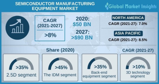
Semiconductor Manufacturing Equipment Market to Observe Rugged Expansion at a Top CAGR by 2027
The semiconductor manufacturing equipment market is anticipated to record notable growth by 2027 on account of soaring adoption of electric vehicles worldwide. In addition, increasing prevalence of IoT devices is set to drive market expansion over the forecast period.
Semiconductor manufacturing equipment refers to equipment that are typically used to produce semiconductor devices. Booming consumer demand for higher performing semiconductors has stimulated constant improvements in the technology employed in the products. Moreover, increasing focus on R&D activities to develop high-quality semiconductor manufacturing equipment to match the fast-paced progress in chip technology has fostered product outlook in recent years.
Get sample copy of this research report @ https://www.gminsights.com/request-sample/detail/4233
Furthermore, industry players are employing lucrative strategies to gain a competitive edge in the market, which has positively impacted the overall business landscape. For instance, in September 2021, Applied Materials, Inc., a key software, services, and equipment manufacturer for semiconductor devices, launched its novel products namely, the VIISta 900 3D hot ion implant system and the Mirra Durum CMP system.
The VIISta 900 injects ions while minimizing the damage caused to the lattice structure, thereby providing 40 times lesser resistivity as compared to a room temperature implant. Meanwhile, the Mirra Durum CMP system combines cleaning, polishing, drying, and material removal measurement in a single system to produce consistent wafers with the finest quality surfaces. Both products have been designed to assist silicon carbide (SiC) chipmakers in achieving 200mm production.
In another instance, in November 2020, ASML, a leading manufacturer of chipmaking equipment, completed the acquisition of Berliner Glas Group, a major manufacturing technology provider that specializes in optical systems. The deal enabled ASML to broaden its product portfolio and production capacity significantly.
The semiconductor manufacturing equipment market has been segmented on the basis of supply chain process, product, dimension, and region. With respect to product, the market has further been categorized into back-end equipment (test equipment, wafer manufacturing equipment, assembly & packaging equipment, and others) and front-end equipment (water surface conditioning equipment, lithography, polishing & grinding, and others).
Request for customization @ https://www.gminsights.com/roc/4233
Under back-end equipment, the assembly & packaging equipment segment is projected to amass substantial gains by 2027, progressing at a CAGR of approximately 7.0% over the forecast timeframe. Mounting demand for advanced packaging-based chipsets in consumer electronics products and connected devices is likely to bolster segmental growth over 2021-2027.
From the regional point of view, the LAMEA semiconductor manufacturing equipment market is expected to register around 6.0% CAGR through the analysis period to reach a sizable valuation by the end of 2027. Rising number of government initiatives supporting the development of the semiconductor manufacturing industry across LAMEA is estimated to boost regional market expansion over the following years.
Table of Contents (ToC) of the report:
Chapter 1 Methodology and Scope
1.1 Scope & definition
1.2 Methodology & forecast
1.3 Data Sources
1.3.1 Primary
1.3.2 Secondary
Chapter 2 Executive Summary
2.1 Semiconductor manufacturing equipment market 3600 synopsis, 2016 - 2027
2.1.1 Business trends
2.1.2 Regional trends
2.1.3 Product trends
2.1.4 Dimension trends
2.1.5 Supply chain process
Browse complete Table of Contents (ToC) of this research report @ https://www.gminsights.com/toc/detail/semiconductor-manufacturing-equipment-market
About Global Market Insights:
Global Market Insights, Inc., headquartered in Delaware, U.S., is a global market research and consulting service provider; offering syndicated and custom research reports along with growth consulting services. Our business intelligence and industry research reports offer clients with penetrative insights and actionable market data specially designed and presented to aid strategic decision making. These exhaustive reports are designed via a proprietary research methodology and are available for key industries such as chemicals, advanced materials, technology, renewable energy and biotechnology.
Contact Us:
Contact Person: Arun Hegde
Corporate Sales, USA
Global Market Insights, Inc.
Phone: 1-302-846-7766
Toll Free: 1-888-689-0688
Email:[email protected]
#Semiconductor Manufacturing Equipment Market Analysis#Semiconductor Manufacturing Equipment Market by Type#Semiconductor Manufacturing Equipment Market Share#Semiconductor Manufacturing Equipment Market Development#Semiconductor Manufacturing Equipment Market
0 notes
Text
Semiconductor Manufacturing Industry Research Report - Global Forecast to 2030
Global Semiconductor Production Equipment Market - Overview
The semiconductor production equipment market is garnering substantial traction across the globe. The market growth is attributed to rapid industrialization and economic growth. Besides, large technological advances in telemetry solutions and semiconductor products push the growth of the market. Information and communication industries worldwide are creating a significant demand for semiconductor production equipment. Moreover, rising usages of chips in smart meters, plug-in electric vehicles, solar panels, wind turbines, and others accelerate the market demand.
In its recent analysis, Market Research Future (MRFR) asserts that the global Semiconductor Production Equipment Market valuation is poised to reach approx. USD 63 BN by 2023, growing approximately at 7% CAGR during the assessment period (2017-2023). The rising trend of additive manufacturing (AM), 3D printing, and computer-controlled processes boosts market growth.
Semiconductors have transformed the patterns of generation, distribution, and consumption of energy across the industries. Additive manufacturing has changed the supply chain from the production of parts to higher performance using subtractive methods. Hence, innovative designs enable agile supply chains to adopt Industry 4.0 principles. Additionally, increasing R&D investments to develop new metal alloys designs and technologies.
Get Free Sample Copy at: https://www.marketresearchfuture.com/sample_request/4189
Semiconductor products have transformed the process of generation, distribution, and consumption of energy. Additive manufacturing allows the transformation of the supply chain from production of parts manufactured by subtractive methods, to higher performance, innovative designs that enable agile supply chains to adopt Industry 4.0 principles. Additionally, increasing investments to develop new metal alloys designs and technologies
Increasing uptake of GaAs technology in Field Effect Transistors (FET) and integrated circuits (ICs) for high velocity and high electric field applications pushes the growth of the market. On the other hand, the high manufacturing cost of semiconductor production equipment is a significant factor projected to impede market growth. Nevertheless, growing usages of semiconductor equipment in power amplifiers for transmitting high-speed signals, ultra-high radio frequency, and fast electronic switching applications would support the market growth throughout the forecast period.
Semiconductor Production Equipment Market – Segments
The report is segmented into four dynamics;
By Equipment Type : Front-End Equipment, Backend Equipment, and others.
By Products : Dicing Machine, Probing Machines, Sliced Wafer Demounting, Cleaning Machine, Wafer Edge Grinding Machine, Polish Grinders, and others.
By Dimension : 2D, 5D, 3D, and others.
By Regions : North America, Europe, APAC and the Rest-of-the-World.
Global Semiconductor Production Equipment Market – Regional Analysis
North America dominates the global semiconductor production equipment market. The market growth attributes to the due to the presence of notable industry players producing the chips and technological advances required to manufacture semiconductor products. Besides, the proliferation of semiconductor production equipment in the region drives the growth of the market.
Moreover, the rising usages of photovoltaic, optoelectronic, and wireless communication devices boost the demand in the semiconductor manufacturing equipment market. The North American semiconductor production equipment market is projected to retain its dominance throughout the estimated period.
Europe is another lucrative market for semiconductor production equipment. The market growth is driven by the spurring growth in the solar cells, automotive, electronics, and aerospace & defense sectors. Additionally, the need for a safe, reliable, and clean energy source in various countries influences the regional market's growth, driving the solar cell industry. Germany and the UK are well-established semiconductor production equipment markets in the region. The European semiconductor production equipment market is expected to witness rapid growth in the upcoming period.
The semiconductor production equipment market in the Asia Pacific demonstrates steady growth. Factors such as the rising numbers of smartphone users and the increasing demand for technological advances in gadgets such as computers, laptops, and smartphones foster regional market growth. Besides, the proliferating electronics sector in the region creates substantial market demand. Moreover, rising government support and funding by industry players promote the usages of semiconductor production equipment.
China, Japan, South Korea, and India have emerged as key markets for semiconductor production equipment in the region, growing at an impressive CAGR. Companies in the APAC take an interest in producing semiconductor production equipment to meet the changing customer demand. Cumulatively, these factors drive the growth of the regional market. The APAC semiconductor production equipment market is expected to demonstrate moderate growth during the forecast period.
Semiconductor Production Equipment Market - Competitive Landscape
Highly competitive, the global semiconductor production equipment market appears fragmented due to the presence of many players. To gain a larger competitive advantage, players incorporate strategic initiatives such as mergers & acquisitions, expansion, collaboration, and product/ technology launch.
These players invest substantially to transform the consumer and business landscape. Also, industry players make substantial R&D investments in developing the product and
technology. To widen their reach t customers, they offer discount offers, such as the end of season sale offerings.
Major Players:
Players leading the semiconductor production equipment market include Micron Technology Inc. (US), Qualcomm Technologies, Inc. (US), Intel Corporation (US), AlsilMaterial (US), Applied Materials Inc. (US), Atecom Technology Co., Ltd (Taiwan), LAM RESEARCH Corporation (US), Tokyo Electron Limited (Japan), KLA-Tencor Corporation (US), Teradyne Inc. (US), Screen Holdings Co., Ltd (Japan), Samsung Group (South Korea), and ASML Holdings NV (Netherlands), among others.
Industry/ Innovation/Related News
August 05, 2020 ---- Lam Research Corporation (the US), a leading semiconductor product company, announced signing a strategic agreement with a US-based metal additive manufacturing (AM) solution provider - VELO3D Inc. (the US) to use metal AM applications for the production of semiconductor capital equipment.
The joint development agreement includes collaboration on novel materials and designs in metal additive manufacturing (AM)/3D printing applications for the semiconductor sector. LAM also plans to increase the volume of parts produced by AM over the next five years.
Lam Research engages in the design, manufacture, marketing, and service of semiconductor processing equipment used to fabricate integrated circuits. It leverages additive manufacturing as a driver of the innovation that enables its customers to build faster, robust, and more power-efficient electronic devices for everyday use.
Get Complete Report Details at: https://www.marketresearchfuture.com/reports/semiconductor-production-equipment-market-4189
About Market Research Future:
At Market Research Future (MRFR), we enable our customers to unravel the complexity of various industries through our Cooked Research Report (CRR), Half-Cooked Research Reports (HCRR), Raw Research Reports (3R), Continuous-Feed Research (CFR), and Market Research & Consulting Services.
MRFR team have supreme objective to provide the optimum quality market research and intelligence services to our clients. Our market research studies by products, services, technologies, applications, end users, and market players for global, regional, and country level market segments, enable our clients to see more, know more, and do more, which help to answer all their most important questions.
Contact:
Market Research Future (Part of Wantstats Research and Media Private Limited)
99 Hudson Street, 5Th Floor
New York, NY 10013
United States of America
+1 628 258 0071 (US)
+44 2035 002 764 (UK)
Email: [email protected]
Website: https://www.marketresearchfuture.com
0 notes
Text
The next 10 years to see the Diamond Powder Market getting rehashed on the count of innovation
Diamond Powder Market
Diamonds are fragmented to fine particle size of 10-100nm and are referred to as diamond powder or diamond dust. Diamond powder are also known as polishing powder or lapping powder. There are different types of diamond powder, such as natural, synthetic, detonation, Monocrystalline and others.
These are fine sized synthetic diamond powders which are mainly used for grinding metals, polishing, cutting and lapping tool. Diamonds used as jewelry are selected on the basis of color and cut whereas the diamond powder which are used for industrial purposes are valued on the basis of their strength, resistibility towards heat & corrosion and thermal conductivity.
The diamond powder is also used for acquiring a high surface finish and precision. Other Industrial application of diamond powder include diamond dressing tools, diamond powder is used for polishing precious stones such as diamond, emerald and zircon and diamond powder are used for very specific machinery for surface quality and dimensional accuracy.
Synthesized diamond powder such as ‘polycrystalline micron diamond powder’ is widely used in the field of high technology such as electronics, aerospace. It is used to make semiconductor wafers, laser crystals, and HDD components, optical and electro-optical crystals among others.
Get Sample Copy of this Report @ https://www.persistencemarketresearch.com/samples/28939
Diamond Powder Market: Dynamics
The growth in the industrial techniques and nano-technology have led to increase in the demand for precision tool and accurate machinery. Metal and diamond powder are used extensively in fabrication industries for making tools, precision machinery, and other important aspects.
Increasing demands for polishing and lapping hard metals, dressing tools and abrasives in the fabrication sectors and mechanical engineering manufacturers is expected to drive the diamond powder market. Increasing production capacities coupled with technological advancements in electronic industry have translated to rising demand for the raw materials such as diamond powder, semiconductors, diodes and wafer, among others.
Diamond powder market will be driven by sub fields such as imaging, diagnostics and therapeutic agents in bio-medicine, diamond powders are also used as single-spin sensors in nanogeometry moreover, extensive research and development techniques are performed with diamond powder which is estimated to drive the diamond powder market over the forecast period.
Diamond powder used for coating tools to make tool life longer. However the increase in thickness causes cutting performance deficit, such as decrease in transverse rupture strength of the diamond-coated substrates. With increasing technological advancements at a rapid pace, the current technology of diamond powder coating is likely to be easily replaced.
Get A Customized Scope To Match Your Need Ask An Expert – [email protected]
Diamond Powder Market: Segmentation
Product Type
10-30nm
30-50nm
50-100nm
Others
Application
Precision Machinery
Abrasives
Cutting Tools
Coating
Synthesis/Process
Synthetic
Natural
Crystalline
Poly
Mono
For the entire list of market players, request for Table of Content here @ https://www.persistencemarketresearch.com/toc/28939
Diamond Powder Market: Regional Outlook
The global industrialization of has led to increase in the original equipment manufacturers, regions like Asia-Pacific have seen an immense growth in terms of manufacturing. Global demand of machinery due to industrialization started in previously industrializes countries such as Germany, U.K. and U.S. which have been active in supplying capital equipment and machinery to developing economies such as Asia, China, Brazil and Russia is expected to witness an increase in diamond powder market.
Asia-Pacific, North America and Europe are expected to be dominant in the diamond powder market over the forecast years with the increase in machinery production in these regions. Countries such as U.S, Belgium, Israel and Germany have an import base diamond powder market, with increasing demand from the Asia-Pacific regions is expected to see a rise in diamond powder market on the other hand U.S. , China, Ireland, South Korea and Hong Kong have an export base diamond powder market.
Africa have a dominance in diamond reserves in countries such as Botswana, Zimbabwe, and Angola holds to be a potential market for diamond powder. As compared to others Latin America and middle-east can be expected to be mediocre market region due to the presence of developing and underdeveloped economies.
Diamond Powder Market: Key Participants
Examples of some of the key participants in the global diamond powder market are:
Microdiamant, Engis Corporation, Applied Diamond Inc., Henan Huanghe Whirlwind, Soham Industrial Diamonds, KKR Hyperion, Inreal Ltd. among others.
Pre-Book Right Now for Exclusive Analyst Support @ https://www.persistencemarketresearch.com/checkout/28939
About Us: Persistence Market Research
Contact Us:
Persistence Market Research USA
Address – 305 Broadway, 7th Floor, New York City, NY 10007 United States U.S. Ph. – +1-646-568-7751 USA-Canada Toll-free – +1 800-961-0353
Sales – [email protected] Website – https://www.persistencemarketresearch.com
0 notes
Text
Semiconductor Production Equipment Market Size And Scope, Product Estimate And Strategy Framework By Forecast 2027
Summary:
A new study title “Semiconductor Production Equipment market size, status and forecast 2027” has been featured on market research future.
Market Overview:
The communication and information products create huge demand for the equipment used in the semiconductor production equipment market. After being delivered by the equipment suppliers it proposes higher performance chips and hence provides efficiency in the working. Also, with the regular use of these chips, the process of distribution, generation, and consumption of energy has been widely transformed.
Moreover, it is expected that the semiconductor production equipment market will grow at a higher CAGR of 7% in the global market to account for a higher market value share of approximately USD 63 billion by the end of the forecasted period in the global market.
Get Free Sample Report @ https://www.marketresearchfuture.com/sample_request/4189
Key Players:
MRFR registered some important names of the world semiconductor production equipment market. They are; Micron Technology Inc. (US), Atecom Technology Co., Ltd (Taiwan), ASML Holdings N.V. (Netherlands), Qualcomm Technologies, Inc. (US), Applied Materials Inc. (US), KLA-Tencor Corporation (US), Intel Corporation (US), Tokyo Electron Limited (Japan), Screen Holdings Co., Ltd (Japan), AlsilMaterial (US), Teradyne Inc. (US), LAM RESEARCH Corporation (US), and Samsung Group (South Korea) among others.
Segments:
The segment study of the global semiconductor production equipment market is based on dimension, type, and product. The type based segments of the semiconductor production market are backend equipment, front-end equipment, and others. The products based segments of the semiconductor production equipment are probing machines, sliced wafer demounting, wafer manufacturers, dicing machine, wafer edge grinding machine, cleaning machine, and polish grinders among others. The high utility of semiconductors in sliced wafer demounting and wafer manufacture applications can impel the expansion of the market across the years to come. The dimension based segments of the semiconductor production equipment market are 3D, 2D, 2.5D and others. The high demand for 3D based equipment can boost the expansion of the market.
Regional Analysis:
As per MRFR regional study, the semiconductor production equipment market in the North America region is expected to gain the highest share of the global market in the years to come. North America semiconductor production equipment market is likely to generate high revenue across the evaluation period. The presence of top notch semiconductor developers in the region is expected to support the expansion of the regional market. The rise in the need for high semiconductor chips by different manufactures can impel the expansion of North America semiconductor production equipment market. In Europe, the semiconductor production equipment market rise can be attributed to the rise in demand for semiconductor solutions. In Asia Pacific region, the semiconductor production equipment market across India and Japan is booming due to high rate of semiconductor production of equipment. The increase in the demand of customers for semiconductor solutions can promote APAC semiconductor production equipment market.
Get Complete Report @ https://www.marketresearchfuture.com/reports/semiconductor-production-equipment-market-4189
About Us:
Market Research Future (MRFR) is an esteemed company with a reputation of serving clients across domains of information technology (IT), healthcare, and chemicals. Our analysts undertake painstaking primary and secondary research to provide a seamless report with a 360 degree perspective. Data is compared against reputed organizations, trustworthy databases, and international surveys for producing impeccable reports backed with graphical and statistical information.
We at MRFR provide syndicated and customized reports to clients as per their liking. Our consulting services are aimed at eliminating business risks and driving the bottomline margins of our clients. The hands-on experience of analysts and capability of performing astute research through interviews, surveys, and polls are a statement of our prowess. We constantly monitor the market for any fluctuations and update our reports on a regular basis.
Media Contact:
Market Research Future
Office No. 528, Amanora Chambers
Magarpatta Road, Hadapsar,
Pune - 411028
Maharashtra, India
+1 646 845 9312
Email: [email protected]
0 notes
Text
Semiconductor Production Equipment Market 2021 Analysis, Research Depth Study and Forecast 2023
Market Research Future published a research report on “Semiconductor Production Equipment Market Research Report - Global Forecast 2023” – Market Analysis, Scope, Stake, Progress, Trends and Forecast to 2023.
Market Overview:
The semiconductor production equipment market is growing rapidly. The market increase attributes to rapid industrialization and economic growth worldwide. Besides, vast technological advances in telemetry solutions and semiconductor products drive the development of the market. The information and communications industries have a massive demand for semiconductor production equipment. These equipment offer higher performance chips delivered from equipment suppliers.
Moreover, rising usages of chips in plug-in electric vehicles, smart meters, solar panels, wind turbines, and sensors, escalate market growth. According to Market Research Future (MRFR), the global Semiconductor Production Equipment Market is expected to reach approximately USD 63 BN by 2023, growing at 7% CAGR during the forecast period (2017-2023). The proliferation of additive manufacturing (AM) or additive layer manufacturing method, 3D printing, and computer-controlled processes boost the market growth.
Semiconductor products have transformed the process of generation, distribution, and consumption of energy. Additive manufacturing allows the transformation of the supply chain from production of parts manufactured by subtractive methods, to higher performance, innovative designs that enable agile supply chains to adopt Industry 4.0 principles. Additionally, increasing investments to develop new metal alloys designs and technologies
Increasing uptake of GaAs technology in Field Effect Transistors (FET) and integrated circuits (ICs) for high velocity and high electric field applications pushes the growth of the market. On the other hand, the high manufacturing cost of semiconductor production equipment is a significant factor projected to impede market growth. Nevertheless, growing usages of semiconductor equipment in power amplifiers for transmitting high-speed signals, ultra-high radio frequency, and fast electronic switching applications would support the market growth throughout the forecast period.
Get Free Sample Report @ https://www.marketresearchfuture.com/sample_request/4189
Segmentation
The global semiconductor production market has been segmented based on type, products, and dimension. By type, the market has been segmented into front-end equipment, backend equipment, and others. By products, the market has been segmented into dicing machine, wafer manufacturers, sliced wafer demounting, cleaning machine, wafer edge grinding machine, polish grinders, probing machines, and others. By dimension, the market has been segmented into 2D, 2.5D, 3D, and others.
Key Players
The prominent players in the Semiconductor Production Equipment Market are – Qualcomm Technologies, Inc. (US), Micron Technology Inc. (US), Intel Corporation (US), Applied Materials Inc. (US), AlsilMaterial (US), Atecom Technology Co., Ltd (Taiwan), Tokyo Electron Limited (Japan), LAM RESEARCH Corporation (US), KLA-Tencor Corporation (US), Screen Holdings Co., Ltd (Japan), Teradyne Inc. (US), ASML Holdings N.V. (Netherlands), and Samsung Group (South Korea) among others.
Regional Analysis
The global semiconductor production equipment market spans across the regions of North America, Europe, Asia Pacific, and the Rest of the World. North America is the largest market for semiconductor production equipment followed by Europe. Asia Pacific is an emerging market semiconductor production equipment and is led by the economies of China, India, and Japan.
Get Complete Report @ https://www.marketresearchfuture.com/reports/semiconductor-production-equipment-market-4189
Semiconductor Production Equipment Market - Competitive Landscape
Highly competitive, the global semiconductor production equipment market appears fragmented due to the presence of many players. To gain a larger competitive advantage, players incorporate strategic initiatives such as mergers & acquisitions, expansion, collaboration, and product/ technology launch.
These players invest substantially to transform the consumer and business landscape. Also, industry players make substantial R&D investments in developing the product and
technology. To widen their reach t customers, they offer discount offers, such as the end of season sale offerings.
About Us:
Market Research Future (MRFR) is an esteemed company with a reputation of serving clients across domains of information technology (IT), healthcare, and chemicals. Our analysts undertake painstaking primary and secondary research to provide a seamless report with a 360 degree perspective. Data is compared against reputed organizations, trustworthy databases, and international surveys for producing impeccable reports backed with graphical and statistical information.
We at MRFR provide syndicated and customized reports to clients as per their liking. Our consulting services are aimed at eliminating business risks and driving the bottomline margins of our clients. The hands-on experience of analysts and capability of performing astute research through interviews, surveys, and polls are a statement of our prowess. We constantly monitor the market for any fluctuations and update our reports on a regular basis.
Media Contact:
Market Research Future
Office No. 528, Amanora Chambers
Magarpatta Road, Hadapsar,
Pune - 411028
Maharashtra, India
+1 646 845 9312
Email: [email protected]
0 notes
Text
Silicon Wafer Reclaim Market - Anticipated To Witness High Growth In The Near Future

Silicon wafer reclaim is a wafer that is processed, stripped, polished, cleaned, and reprocessed for various applications such as for the manufacturing of solar cells, integrated circuits, and more. Furthermore, it is a process that converts used wafer into a functioning good quality wafer known as test wafer at a much cheaper cost. With the help of silicon wafer reclaim, companies can prominently reduce the cost of purchasing new wafers. Silicon reclaim wafers are thinner in size as compared to unused wafers and generally offer the same performance as an unused or virgin test wafer. Basically, a silicon wafer reclaim process begins with sorting, inspection, and evaluation for the prevention of metallic contamination in the reclaim process. Furthermore, through the stripping process, the metallic films on the wafer are removed. This is followed by another process known as grinding process, which is used to remove the additional metallic films from the silicon wafer. Prior to the packaging, a silicon wafer is finally cleaned, inspected, and certified. Cleaning of the silicon wafer is done for the reduction of metallic level.
Request A Sample Copy Of The Report
https://www.transparencymarketresearch.com/sample/sample.php?flag=S&rep_id=36821
The increasing cost of silicon wafers, their rising demand for the manufacturing of chips or micro-chips used in electronic devices, and increasing application of silicon wafers to diagnose the process conditions and status of the equipment used in semiconductor manufacturing processes is expected to boost the global silicon wafer reclaim market. Silicon is a vital and high quality material used in the manufacturing of semiconductors. Reclaiming the wafers is an economical program that high volume manufacturers of chips undertake to increase the significance of silicon substrates previously used. Due to the steep cost of superior quality silicon and its consumption in huge volumes by various industries, large number of semiconductor facilities monitor and optimize their manufacturing equipment and processes with the help of reclaimed wafers.
Complexity of the silicon wafer reclaim process that includes sorting, stripping, lapping, polishing, and inspecting could restrain the growth of the silicon wafer reclaim market. For instance, during the inspection stage prior to fabrication, the wafers are sorted on the basis of thickness. Typically a certain amount of defect levels needs to be maintained. Any error in measuring the defect levels can hamper the entire fabrication process, as it is used for troubleshooting equipment used for the process of fabrication. However, the increasing technological investment by well-established players to simplify the reclaiming process is expected to overcome this complexity.
The silicon wafer reclaim market can be segmented on the basis of product type, application, and regions. On the basis of product type, the market can be segmented into 150mm, 200mm, 300mm, and others. On the basis of application, the market can be segmented into solar powered cells, integrated circuits, and others.
Geographically the silicon wafer reclaim market is segmented into North America, Europe, Asia Pacific, Middle East & Africa, and South America. North America and Europe are expected to lead due to technological advancements, growing demand for low cost silicon wafer for the semiconductor industry, and presence of well-established players in the silicon wafer reclaim market across countries such as the U.S. and Canada. However, continuously growing industrialization in China and the “Make in India” initiative to set up semiconductor wafer plants in India is expected to drive the silicon wafer reclaim market at a significant pace.
Some of the key players in the silicon wafer reclaim market are MicroTech Systems, Inc., Phoenix Silicon International Corporation, RS Technologies Co., Ltd., Shinryo Corporation, Silicon Materials, Inc., Silicon Valley Microelectronics, Inc., Pure Wafer, Noel Technologies, Inc., NOVA Electronic Materials, LLC., Optim Wafer Services, Silicon Quest, NanoSILICON, Inc., and many more.
The report offers a comprehensive evaluation of the market. It does so via in-depth qualitative insights, historical data, and verifiable projections about market size. The projections featured in the report have been derived using proven research methodologies and assumptions. By doing so, the research report serves as a repository of analysis and information for every facet of the market, including but not limited to: Regional markets, technology, types, and applications.
The study is a source of reliable data on:
Market segments and sub-segments
Market trends and dynamics
Supply and demand
Market size
Current trends/opportunities/challenges
Competitive landscape
Technological breakthroughs
Value chain and stakeholder analysis
The regional analysis covers:
North America (U.S. and Canada)
Latin America (Mexico, Brazil, Peru, Chile, and others)
Western Europe (Germany, U.K., France, Spain, Italy, Nordic countries, Belgium, Netherlands, and Luxembourg)
Eastern Europe (Poland and Russia)
Asia Pacific (China, India, Japan, ASEAN, Australia, and New Zealand)
Middle East and Africa (GCC, Southern Africa, and North Africa)
Request For Covid19 Impact Analysis
https://www.transparencymarketresearch.com/sample/sample.php?flag=covid19&rep_id=36821
The report has been compiled through extensive primary research (through interviews, surveys, and observations of seasoned analysts) and secondary research (which entails reputable paid sources, trade journals, and industry body databases). The report also features a complete qualitative and quantitative assessment by analyzing data gathered from industry analysts and market participants across key points in the industry’s value chain.
A separate analysis of prevailing trends in the parent market, macro- and micro-economic indicators, and regulations and mandates is included under the purview of the study. By doing so, the report projects the attractiveness of each major segment over the forecast period.
Highlights of the report:
A complete backdrop analysis, which includes an assessment of the parent market
Important changes in market dynamics
Market segmentation up to the second or third level
Historical, current, and projected size of the market from the standpoint of both value and volume
Reporting and evaluation of recent industry developments
Market shares and strategies of key players
Emerging niche segments and regional markets
An objective assessment of the trajectory of the market
Recommendations to companies for strengthening their foothold in the market
0 notes
Text
Semiconductor Capital Equipment Market Global Opportunity Analysis and Industry Forecast 2026
Semiconductor capital equipment industry comprises of manufacturers and market machines, which are involved in the production of electronic devices. Front end process include silicon wafer fabrication such photolithography, deposition, ion implantation, cleaning, etching, back grinding, and chemical & mechanical polishing. Thus, it includes all the process from manufacturing till testing of the semiconductor equipment. The innovation and growth in use of portable digital devices such as smart wearable, display panels, smartphones, and tablets influence the semiconductor capital equipment market. The development of chemical mechanical planarization for altering the thickness of wafer is the need of current scenario.
The key players covered in the semiconductor capital equipment industry are Applied Materials, Inc., Concurrent Design, Inc., EV Group, ASML Holding, Hitachi High-Technologies, Lam Research Corporation, Tokyo Electron Limited, Advantest, AMEC, and ACCRETECH – Tokyo Seimitsu.
The factors including innovation and development of smart and portable devices, increase in digitalization in various industrial verticals and application of IoT in the digital electronic devices. The increase in adoption of digital electronic devices in various verticals such as for data handling in data centers, panel displays in manufacturing and process industries and rise in use of smart wearables in consumer electronics have increased the production of electronic devices which requires semiconductor components integrated in a compact architecture. This requires advance processing like etching, ion implantation, wafer back grinding, chemical vaporization, polishing for offering proficiency in the manufacturing of semiconductor component.
Further, the use of technologies like AI-machine learning, IoT in the manufacturing of semiconductor devices and components which uses robotics arms and digitally fed data to operate and process wafers on the assembly line. The technological growth boosts the semiconductor capital equipment market growth.
Download Report Sample: https://www.alliedmarketresearch.com/request-sample/5836
However, the fluctuating cost of copper and silicon that act as raw material to the semiconductor component act as major restraint to the growth of the semiconductor capital equipment market. In addition, the high initial cost of setup and installation due to limited manufacturers of manufacturing machines and setup impact the market of semiconductor capital equipment negatively. Further, the trade war between U.S.-China has impacted the semiconductor industry. In future, the construction of smart cities would require smart sensors, smart display panel devices and various other digital electronics which would boost the semiconductor capital equipment market growth.
The semiconductor capital equipment market is segmented on the basis of type, application, industrial vertical, and region. On the basis of type, it is classified into assembly equipment, automated test equipment, and wafer level manufacturing equipment. On the basis of application, it is divided into Wafer Processing, Surface Conditioning, Chemical Mechanical Planarization, Chemical Vapor Deposition and Assembly and Packaging Equipment. On the basis of industrial vertical, it is categorized into electronics, medical and healthcare, automotive, IT and telecommunication. On the basis of region, it is studied across North America, Europe, Asia-Pacific, and LAMEA.
KEY BENEFITS FOR STAKEHOLDERS
This study includes the analytical depiction of the global semiconductor capital equipment market along with the current trends and future estimations to determine the imminent investment pockets.
The report presents information regarding the key drivers, restraints, and opportunities.
The semiconductor capital equipment market is quantitatively analyzed from 2019 to 2026 to highlight the financial competency of the industry.
Porter’s five forces analysis illustrates the potency of the buyers and suppliers in the industry.
About Us
Allied Market Research (AMR) is a full-service market research and business-consulting wing of Allied Analytics LLP based in Portland, Oregon. Allied Market Research provides global enterprises as well as medium and small businesses with unmatched quality of "Market Research Reports" and "Business Intelligence Solutions." AMR has a targeted view to provide business insights and consulting to assist its clients to make strategic business decisions and achieve sustainable growth in their respective market domain.
We are in professional corporate relations with various companies and this helps us in digging out market data that helps us generate accurate research data tables and confirms utmost accuracy in our market forecasting. Every data presented in the reports published by us is extracted through primary interviews with top officials from leading companies of domain concerned. Our secondary data procurement methodology includes deep online and offline research and discussion with knowledgeable professionals and analysts in the industry.
Contact:
David Correa
5933 NE Win Sivers Drive
#205, Portland, OR 97220
United States
USA/Canada (Toll Free):
+1-800-792-5285, +1-503-894-6022, +1-503-446-1141
UK: +44-845-528-1300
Hong Kong: +852-301-84916
India (Pune): +91-20-66346060
Fax: +1(855)550-5975
Web: https://www.alliedmarketresearch.com
0 notes
Text
0 notes
Link
0 notes
Text
Silicon Wafer Reclaim Market New Research Report Analysis, And Forecast
Silicon wafer reclaim is a wafer that is processed, stripped, polished, cleaned, and reprocessed for various applications such as for the manufacturing of solar cells, integrated circuits, and more. Furthermore, it is a process that converts used wafer into a functioning good quality wafer known as test wafer at a much cheaper cost. With the help of silicon wafer reclaim, companies can prominently reduce the cost of purchasing new wafers. Silicon reclaim wafers are thinner in size as compared to unused wafers and generally offer the same performance as an unused or virgin test wafer. Basically, a silicon wafer reclaim process begins with sorting, inspection, and evaluation for the prevention of metallic contamination in the reclaim process. Furthermore, through the stripping process, the metallic films on the wafer are removed. This is followed by another process known as grinding process, which is used to remove the additional metallic films from the silicon wafer. Prior to the packaging, a silicon wafer is finally cleaned, inspected, and certified. Cleaning of the silicon wafer is done for the reduction of metallic level.
Looking for exclusive market insights from business experts? Request a Sample Report
The increasing cost of silicon wafers, their rising demand for the manufacturing of chips or micro-chips used in electronic devices, and increasing application of silicon wafers to diagnose the process conditions and status of the equipment used in semiconductor manufacturing processes is expected to boost the global silicon wafer reclaim market. Silicon is a vital and high quality material used in the manufacturing of semiconductors. Reclaiming the wafers is an economical program that high volume manufacturers of chips undertake to increase the significance of silicon substrates previously used. Due to the steep cost of superior quality silicon and its consumption in huge volumes by various industries, large number of semiconductor facilities monitor and optimize their manufacturing equipment and processes with the help of reclaimed wafers.
Complexity of the silicon wafer reclaim process that includes sorting, stripping, lapping, polishing, and inspecting could restrain the growth of the silicon wafer reclaim market. For instance, during the inspection stage prior to fabrication, the wafers are sorted on the basis of thickness. Typically a certain amount of defect levels needs to be maintained. Any error in measuring the defect levels can hamper the entire fabrication process, as it is used for troubleshooting equipment used for the process of fabrication. However, the increasing technological investment by well-established players to simplify the reclaiming process is expected to overcome this complexity.
REQUEST FOR COVID19 IMPACT ANALYSIS ACROSS INDUSTRIES AND MARKETS- https://www.transparencymarketresearch.com/sample/sample.php?flag=covid19&rep_id=36821
0 notes
Text
Global Diamond Powder Market To Witness Significant Rise In Revenue During The Forecast Period 2019 - 2029
Persistence Market Research elucidates a comprehensive research of the ‘Diamond Powder market’ that mentions valuable insights pertaining to market share, profitability graph, market size, and regional proliferation of this industry. This study incorporates an explanation of the key drivers and challenges, industry participants, and application segments, devised by analyzing key information about the global market space.
Diamonds are fragmented to fine particle size of 10-100nm and are referred to as diamond powder or diamond dust. Diamond powder are also known as polishing powder or lapping powder. There are different types of diamond powder, such as natural, synthetic, detonation, Monocrystalline and others. These are fine sized synthetic diamond powders which are mainly used for grinding metals, polishing, cutting and lapping tool. Diamonds used as jewelry are selected on the basis of color and cut whereas the diamond powder which are used for industrial purposes are valued on the basis of their strength, resistibility towards heat & corrosion and thermal conductivity. The diamond powder is also used for acquiring a high surface finish and precision. Other Industrial application of diamond powder include diamond dressing tools, diamond powder is used for polishing precious stones such as diamond, emerald and zircon and diamond powder are used for very specific machinery for surface quality and dimensional accuracy. Synthesized diamond powder such as ‘polycrystalline micron diamond powder’ is widely used in the field of high technology such as electronics, aerospace. It is used to make semiconductor wafers, laser crystals, and HDD components, optical and electro-optical crystals among others.
Get Sample Copy of Report @ https://www.persistencemarketresearch.com/samples/28939
Diamond Powder Market: Dynamics
The growth in the industrial techniques and nano-technology have led to increase in the demand for precision tool and accurate machinery. Metal and diamond powder are used extensively in fabrication industries for making tools, precision machinery, and other important aspects. Increasing demands for polishing and lapping hard metals, dressing tools and abrasives in the fabrication sectors and mechanical engineering manufacturers is expected to drive the diamond powder market. Increasing production capacities coupled with technological advancements in electronic industry have translated to rising demand for the raw materials such as diamond powder, semiconductors, diodes and wafer, among others. Diamond powder market will be driven by sub fields such as imaging, diagnostics and therapeutic agents in bio-medicine, diamond powders are also used as single-spin sensors in nanogeometry moreover, extensive research and development techniques are performed with diamond powder which is estimated to drive the diamond powder market over the forecast period.
Diamond powder used for coating tools to make tool life longer. However the increase in thickness causes cutting performance deficit, such as decrease in transverse rupture strength of the diamond-coated substrates. With increasing technological advancements at a rapid pace, the current technology of diamond powder coating is likely to be easily replaced.
Diamond Powder Market: Segmentation
The global diamond powder market has been segmented by: Product Type
10-30nm
30-50nm
50-100nm
Others
The global diamond powder market has been segmented by: Application
Precision Machinery
Abrasives
Cutting Tools
Coating
The global diamond powder market has been segmented by: Synthesis/Process
Synthetic
Natural
Crystalline
Poly
Mono
Diamond Powder Market: Regional Outlook
The global industrialization of has led to increase in the original equipment manufacturers, regions like Asia-Pacific have seen an immense growth in terms of manufacturing. Global demand of machinery due to industrialization started in previously industrializes countries such as Germany, U.K. and U.S. which have been active in supplying capital equipment and machinery to developing economies such as Asia, China, Brazil and Russia is expected to witness an increase in diamond powder market. Asia-Pacific, North America and Europe are expected to be dominant in the diamond powder market over the forecast years with the increase in machinery production in these regions. Countries such as U.S, Belgium, Israel and Germany have an import base diamond powder market, with increasing demand from the Asia-Pacific regions is expected to see a rise in diamond powder market on the other hand U.S. , China, Ireland, South Korea and Hong Kong have an export base diamond powder market. Africa have a dominance in diamond reserves in countries such as Botswana, Zimbabwe, and Angola holds to be a potential market for diamond powder. As compared to others Latin America and middle-east can be expected to be mediocre market region due to the presence of developing and underdeveloped economies.
Diamond Powder Market: Key Participants
Examples of some of the key participants in the global diamond powder market are:
Microdiamant, Engis Corporation, Applied Diamond Inc., Henan Huanghe Whirlwind, Soham Industrial Diamonds, KKR Hyperion, Inreal Ltd. among others.
Request Customization of this Report @ https://www.persistencemarketresearch.com/request-customization/28939
0 notes
Text
Dicing Blades Market Industry Analysis, Trend and Growth, 2019-2027
Dicing is the process by which die are separated from a wafer of semiconductor following the processing of the wafer. The dicing process involves scribing and breaking, mechanical sawing with a dicing saw, or laser cutting. All methods are typically automated to ensure precision and accuracy. Dicing blades are expendable tools used with dicing and cutting saws to groove, cut, and dice silicon, compound semiconductors, glass, ceramics, crystals, and almost any other material.
Dicing Blades Market – Competitive Landscape
DISCO Corporation
Founded in 1937, DISCO Corporation has its headquarters in Tokyo, Japan. The company has established itself in designing, manufacturing, and distributing a wide-ranging product variety of precision grinding, cutting, and polishing machines such as surface planers, dicing saws, grinders, laser saws, polishers, die separators, wafer mounters, and waterjet saws. The company also provides precision processing tools such as grinding wheels, dicing blades, and dry polishing wheels. It has offices in Europe, North America, and Asia. In 2015, DISCO Corporation introduced the DAD3660, a dual spindle automatic dicing saw with support for workpieces as large as 360 mm x 360mm. The company also introduced a unique Laser Lift-off optimal for high brightness vertical structured LED manufacturing.
Find out more about our latest report on dicing blades market with exclusive Report brochure here
Kulicke & Soffa Industries, Inc.
Incorporated in 1951, Kulicke & Soffa Industries, Inc. is based in Singapore. The company specializes in designing, manufacturing, and distributing tools to assemble semiconductor devices and capital equipment. These products include Advanced Packaging (Flip-Chip), Advanced Packaging (TCB), Advanced Packaging (Hybrid), Ball Bonder, Die Attach, Electronics Assembly, Lithography, Wafer Level Bonder, Wedge Bonder, Consumables, Capillaries, Dicing Blades, and Wedge Bond Consumables. The company provides its products and services to automotive, consumer, data processing, industrial, and communication industry. It has presence in China, Germany, Israel, Japan, Malaysia, Netherlands, Philippines, Switzerland, South Korea, Taiwan, Thailand, and the U.S.
Ceiba Technologies
Ceiba Technologies is based in Chandler, Arizona, the U.S., and has experience of over 25 years. The company is engaged in designing and manufacturing precision required applications such as dicing and slicing of soft to hard materials of different elements and different type that are used in hard disk drives, semiconductors, and optical applications. The company offers hubless and hub style blades. The hubless style blades provide different bond ranging, types, from electroformed, resin, metal (sintered), and vitrified.
Major companies active in the global dicing blades market includes Ceiba Technologies, ADT – Advanced Dicing Technologies, UKAM Industrial Superhard Tools, DISCO Corporation, Kulicke & Soffa Industries, Inc., Nippon Pulse Motor Taiwan, S.Diamond Industry Co., Ltd, Kinik Company, Industrial Tools, Inc., Hamamatsu Photonics K.K., Loadpoint, and BE Maschinenmesser GmbH & Co. KG. The market is highly competitive and consolidated due to the presence of established vendors all across the world. Key players are focusing on raising their productivity to expand their topographical reach and increase their customer base. Manufacturers are focusing on quality, price, technology upgrade, and brands to compete with their peers to gain significant market share in the dicing blades market.
Dicing Blades Market – Dynamics
Growing Market in the Asia Pacific Region
Currently, rising adoption of dicing blades in Asia Pacific is anticipated to surge the growth of the market and the region is expected to continue its dominance during the forecast years. In addition, China is one of the major consumers of dicing blades globally in the last few years and is projected to hold its position throughout the forecast years 2019 to 2027. Apart from China, Korea, Japan, and the U.S. are likely to increase investment in the dicing blades market.
0 notes