#programmable resistors
Explore tagged Tumblr posts
Visit Tumblr Blog
Explore Tumblr blogs with no restrictions, modern design and the best experience.
Last Seen Tumblr Blogs


Fun Fact
When “GIF” was named word of the year in 2012, Oxford Dictionaries U.S.A. credited Tumblr for pushing the word.
Text
https://www.futureelectronics.com/p/passives--resistors--fixed-resistors/wsl25127l000fea18-vishay-5010564
What is a fixed resistor, programmable resistors, High power resistor
WSL Series 2512 1 W 0.007 Ohm ±1% ±75 ppm/°C SMT Power Metal Strip® Resistor
#Vishay#WSL25127L000FEA18#Resistors#Fixed Resistors#Film Chip Resistor#digital variable resistor#trimmer resistors#programmable resistors#High power resistor#Digital variable resistor#Film Chip Resistors#manufacturer
1 note
·
View note
Text
https://www.futureelectronics.com/p/passives--resistors--fixed-resistors/wsl25127l000fea-vishay-9135757
Chip resistors, what is a resistor, trimmer resistors, high power resistor
WSL Series 2512 1 W 0.007 Ohm ±1% ±75 ppm/°C SMT Power Metal Strip® Resistor
#Resistors#Fixed Resistors#WSL25127L000FEA#Vishay#manufacturers#surface mount resistor#Fixed value resistor#chip resistors#what is a resistor#high power resistor#Programmable variable resistor#High power resistor
1 note
·
View note
Text
Automotive Ignition System Market Size, Share, Price, Trends, Growth, Report And Forecast 2035
The worldwide Automotive Ignition System Market is anticipated to grow to USD 30.3 billion by 2035, from USD 10.9 billion in 2024. Over the forecast period, the market is expected to grow at a CAGR of 10.0%. The increasing need for fuel-efficient and high-performance vehicles is fueling innovation in automotive ignition systems. Moreover, the increasing use of electronic and smart ignition technologies improves engine efficiency and lowers emissions.
In the next decade, the industry is expected to expand 2.6X with an absolute dollar opportunity of USD 18.6 billion between 2025 and 2035. This reflects a bright future for the automotive ignition system market with significant potential for growth and investment.
For More Insights into the Market, Request a Sample of this Report: https://www.factmr.com/connectus/sample?flag=S&rep_id=37
Country-Wise Outlook
The ignition system is a crucial component of an auto's internal combustion engine. It fires the air-fuel mixture in the cylinders, which is a major driving factor for the increasing engine market in the changeover from gas breeders to gas mixtures. Electronic ignition systems, like coil-on-plug and distributor-less ignition systems, are gaining popularity in the market due to their improved performance and reduced emissions.
China is the world's biggest automotive market, and ignition system technology is changing fast with increasing vehicle production, strict emissions regulations, and advancements in electric mobility. From conventional ignition systems, high-energy ignition coils and smart ignition modules enhance combustion efficiency and comply with China VI emissions standards.
Japan's Automotive Ignition System Market provides strong technological leadership by players such as Denso, Mitsubishi Electric, and Hitachi Astemo with high innovation levels, stringent fuel efficiency norms, and rigorous regulation of emissions. Japan's initiative to develop hybrid and fuel-efficient internal combustion engines (ICEs), has also encouraged the increased uptake of sophisticated ignition systems such as direct ignition and plasma-assisted ignition technologies.
Category-Wise Analysis
Electronic Ignition Systems – By Type: Electronic ignition systems provide higher efficiency, more precise ignition timing, and reduced emissions than mechanical systems. They utilize solid-state devices and microprocessors to provide a more accurate spark, substituting for older, less trustworthy breaker-point systems.
Ignition Switches – By Component: An ignition switch starts up the engine and governs electricity to major systems. Either on the dashboard or steering column, it has three stages of operation: accessory, ignition, and start.
Ignition Resistors – By Component: Ignition resistors control voltage to the distributor and ignition coil, preventing components from overheating and wear and increasing system life.
Competitive Analysis
Ignition system Conventional via distributor and coil-on-plug designs are the old type ignition systems, increasingly being replaced with electronic and programmable ignition systems to bring increased performance and lower emissions.
Hybrid and electric vehicle-compliant ignition products are in demand and extremely competitive. Competition is driven by a large aftermarket for ignition performance upgrades for owners seeking more from their copper plugs. Meanwhile, local players are keeping pace with more affordable options, and work on solid-state and plasma ignition systems has the potential to shake things up down the road.
The major players include Delphi Automotive, Valeo Service, Federal-Mogul Corporation, Mitsubishi Electric Corporation, Continental AG, Hitachi Automotive Systems, Robert Bosch, DENSO, BorgWarner, and Diamond Electric and other players.
Read More: https://www.factmr.com/report/37/automotive-ignition-market
Segmentation of Automotive Ignition System Market
By Type :
Conventional Breaker Point Type Ignition Systems
Electronic Ignition Systems
Distributor-less Ignition Systems
By Component :
Primary Ignition Systems
Ignition Switches
Coil primary Windings
Distributor Contact points
Condensers
Ignition Resistors
Starter Relays
Secondary Ignition Systems
Coil Secondary Windings
Distributor Caps
Rotors
Plug Wires
Spark Plugs
By Vehicle Type :
Passenger Cars
Commercial vehicles
Two Wheelers
Check out More Related Studies Published by Fact.MR:
8K Drones Market https://www.factmr.com/report/8k-drones-market
Earthmoving Equipment Tyres Market https://www.factmr.com/report/379/earthmoving-equipment-tyres-market
Automotive Brake Caliper Market https://www.factmr.com/report/2483/automotive-brake-caliper-market
Automotive Fifth Wheel Coupling Market https://www.factmr.com/report/690/automotive-fifth-wheel-coupling-market
𝐂𝐨𝐧𝐭𝐚𝐜𝐭:
US Sales Office 11140 Rockville Pike Suite 400 Rockville, MD 20852 United States Tel: +1 (628) 251-1583, +353-1-4434-232 Email: [email protected]
1 note
·
View note
Text
I understand why factorio does the cheap machine/expensive upgrade thing from a gameplay and performance standpoint, but am I the only one who thinks it feels really off that maybe 3% of lategame expansion costs is heavy machinery and 97% is little upgrade chips that you insert into the machines.
For those unfamiliar with the game when I say expensive I don't mean dollars I mean physical metal ingots. Your most advanced crafting machine takes about 300 ore to make and has 4 module slots. The most advanced modules are in the neighborhood of 3,500 ore each. This is the reason in The Bad Mod Of Bad the highest level of assemblers costed in the neighborhood of 12,000 ores.
You actually can't correct this discrepancy with mods though, because people are used to it and will complain if you make machines cost only 1/5 of a module. Even though it makes speed modules entirely useless before you get access to beacons, because it's cheaper in both power and materials to just add more machines than to speed up the ones you have!
With the vanilla selection of ingredients it's also very noticeable that all the crafting complexity comes from electronics whereas mechanical parts stay simple and generic for the most part, and this is quite strange to me: electronics are generic and programmable, and mechanisms are bespoke. And every mod that adds crafting complexity maintains this pattern.
Like the atom pack turns circuit production into this mess of resistors and capacitors and diodes and shit (which is fine to do, to be clear, just that it is adding more complexity to the only part of the vanilla crafting tree with more than nominal complexity), and when people complain about fiddly overspecific intermediates it's because planetfall had the temerity to notice that gears are not linkages are not valves.
6 notes
·
View notes
Text
Today in Computer History (02/14/2024):
Today is Valentine’s Day, which means we say a very special happy birthday to the ENIAC! Today, February 14th 2024, the first ever electric, programmable, general purpose digital computer turns 79 years old!

(Picture via University of Pennsylvania)
Completed in 1945, the ENIAC (Electronic Numerical Integrator and Computer) was the first computer to integrate all its features into one unit. The ENIAC took up more than 1,800 square feet and weighed over 27 ton, and was made up of 40 panels, 17,000 vacuum tubes, 7,200 crystal diodes, 1,500 relays, 70,000 resistors, 10,000 capacitors, and over 5,000,000 hand-soldered joints. These numbers have gotten bigger over time, of course. Today, a single stick of 4gb RAM has somewhere in the ballpark of 32 billion capacitors.
The ENIAC could perform up to 5,000 additions or 50 multiplications per second, with a clock speed of around 100 kilohertz. It calculated trajectories 40 times faster than humans could. For additional context by modeling calculators, the classic Ti-84 plus (2004), one of the most used calculators to this day, has a clock speed of 15 megahertz, 150 times faster than the ENIAC.
The ENIAC was the first dive into digital calculators in the modern age, retired in 1955 at ten years old. And nearly eight decades later, we now carry devices with calculators in our pockets. The ENIAC was thousands of times bigger than the largest smartphones on the modern market, and part of it is on display at the University of Engineering and Applied Science at the University of Pennsylvania.

(Picture via Wikipedia)
#computers#today in computer history#February 14th#ENIAC#calculators#isn’t this shit CRAZY#queueputer!
12 notes
·
View notes
Text
LV UPDI for basic ATtiny programming 🔌💻🔧

Part 2! We have been working a lot with attiny816 and attiny1616 chips (https://www.adafruit.com/search?q=attiny) lately, as for our seesaw boards. And we're often needing to program them with a CP2102-based breakout (https://www.adafruit.com/product/5335) with a 4.7K resistor soldered between the RX and TX pins. But we are hankering for a nicer programmer. One that can select 3V or 5V power and logic? Yesterday, we designed an HV programmer; today, we tore out a few parts for the 12V HV programming pulse and spun this simple 3/5V-only UPDI programming dongle. It's a lot like this adorable open-source hardware design (https://github.com/wagiminator/AVR-Programmer/tree/master/SerialUPDI_Programmer), and it inspired us to make something similar.
Instead of a USB A plug, going with USB C. Instead of the CH340N, we kept the CH340E because we like the 'activity' LED, assuming it works. for power, the classic 3.3V AP2112K LDO is kept… plus the 3/5V selection switch! We added a JST SH 3-pin to connect to a quick wire harness (https://www.adafruit.com/product/5755). It fits nicely on a single-sided PCB.
#adafruit#attiny#microcontroller#diyelectronics#programmingtools#hardwarehacking#embeddeddesign#techinnovation#circuitdesign#makercommunity#usbprogramming#electronicsproject
2 notes
·
View notes
Text
What is FPGA & Why It’s Important for ECE Students?
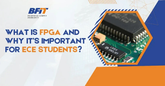
As an Electronics & Communication Engineering (ECE) student, you must have heard the term FPGA a couple of times. But what exactly is it? Why is everyone talking about it? And most importantly, what does it do for you in your professional life? Well, let’s break it down in the easiest possible manner.
In the modern tech world, electronics is no longer about wires & resistors. The field has expanded & it now encompasses advanced systems such as embedded processors, IoT devices & digital logic designs. And that is where FPGA for ECE students comes in as a lifesaver. Studying FPGA can provide you with a solid advantage, particularly if you intend to work in electronics, robotics, chip design or embedded systems.
What is FPGA in Electronic Engineering?
FPGA is short for Field-Programmable Gate Array. In simple terms, it’s a digital chip that can be programmed after manufacturing. Unlike standard processors (such as the one in your PC), which have pre-programmed functions, FPGAs can be reprogrammed to do many different things.
The good thing about FPGA is that you can create your own logic circuits on it such as creating a tiny processor or creating a custom system tailored to your requirements. This is what makes FPGAs so great in the world of electronics so when someone asks what is FPGA in electronic engineering, they’re referring to a device that allows engineers to create digital systems from the ground up, all in a single chip.
Why Is FPGA Important for ECE Students?
Being an ECE student, you’re supposed to understand how electronic systems operate — not only theoretically but practically as well. This is where FPGA for ECE students comes into the picture. With FPGA, you don’t merely study logic gates or flip-flops; you build systems that use them.
This hands-on experience teaches you about digital design in depth. You get to see how signals travel, how timing occurs & how circuits actually function in the real world. This is something that textbooks can’t teach yet it’s exactly what employers are seeking when they hire.
Other than this, here’s why FPGA is important for ECE students:
• Boosts Practical Knowledge & Skills
FPGAs are commonly used in industries such as telecommunication, defence, medical electronics & consumer equipment. So, becoming familiar with working with FPGA provides practical skills. You will learn about tools such as VHDL or Verilog (for programming FPGA) & simulation tools like Xilinx or Altera.
When you have FPGA for ECE students in your resume, it proves that you not only know theory but can also design & test actual systems. This differentiates you from others at the time of internships, interviews & placements.
• Opens Up Career Opportunities in Core Electronics
One of the big benefits of studying FPGA is that it leads to core electronics career opportunities. Most ECE students end up in IT or software jobs since they don’t have hands-on experience with hardware. But with a good knowledge of FPGA, you can target jobs in embedded systems, VLSI design, robotics, or even the aerospace industry.
Also read: https://bfitgroup.in/fpga-and-its-importance-for-ece-students/
0 notes
Text
Electronic Components Market Challenges: Growth, Share, Value, Size, and Scope
"Executive Summary Electronic Components Market :
Data Bridge Market Research analyzes that the global electronic components market was valued at USD 484,625.45 million in 2023 and is expected to reach USD 700,061.60 million by 2031, registering a CAGR of 8.5% during the forecast period of 2023-2030.
This Electronic Components Market report aids to establish correlative relationship between the product brand and consumers’ needs and preferences. This market research report is a comprehensive analysis on the study of industry. Market research covered in this report helps the management of a firm in planning by providing accurate and up- to-date information about the consumer’s demands, their changing tastes, attitudes, preferences, and buying intentions etc. Further, manufacturer can adjust production according to the conditions of demand which are analysed here. It also supports to secure economies in the distribution of products and find out the best way of approaching the potential. With the data covered in this Electronic Components Market report, marketing of goods can be made efficient and economical which leads to elimination of all type of wastage.
This Electronic Components Market report makes focus on the more important aspects of the market like what the market recent trends are. The market study provides details of drivers and restraints for the Electronic Components Market with the help of SWOT analysis, along with the impact they have on the demand over the forecast period. It provides guidelines about planning of advertising and sales promotion efforts. Furthermore, the Electronic Components Market report helps the manufacturer in finding out the effectiveness of the existing channels of distribution, advertising programmes or media, selling methods and the best way of distributing the goods to the eventual consumers.
Discover the latest trends, growth opportunities, and strategic insights in our comprehensive Electronic Components Market report. Download Full Report: https://www.databridgemarketresearch.com/reports/global-electronic-components-market
Electronic Components Market Overview
**Segments**
- **Component Type**: The electronic components market can be segmented based on component type into passive components, active components, and electromechanical components. Passive components include resistors, capacitors, inductors, and transformers. Active components consist of semiconductor devices like transistors, diodes, and integrated circuits. Electromechanical components incorporate connectors, switches, relays, and sensors. Each segment plays a crucial role in the functioning of electronic devices and systems.
- **End-User Industry**: The market can also be segmented by end-user industry, including automotive, consumer electronics, industrial machinery, healthcare, aerospace and defense, and telecommunications, among others. The demand for electronic components varies across these industries based on factors such as technological advancements, regulatory requirements, and consumer preferences. For instance, the automotive sector requires robust and reliable components for safety and performance, while the consumer electronics sector focuses on miniaturization and power efficiency.
- **Distribution Channel**: In terms of distribution channels, the electronic components market can be segmented into direct sales and distribution sales. Direct sales involve manufacturers selling components directly to end-users or OEMs, while distribution sales involve the use of distributors, wholesalers, and retailers to reach a wider customer base. The choice of distribution channel can impact factors like pricing, product availability, and customer service.
**Market Players**
- **Texas Instruments**: Texas Instruments is a prominent player in the global electronic components market, known for its diverse range of semiconductor products and solutions. The company serves various industries and has a strong reputation for innovation and quality.
- **Murata Manufacturing Co., Ltd.**: Murata Manufacturing Co., Ltd. is a leading Japanese manufacturer of electronic components, specializing in capacitors, inductors, and other passive components. The company has a global presence and is known for its cutting-edge technologies.
- **Infineon Technologies AG**: Infineon Technologies AG is a key player in the active components segment, offering semiconductor solutions for automotive, industrial, and consumer applications. The company's products are known for their performance and reliability.
- **STMicroelectronics**: STMicroelectronics is a multinational semiconductor company that caters to a wide range of end-user industries. The company's product portfolio includes microcontrollers, sensors, and power management solutions.
The global electronic components market is highly competitive and dynamic, with key players constantly innovating to meet evolving customer needs and technological advancements. Demand for electronic components is driven by factors such as the proliferation of IoT devices, the growth of smart manufacturing, and the increasing adoption of electric vehicles. As the market continues to expand, players need to focus on product differentiation, strategic partnerships, and effective distribution channels to maintain a competitive edge.
The global electronic components market is witnessing significant growth propelled by the increasing integration of electronics in various industries such as automotive, consumer electronics, healthcare, and telecommunications. One of the emerging trends in the market is the rising demand for miniaturization and enhanced power efficiency in electronic devices. This trend is driving manufacturers to develop compact and energy-efficient components to meet the evolving needs of consumers and industries. Moreover, the advancement of technologies such as Internet of Things (IoT) is driving the demand for a wide range of electronic components that are essential for the connectivity and functionality of IoT devices.
In addition, the automotive sector is experiencing a surge in demand for electronic components due to the growing trend of electric vehicles and autonomous driving technologies. This shift towards electric vehicles is fueling the demand for advanced components such as power management solutions, sensors, and connectivity devices. The need for reliable and high-performance electronic components in the automotive industry is pushing manufacturers to innovate and develop robust solutions to meet the stringent requirements of this sector.
Furthermore, the aerospace and defense industry is another significant end-user segment driving the growth of the electronic components market. The sector relies heavily on electronic components for mission-critical applications, where precision, reliability, and durability are paramount. As aerospace and defense technologies continue to evolve, the demand for advanced components that can withstand extreme conditions and deliver high performance is expected to rise.
Moreover, the healthcare industry is increasingly incorporating electronic components in medical devices, equipment, and IoT-enabled healthcare systems. Electronic components play a vital role in monitoring, diagnostics, and treatment technologies in the healthcare sector, driving the need for specialized components that meet strict regulatory standards and ensure patient safety.
Overall, the electronic components market is poised for continued growth driven by rapid technological advancements, increased digitization across industries, and the expanding adoption of smart devices and IoT solutions. Market players need to focus on innovation, product diversification, and strategic partnerships to capitalize on the opportunities presented by this dynamic market landscape. By staying ahead of trends and leveraging emerging technologies, electronic component manufacturers can position themselves for growth and success in the competitive global market.The electronic components market is experiencing significant growth driven by the increasing integration of electronics across various industries such as automotive, consumer electronics, healthcare, and telecommunications. One of the key trends shaping the market is the rising demand for miniaturization and enhanced power efficiency in electronic devices. Manufacturers are focusing on developing compact and energy-efficient components to meet the evolving needs of consumers and industries. This trend is further fueled by the advancement of technologies like the Internet of Things (IoT), which is driving the demand for a wide range of electronic components essential for the connectivity and functionality of IoT devices.
The automotive sector is a major driver of demand for electronic components, particularly with the growing trend towards electric vehicles and autonomous driving technologies. The shift towards electric vehicles is creating a need for advanced components such as power management solutions, sensors, and connectivity devices. Manufacturers are under pressure to innovate and develop robust solutions to meet the stringent requirements of the automotive industry for reliable, high-performance electronic components.
Another significant end-user segment propelling the growth of the electronic components market is the aerospace and defense industry. This sector heavily relies on electronic components for mission-critical applications where precision, reliability, and durability are paramount. As aerospace and defense technologies continue to evolve, the demand for advanced components capable of withstanding extreme conditions and delivering high performance is expected to increase.
Moreover, the healthcare industry is progressively incorporating electronic components in medical devices, equipment, and IoT-enabled healthcare systems. These components play a crucial role in monitoring, diagnostics, and treatment technologies in the healthcare sector, driving the need for specialized components that meet stringent regulatory standards and ensure patient safety.
Overall, the electronic components market is poised for continuous growth fueled by rapid technological advancements, increased digitization across industries, and the expanding adoption of smart devices and IoT solutions. Market players need to prioritize innovation, product diversification, and strategic partnerships to leverage the opportunities presented by this dynamic market landscape. By staying abreast of trends, embracing emerging technologies, and focusing on quality and reliability, electronic component manufacturers can position themselves for growth and success in the fiercely competitive global market.
The Electronic Components Market is highly fragmented, featuring intense competition among both global and regional players striving for market share. To explore how global trends are shaping the future of the top 10 companies in the keyword market.
Learn More Now: https://www.databridgemarketresearch.com/reports/global-electronic-components-market/companies
DBMR Nucleus: Powering Insights, Strategy & Growth
DBMR Nucleus is a dynamic, AI-powered business intelligence platform designed to revolutionize the way organizations access and interpret market data. Developed by Data Bridge Market Research, Nucleus integrates cutting-edge analytics with intuitive dashboards to deliver real-time insights across industries. From tracking market trends and competitive landscapes to uncovering growth opportunities, the platform enables strategic decision-making backed by data-driven evidence. Whether you're a startup or an enterprise, DBMR Nucleus equips you with the tools to stay ahead of the curve and fuel long-term success.
Key Benefits of the Report:
This study presents the analytical depiction of the global Electronic Components Marketindustry along with the current trends and future estimations to determine the imminent investment pockets.
The report presents information related to key drivers, restraints, and opportunities along with detailed analysis of the global Electronic Components Market share.
The current market is quantitatively analyzed from to highlight the Global Electronic Components Market growth scenario.
Porter's five forces analysis illustrates the potency of buyers & suppliers in the market.
The report provides a detailed global Electronic Components Market analysis based on competitive intensity and how the competition will take shape in coming years
Browse More Reports:
Global Fanconi-Bickel Syndrome Market Global Virtual Sensor Market Europe Exoskeleton Market Global Soap Dispenser Market Global Nanorobotics Market Global Nut-Free Milk Alternatives Market North America Electronic Medical Records (EMR) Market Global Swine Specialty Feed Additives Market Global Solar Micro Inverter Market Global Dermatology Drugs Market Global Colour Diagnostic Ultrasound Scanner Market Global Micro and Nano Programmable Logic Control (PLC) Market North America Drug Delivery Market Global Insulated Packaging Market Global Mammography Workstation Market Global Winter Wear Market Global Automatic Carton Erector Market Global Prescription Lens Market Europe Uninterruptible Power Supply (UPS) Market Global Plastic Surgery Instruments Market Global 3D Sensor Market North America Fall Detection System Market Middle East and Africa Vagus Nerve Stimulation Market North America Explosion-Proof Equipment Market Asia-Pacific Cancer Diagnostics Market Global Neuronal Ceroid-Lipofuscinoses Market North America Cosmetic Pigments and Dyes Market
About Data Bridge Market Research:
An absolute way to forecast what the future holds is to comprehend the trend today!
Data Bridge Market Research set forth itself as an unconventional and neoteric market research and consulting firm with an unparalleled level of resilience and integrated approaches. We are determined to unearth the best market opportunities and foster efficient information for your business to thrive in the market. Data Bridge endeavors to provide appropriate solutions to the complex business challenges and initiates an effortless decision-making process. Data Bridge is an aftermath of sheer wisdom and experience which was formulated and framed in the year 2015 in Pune.
Contact Us: Data Bridge Market Research US: +1 614 591 3140 UK: +44 845 154 9652 APAC : +653 1251 975 Email:- [email protected]
0 notes
Text
What Makes STN Negative Blue LCD Display Modules the Ideal Visual Interface?
In the fast-paced world of embedded systems and portable electronics, clarity and reliability in display technology are essential. Among the various display types available today, STN Negative Blue LCD Display Modules stand out due to their crisp visibility, energy efficiency, and suitability for compact designs. With advancements in microcontrollers, sensors, and thermal management systems, integrating efficient display modules has become more crucial than ever. This blog explores the features, benefits, and applications of STN Negative Blue LCD Modules and how they align with the demands of modern electronic designs.
Understanding STN Negative Blue Technology
A brief look at what STN Negative Blue LCD means
STN (Super Twisted Nematic) Negative Blue LCD Modules are monochrome displays that utilize a twisted nematic field structure to create sharp contrasts. These modules display white or light-colored characters against a dark blue background, offering excellent readability in various lighting environments.
Compared to traditional TN displays, STN modules provide better viewing angles and contrast, making them suitable for instrumentation, industrial electronics, and mobile devices. Their negative mode enhances the visual quality in dark surroundings, which is ideal for controllers and embedded microprocessor-based systems.
Key Features of STN Negative Blue LCD Modules
What sets these modules apart from others?
These display modules are known for their distinctive blue backgrounds and low power requirements. Their integration into electronics and hardware applications offers several valuable attributes:
Excellent contrast for character-based display interfaces
Wide viewing angles for operator convenience
Compatibility with various microcontrollers and interface types
Low current consumption suitable for battery-powered devices
Rugged performance under thermal and electrical stress
Because they don’t rely on backlight-intensive designs like OLEDs, they work efficiently in devices such as handheld tools, laptops, or portable measurement instruments with capacitors and fuses installed for stable performance.

Advantages That Matter in Real-World Applications
Why engineers and designers prefer STN Negative Blue LCDs
In practical terms, these modules provide a perfect balance of visibility and energy savings. Especially in devices like:
Environmental sensors
Thermal controllers
Programmable switches
Contactors in safety systems
Industrial-grade microprocessor applications
Furthermore, their long operational life and temperature tolerance make them a viable solution for use in both indoor and outdoor electronic enclosures, like those utilizing thermal pads or oils for heat regulation.
Integration With Modern Electronics Ecosystems
How they seamlessly support today’s hardware demands
STN Negative Blue LCD Modules can be easily integrated with various system components, such as:
Cables and connectors for streamlined assembly
Microcontrollers and microprocessors that drive visual data
Capacitors and resistors to ensure voltage stability
LEDs and backlight control circuits
External switches and buttons for user interaction
Embedded tools and grips for user operation in compact spaces
The ease of integration enhances their appeal for embedded designs, including those with real-time monitoring and control functionalities.
Applications Across Industries
Versatile deployment across various sectors
Due to their readability and reliability, STN Negative Blue LCD Display Modules find use in multiple sectors:
Medical Equipment – Displaying sensor data and diagnostic outputs
Industrial Controllers – Integrating with automation systems using contactors and cables
Portable Instruments – Handheld multimeters, insulation testers, or signal analyzers
Consumer Electronics – From smart home thermostats to digital timers and microcontroller-based appliances
Automotive Systems – For speed, temperature, or warning indicators using LEDs and thermal fuses
They are also frequently found in embedded laptop components and robust field-use test tools due to their performance in extreme environments.
Choosing the Right STN Negative Blue LCD Module
Tips for selecting a module based on your project needs
Before integrating a display module, consider the following parameters to ensure you select the best fit:
Size and resolution – Ensure compatibility with your system layout
Interface compatibility – Such as parallel or serial communication
Operating temperature range – Crucial for thermal-critical applications
Mounting options – Depending on your enclosure and internal hardware like grips or tools
Brightness and backlight control – Especially if your design includes LEDs or dimmers
Consulting datasheets and considering safety margins for voltage and current ��� through the use of proper capacitors and fuses — also helps optimize overall product performance.
STN Negative Blue vs. Other LCD Types
A clear edge in various conditions
While TN LCDs offer fast refresh rates and OLEDs deliver vibrant visuals, STN Negative Blue LCDs maintain a strong foothold due to:
Better visibility in low-light or no-backlight applications
Lower cost and power draw compared to OLED modules
Better data readability for character-based interfaces
Enhanced longevity for systems with microcontrollers and electronics accessories
These characteristics make them more practical for devices that value durability, simplicity, and energy efficiency.
Final Thoughts: The Future of STN Negative Blue Displays
Bridging traditional interfaces with next-gen electronics
As the electronics industry continues to evolve with smarter tools, controllers, and sensors, the demand for reliable display solutions remains high. STN Negative Blue LCD Modules fulfill this requirement through their versatility, performance, and compatibility with today’s sophisticated electronic components like thermal regulators, safety contactors, and high-efficiency microprocessors.
Incorporating these modules into your product design not only ensures robust performance but also keeps your devices lightweight, readable, and efficient — hallmarks of modern engineering.
0 notes
Text
Powering the Future: Integrated Voltage Regulator Market to See Robust Growth Through 2031

The global Integrated Voltage Regulator (IVR) market was valued at US$ 5.6 billion in 2023 and is projected to expand at a compound annual growth rate (CAGR) of 6.6% between 2024 and 2031, reaching US$ 9.3 billion by the end of the forecast period. Integrated voltage regulators are critical power-management components that ensure stable and efficient voltage supply in modern electronic systems, from smartphones to electric vehicles.
Market Overview
Integrated Voltage Regulators (IVRs) combine semiconductor voltage regulation and pass components into a single integrated circuit (IC), reducing external components, improving efficiency, and minimizing PCB footprint. By streamlining power-management designs, IVRs replace complex PMIC solutions often dependent on discrete capacitors, resistors, and inductors offering manufacturers cost-effective, space-saving solutions for consumer electronics, automotive systems, industrial equipment, and more.
IVRs maintain constant output voltage amidst fluctuating input, supporting optimal device operation. Common applications range from laptop adapters and desktop motherboards to onboard automotive electronics and industrial automation controllers. As miniaturization accelerates and energy-efficiency requirements tighten, the adoption of IVRs is set to surge across multiple sectors.
Market Drivers & Trends
Miniaturization of Consumer Electronics: The consumer electronics market’s relentless push for thinner, lighter devices is driving demand for compact power-management ICs. IVRs, with minimal external components, enable portable electronics—smartphones, tablets, wearables—to shed bulk and reduce board complexity.
Automotive Electronics Proliferation: Electric and hybrid vehicles, advanced driver-assistance systems (ADAS), and infotainment platforms require stable, high-efficiency voltage regulation solutions. IVRs optimize battery management, reduce heat dissipation, and ensure consistent power delivery to critical safety and performance systems.
Power Efficiency and Thermal Management: Lower power consumption and improved thermal profiles are imperative for battery-powered devices. IVRs deliver high conversion efficiency, minimizing wasted energy and extending battery life in IoT endpoints, medical wearables, and handheld industrial instruments.
Industry 4.0 and IoT Expansion: The rise of smart factories and connected devices elevates the need for reliable power-supply modules. IVRs support distributed power architectures, providing precise voltage regulation across sensor networks, actuators, and edge-computing nodes.
Latest Market Trends
Hybrid Converter Designs: Manufacturers are blending inductive switching and switched-capacitor techniques to strike a balance between efficiency and size. Hybrid architectures leverage the low EMI of capacitive regulators and high efficiency of inductive designs for optimized performance.
Digital Control and Programmability: Digitally adjustable on-the-fly voltage scaling and fault-protection features are becoming standard. Programmable IVRs allow system designers to tailor voltage rails dynamically, improving transient response and system reliability.
Embedded Inductor Integration: Advanced packaging techniques now embed inductors directly within the IC substrate. Such Fully Integrated Voltage Regulators (FIVRs) reduce external BOM and improve power density, as demonstrated by recent 3D-stacked chiplet architectures.
Automotive-Grade Qualification: Stringent AEC-Q100 certification requirements are pushing IVR vendors to deliver parts qualified for extreme temperature, vibration, and reliability needs of automotive applications.
Key Players and Industry Leaders
The global IVR market is moderately consolidated, with leading semiconductor firms and specialized power-IC vendors competing on efficiency, integration level, and feature set. Prominent players profiled in the latest market report include:
Analog Devices, Inc.
Empower Semiconductor, Inc.
Globaltech Semiconductor Co., Ltd.
Infineon Technologies AG
Intel Corporation
Microchip Technology Inc.
Nisshinbo Micro Devices Inc.
NXP Semiconductors N.V.
Qualcomm Incorporated
Renesas Electronics Corporation
Semtech Corporation
STMicroelectronics N.V.
Texas Instruments Incorporated
Vishay Intertechnology, Inc.
Other Key Players
Recent Developments
January 2023: Nisshinbo Micro Devices launched the NR1600 series LDO regulators, supporting up to 500 mA output and 6.5 V input rating for consumer and industrial applications.
March 2022: Empower Semiconductor introduced the EP71xx quad-output step-down IVR series, offering up to 12 A per channel with digitally controlled dynamic voltage scaling, eliminating the need for external passives.
June 2022: Intel unveiled its FIVR architecture featuring embedded inductors and self-trimmed, digitally controlled ON-Time DCM approaches, achieving up to 37.6% higher efficiency than traditional LDOs in 22 nm 3D-TSV stacked packages.
March 2020: ABLIC Inc. released the S-19310/S-19315/S-19316 automotive LDO regulator series with integrated voltage monitoring, targeting safety-critical in-vehicle systems.
Market Segmentation
By Component: LDO, Inductive Switching (buck-boost), Switched-Capacitor, Hybrid, Pure.
By Input Voltage: Low (<7 V), Mid (7–30 V), High (>30 V).
By Packaging: 2.5D, Flip Chip, WLCSP, 3D IC, FOWLP, Hybrid Bonding, SiP, Others.
By Application: Automotive (Infotainment, ADAS, Battery Management), Consumer Electronics (Wearables, Computing, Home Appliances), Energy & Utility (Energy Meters, Solar), Industrial (HMI, HVAC, Motor Drives), IT & Telecom (Base Stations, Data Centers), Aerospace & Defense, Others (Healthcare, Oil & Gas).
By Geography: North America, Europe, Asia Pacific, Central & South America, Middle East & Africa.
Access key findings and insights from our Report in this sample - https://www.transparencymarketresearch.com/sample/sample.php?flag=S&rep_id=86198
Regional Insights
Asia Pacific (APAC): Dominant market with 42.2% share in 2023, driven by China’s consumer electronics manufacturing, expanding IoT deployment in Southeast Asia, and robust industrial automation investment in South Korea and Japan.
North America: Strong foothold with rapid adoption in automotive electronics and edge data-center power supplies. The U.S. market benefits from Intel, Texas Instruments, and Analog Devices’ R&D hubs.
Europe: Growth fueled by stringent energy-efficiency regulations and electrification of transport. Germany and France lead in automotive and industrial power-management uptake.
Central & South America, MEA: Emerging opportunities in telecom infrastructure, renewable-energy inverters, and mining automation projects.
Market Opportunities
Electric Vehicle (EV) Expansion: As EV penetration accelerates globally, the need for high-efficiency, automotive-grade IVRs for battery management and auxiliary systems grows exponentially.
5G Infrastructure Rollout: Telecom base stations and small cells require multi-rail power supplies with fast transient response—an apt use case for digitally controlled IVRs.
Wearable and Medical Electronics: Regulatory approval and miniaturization demands create niches for ultra-small, low-noise LDO and buck-boost IVRs in health-monitoring devices.
Renewable Energy Systems: Distributed solar inverters and microgrid controllers benefit from compact, high-current IVRs that can manage variable DC inputs from photovoltaic panels.
Future Outlook
The integrated voltage regulator market is poised for sustained growth through 2031, underpinned by continuing device miniaturization, rising automotive electrification, and the digital transformation of industrial systems. Continued R&D into new materials, monolithic magnetic integration, and AI-driven control algorithms will further boost regulator efficiency and functionality, unlocking fresh applications across emerging sectors.
Why Buy This Report?
Comprehensive Data: In-depth analysis of historical data (2017–2022) and forward-looking forecasts to 2031.
Strategic Insights: Detailed chapter on Porter’s Five Forces, value-chain mapping, and regulatory environment.
Competitive Intelligence: Profiles of 15+ key players, including market share analysis and strategic roadmaps.
Segmentation Analysis: Cross-segment and regional breakdowns highlight high-growth pockets.
Actionable Recommendations: Expert perspectives on technology trends, investment hotspots, and risk mitigation strategies.
Flexible Formats: Delivered in PDF and fully editable Excel formats for custom data querying.
Explore Latest Research Reports by Transparency Market Research: Photonic Integrated Circuits (PIC) Market: https://www.transparencymarketresearch.com/photonic-integrated-circuit.html
Non-volatile Memory Express (NVMe) Market: https://www.transparencymarketresearch.com/non-volatile-memory-express-nvme-market.html
E-Beam Wafer Inspection System Market: https://www.transparencymarketresearch.com/e-beam-wafer-inspection-system-market.html
Filtered Connectors Market: https://www.transparencymarketresearch.com/filtered-connectors-market.html
About Transparency Market Research Transparency Market Research, a global market research company registered at Wilmington, Delaware, United States, provides custom research and consulting services. Our exclusive blend of quantitative forecasting and trends analysis provides forward-looking insights for thousands of decision makers. Our experienced team of Analysts, Researchers, and Consultants use proprietary data sources and various tools & techniques to gather and analyses information. Our data repository is continuously updated and revised by a team of research experts, so that it always reflects the latest trends and information. With a broad research and analysis capability, Transparency Market Research employs rigorous primary and secondary research techniques in developing distinctive data sets and research material for business reports. Contact: Transparency Market Research Inc. CORPORATE HEADQUARTER DOWNTOWN, 1000 N. West Street, Suite 1200, Wilmington, Delaware 19801 USA Tel: +1-518-618-1030 USA - Canada Toll Free: 866-552-3453 Website: https://www.transparencymarketresearch.com Email: [email protected]
0 notes
Text
Linear Winding Machines: Features, Types & Applications
Winding machines are in high demand due to their integral role in manufacturing essential electronic components such as resistors, capacitors, and inductors. These components are crucial for building any electronic circuit, with inductors specifically relying on winding machines for their production. Inductors, also known as coils, are fundamental components in electronics. Learn about linear winding machines, their role in coil manufacturing, and key features like spindle rotation, traverse control, and programmable functions.
0 notes
Text
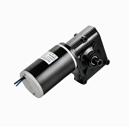
Exploring How the Speed of China DC Brushed Motor Can Be Effectively Controlled
The China DC Brushed Motor remains a widely used electromechanical component in various industries due to its cost-effectiveness, simplicity, and reliability. From small household appliances to industrial machines, these motors offer a straightforward solution for motion control. A critical aspect of their functionality lies in speed regulation. Whether for precision devices or variable-speed tools, controlling motor speed efficiently is essential. This article delves into the common methods used to manage the speed of a China DC Brushed Motor and how each technique impacts performance.
Voltage Control Method
One of the basic and direct ways to adjust the speed of a DC brushed motor is by varying the applied voltage. Since motor speed is nearly proportional to the supply voltage, increasing the voltage results in a higher rotational speed, while decreasing it slows the motor down. This method is simple and effective, especially in low-cost systems. However, it offers limited precision and may affect torque output and efficiency at lower voltages. Additionally, voltage drops under load can cause speed instability, making this approach less suitable for applications requiring consistent performance.
Pulse Width Modulation (PWM)
PWM is the commonly used method for precise speed control in a China DC Brushed Motor. Instead of reducing voltage directly, this technique turns the power on and off rapidly using electronic switches. By adjusting the duty cycle—the proportion of time the power is "on" during each cycle—PWM effectively controls the average voltage supplied to the motor. This allows for highly efficient speed modulation without significant power loss or heat generation. PWM also enables smoother acceleration and deceleration and is widely supported by microcontrollers and motor drivers, making it ideal for modern automation systems.
Closed-Loop Feedback Control
For applications where stable and accurate speed is critical, closed-loop systems are used. These systems integrate sensors, such as encoders or tachometers, that continuously monitor the motor’s speed and provide real-time feedback to a controller. The controller compares the actual speed to the desired value and adjusts the input (often via PWM) accordingly. This setup compensates for load changes or supply fluctuations and ensures consistent performance. Though more complex and costly, closed-loop control offers high precision and is frequently employed in robotics, CNC machines, and other demanding environments using China DC Brushed Motors.
Resistive Speed Control (Less Common Today)
In the past, series resistors were often used to drop voltage and thereby reduce motor speed. While still occasionally seen in low-tech or educational applications, this method is inefficient, as the resistor dissipates energy as heat. It also causes voltage instability under load and provides poor control resolution. As such, resistive methods are now largely obsolete compared to PWM and electronic controllers.
Digital Motor Controllers
Modern digital controllers bring together advanced techniques for controlling China DC Brushed Motors. These systems often combine PWM modulation, feedback loops, and interface options for programmable speed settings. Some even support communication protocols like CAN, UART, or I²C, allowing for integration into larger embedded systems. These controllers not only enhance speed control accuracy but also improve safety, protection, and diagnostics.
Conclusion
Controlling the speed of a China DC Brushed Motor involves a range of techniques, from simple voltage adjustments to advanced PWM and closed-loop systems. Each method has its strengths and trade-offs, with the choice depending on application requirements such as cost, precision, and energy efficiency. As technology evolves, smarter and more integrated control systems continue to expand the versatility of these reliable motors, ensuring their relevance across both traditional and modern industries.
Performance Highlights: Output Speed and Torque: The motor offers a versatile range of speed and torque options, allowing for customization to suit specific application requirements. The gearbox provides precise control over speed and torque output. Efficiency: With its brushed DC technology and precision gearbox, this motor delivers high efficiency, minimizing energy consumption and heat generation. Reliability: The 7712Z motor is designed for continuous operation with minimal wear and tear, ensuring a reliable performance over an extended lifespan.
0 notes
Text
Why Do Electronic Devices Rely on Voltage Regulators? Discover Their Role in Reliable Power Management
In the complex world of electronics, maintaining consistent and precise voltage levels is essential for stable operation. Voltage regulators are the components tasked with this responsibility. They safeguard electronic circuits from power fluctuations, ensuring each part of a system functions correctly and efficiently. Whether in smartphones, medical devices, or industrial machines, voltage regulators form the foundation of dependable power delivery.
Modern devices are more compact and power-sensitive than ever. To accommodate these needs, Power Management ICs (PMICs) integrate voltage regulators into a single chip, streamlining energy distribution across various modules while optimizing board space and reducing heat.
What Makes Voltage Regulators Indispensable in Modern Technology?
Voltage regulators manage energy flow within an electronic circuit by keeping the output voltage at a steady level, regardless of variations in input voltage or current draw. This stability prevents component damage, data corruption, and overheating.
Two main approaches are used to regulate voltage:
Linear Regulation – In this method, excess input voltage is dissipated as heat. It’s simple, low-noise, and ideal for analog applications but less efficient.
Switching Regulation – This technique involves rapidly switching elements on and off to control energy transfer. It uses inductors and capacitors to maintain output voltage and offers high efficiency, especially for battery-powered systems.
Each approach suits different power requirements, with linear regulators preferred for simplicity and switching regulators chosen for efficiency.
What Are the Primary Types of Voltage Regulators?
Different electronic systems demand different power control techniques. To meet these demands, several types of voltage regulators have been developed:
Fixed Voltage Regulators Deliver a specific, constant output voltage. Commonly used in basic electronic projects and legacy systems.
Adjustable Voltage Regulators Provide a user-defined output voltage through external resistors, allowing more control for complex circuit needs.
Low Dropout (LDO) Regulators Efficient in low-voltage scenarios, these require only a minimal difference between input and output voltages and are favored in portable devices.
Buck (Step-Down) Converters Reduce input voltage to a lower output voltage with high efficiency, ideal for powering low-voltage microcontrollers from higher-voltage sources.
Boost (Step-Up) Converters Increase input voltage to a higher output voltage. Common in systems where a small power source, like a battery, must supply higher-voltage components.
Buck-Boost Converters Adaptively raise or lower voltage based on input conditions, offering flexibility for unstable power sources.
How Do Power Management ICs Improve Efficiency with Built-In Regulators?
Power Management ICs are comprehensive solutions that include multiple voltage regulators in a compact chip. These integrated circuits optimize how power is distributed across processors, memory, communication modules, and sensors.
Reduce the need for multiple discrete regulators on a board
Minimize power loss and heat generation
Simplify circuit design and reduce footprint
Allow programmable voltage settings for dynamic power demands
PMICs are widely used in mobile devices, embedded systems, and IoT applications where power efficiency and miniaturization are priorities.
Where Are Voltage Regulators Used Across Industries?
Voltage regulators are not confined to just one sector. Their versatility makes them a backbone in numerous applications:
Automotive Electronics Stabilize voltage for sensors, infotainment systems, LED lighting, and engine control units under constantly changing electrical conditions.
Consumer Electronics Ensure consistent power delivery to cameras, smartphones, gaming consoles, and laptops, improving battery performance and device lifespan.
Medical Equipment Deliver safe and steady power to critical instruments like heart monitors, diagnostic devices, and portable defibrillators.
Industrial Automation Manage power for programmable logic controllers (PLCs), motors, and robotic systems operating in high-demand, noisy environments.
Telecommunication Infrastructure Provide efficient power to signal processors, antennas, and routers, supporting high-speed data transmission.
What Should You Consider When Choosing a Voltage Regulator?
Selecting the right voltage regulator requires evaluating several technical factors that align with your application’s needs:
Input and Output Voltage Range Ensure compatibility between source and required device voltage.
Current Capacity Choose a regulator that can handle the peak current draw without overheating.
Efficiency Requirements For battery-powered or heat-sensitive designs, prioritize switching regulators or PMICs with high efficiency.
Noise Sensitivity For audio, RF, or precision analog systems, opt for linear regulators with minimal ripple and electromagnetic interference.
Thermal Management Consider regulators with built-in thermal protection or those requiring heat sinks for high-load operations.
Why Are Voltage Regulators Critical for Next-Generation Electronics?
As electronic systems continue to grow more powerful and compact, the importance of voltage regulation increases. Designers must strike a balance between performance, efficiency, and size. Voltage regulators, particularly those integrated into Power Management ICs, enable engineers to meet these demands by delivering reliable, adaptable, and energy-efficient power solutions.
Their role goes beyond simply powering circuits — they form the nerve center of power distribution, enabling innovation across industries.
1 note
·
View note
Text
Revolutionizing Monofilament Yarn Manufacturing: Trends and Innovations
Technology continues to shape and enhance every aspect of industrial manufacturing, and monofilament yarn manufacturers are embracing cutting-edge advancements to improve efficiency, sustainability, and accuracy. Modern monofilament yarn-making machines are now capable of producing high-quality yarns used in diverse applications, including ropes, nets, brushes, and fishing lines.
Among the most commonly used yarn types are PET monofilament yarns (polyethylene terephthalate) and PP monofilament yarns (polypropylene). Known for their strength, durability, and versatility, these materials are essential across various industries. With increasing technological progress, monofilament yarn extrusion machines are evolving to meet the growing demands of monofilament yarn manufacturers, ensuring optimal production and superior product quality.
Here are the top trends shaping the future of monofilament yarn production.

Energy-Efficient Monofilament Yarn-Making Machines
Energy efficiency is now a key priority in yarn manufacturing, with industry leaders adopting eco-friendly solutions to minimize energy consumption and reduce costs.
A groundbreaking innovation in sustainable production is the introduction of energy-regenerative units, which replace traditional braking resistors. These systems capture excess heat generated by machinery and convert it into usable power, optimizing energy usage and cutting down on waste.
This transformation highlights a major step toward greener manufacturing, helping businesses reduce carbon footprints while maintaining high output quality.
Enhancing Efficiency and Accuracy
With increased global demand, efficiency and precision in yarn production have become critical. Manufacturers are now integrating PLC (Programmable Logic Controller) central control systems, which significantly improve operational accuracy.
These advanced control systems offer:
Remote monitoring and automation – allowing manufacturers to track machine performance in real-time.
Improved production yields – optimizing resource usage and minimizing material waste.
Seamless integration with office computers and HMI systems – enabling 24/7 factory surveillance, even with limited manpower.
This technology has streamlined machinery installation, troubleshooting, and training, enhancing productivity while ensuring high-precision production.
Customized Yarn-Making Solutions
To better serve diverse market needs, manufacturers are shifting toward customized, flexible solutions in monofilament yarn production.
By adopting tailored approaches, manufacturers can:
Improve efficiency, optimizing operations and reducing lead times.
Enhance product quality, ensuring yarns meet specific industry standards.
Adapt to evolving customer demands, remaining competitive in the global market.
This trend toward personalized manufacturing allows monofilament yarn manufacturers to boost productivity while maintaining high-quality output.
Embracing Industry 4.0 Technologies
The future of monofilament yarn production is centered around Industry 4.0 innovations, including:
IoT-enabled automation
Production processing management
Real-time data storage & analysis
Automated machine control
These advancements allow manufacturers to monitor production conditions in real time, ensuring greater precision, lower waste, and optimized performance. By leveraging data-driven insights, businesses can achieve better efficiency and scalability in monofilament yarn extrusion.
Must-Have Features in Next-Generation Yarn-Making Machines
As demand for high-quality monofilament yarn continues to grow, manufacturers must ensure their machinery includes advanced features for efficient, seamless production.
Modern yarn-making machines should incorporate:
Energy-saving technology – optimizing electricity usage and reducing operating costs.
Enhanced data storage & analysis – providing insights into production efficiency and material handling.
Automated control systems – streamlining production and minimizing manual intervention.
Real-time monitoring capabilities – ensuring precision in output and troubleshooting.
Additionally, ensuring compatibility with multiple materials—including recycled PP, HDPE, PA, PET materials, and PET flakes—is crucial for sustainable, eco-friendly production.
Conclusion: Advancing Monofilament Yarn Production
The monofilament yarn extrusion industry is rapidly evolving, embracing automation, customization, and sustainability to enhance manufacturing efficiency. With the integration of smart machinery, energy-efficient solutions, and data-driven innovations, monofilament yarn manufacturers are paving the way for higher-quality, cost-effective production.
Investing in cutting-edge monofilament yarn-making machines ensures manufacturers stay competitive, reducing costs while optimizing output and product precision.
Are you ready to upgrade your yarn production line? Consider these must-have features when selecting high-performance extrusion machines for maximum efficiency and seamless operation.
0 notes
Text
OBDSTAR DC706 Volvo HCM R/W Data, Coding, Change Left Side
This article will demonstrate how to use OBDSTAR DC706 to read and write data, read coding, and modify left or right-side settings on the Volvo HCM module. It also supports OBDSTAR X300 Classic G3.
Required Tools: DC706 ECU Tool High-power DC regulated power supply Main cable ECU clone jumper 120Ω resistor MP001 Programmer Volvo HCM module
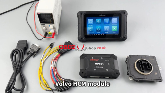
Procedure Before proceeding, you need to upgrade the software to the latest version.
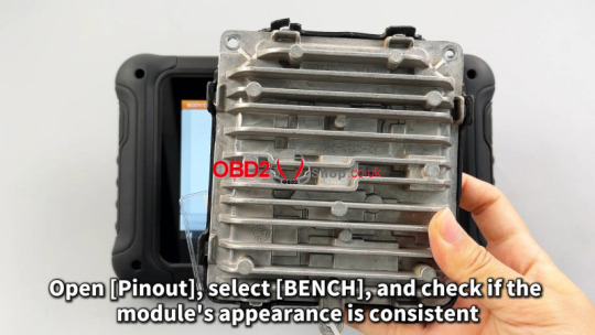
ECU Flasher >> BODY/CHASSIS/OTHER >> Latest version >> VOLVO HCM(OLD) CONTINENTAL RIGHT R7F7010244 >> Pinout >> BENCH, MP001, OK Check if the module's appearance is consistent.
Click "Guide" and carefully read the warm reminder, function description, operation introduction, and connection method. Connect the device according to the wiring diagram.


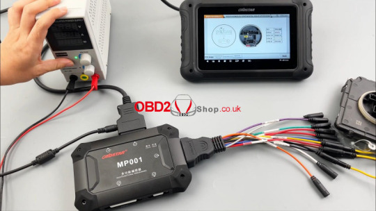
After connecting, click "Start". BENCH >> MP001 >> OK This function is available when connecting to the service. Please ensure the Internet connection is normal. Click "Connect >> OK".
Here, we can read and write coding, read and write INT flash(R7F7010244), and change the left side.
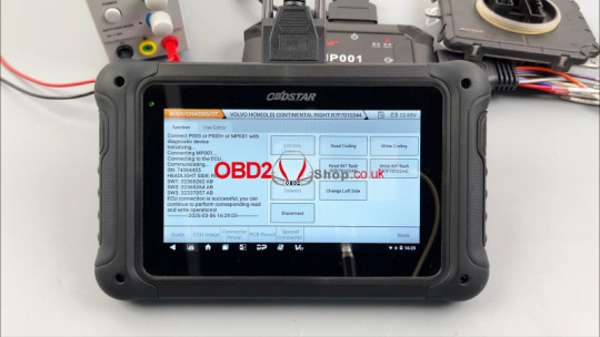


www.obd2shop.co.uk
0 notes
Text
AVR HV UPDI FTW!
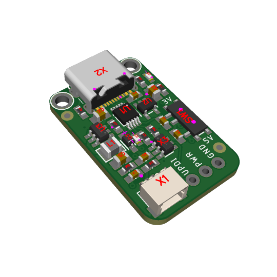
We have been working a lot with attiny816 and attiny1616 chips (https://www.adafruit.com/search?q=attiny) lately, as for our seesaw boards. We often must program them with a CP2102-based breakout (https://www.adafruit.com/product/5335) with a 4.7K resistor soldered between the RX and TX pins. But we are longing for a nicer programmer. Perhaps one that can select 3V or 5V power and logic? And activity LED? and 12V High Voltage programming support if we accidentally set the HV-Only fuse? We looked around and found this charming open-source hardware design (https://github.com/wagiminator/AVR-Programmer/tree/master/SerialUPDI_HV_Programmer), and it inspired us to make something similar.
Instead of a USB A plug, going with USB C. We've used the CH9102F (https://www.adafruit.com/product/5568) but never the CH340E, but it seems like it will do the job here. The classic 3.3V AP2112K LDO is kept for power, and the MT3806 booster looks neat, so that goes on too… plus the 3/5V selection switch! The most significant change is going with a COS4561 analog switch for the 12V/UART signal swapping and a JST SH 3-pin for connecting a quick wire harness (https://www.adafruit.com/product/5755). It fits nicely on a single-sided PCB; most of the space goes to the booster and analog switch, so we'll make a non-HV version.
#attiny816#attiny1616#electronicsDIY#CP2102Breakout#seesawBoards#UPDIProgramming#OpenSourceHardware#USBCTech#SerialProgramming#CircuitDesign
3 notes
·
View notes