#Edge Reflow
Text
JavaScript Frameworks
Step 1) Polyfill
Most JS frameworks started from a need to create polyfills. A Polyfill is a js script that add features to JavaScript that you expect to be standard across all web browsers. Before the modern era; browsers lacked standardization for many different features between HTML/JS/and CSS (and still do a bit if you're on the bleeding edge of the W3 standards)
Polyfill was how you ensured certain functions were available AND worked the same between browsers.
JQuery is an early Polyfill tool with a lot of extra features added that makes JS quicker and easier to type, and is still in use in most every website to date. This is the core standard of frameworks these days, but many are unhappy with it due to performance reasons AND because plain JS has incorporated many features that were once unique to JQuery.
JQuery still edges out, because of the very small amount of typing used to write a JQuery app vs plain JS; which saves on time and bandwidth for small-scale applications.
Many other frameworks even use JQuery as a base library.
Step 2) Encapsulated DOM
Storing data on an element Node starts becoming an issue when you're dealing with multiple elements simultaneously, and need to store data as close as possible to the DOMNode you just grabbed from your HTML, and probably don't want to have to search for it again.
Encapsulation allows you to store your data in an object right next to your element so they're not so far apart.
HTML added the "data-attributes" feature, but that's more of "loading off the hard drive instead of the Memory" situation, where it's convenient, but slow if you need to do it multiple times.
Encapsulation also allows for promise style coding, and functional coding. I forgot the exact terminology used,but it's where your scripting is designed around calling many different functions back-to-back instead of manipulating variables and doing loops manually.
Step 3) Optimization
Many frameworks do a lot of heavy lifting when it comes to caching frequently used DOM calls, among other data tools, DOM traversal, and provides standardization for commonly used programming patterns so that you don't have to learn a new one Everytime you join a new project. (you will still have to learn a new one if you join a new project.)
These optimizations are to reduce reflowing/redrawing the page, and to reduce the plain JS calls that are performance reductive. A lot of these optimatizations done, however, I would suspect should just be built into the core JS engine.
(Yes I know it's vanilla JS, I don't know why plain is synonymous with Vanilla, but it feels weird to use vanilla instead of plain.)
Step 4) Custom Element and component development
This was a tool to put XML tags or custom HTML tags on Page that used specific rules to create controls that weren't inherent to the HTML standard. It also helped linked multiple input and other data components together so that the data is centrally located and easy to send from page to page or page to server.
Step 5) Back-end development
This actually started with frameworks like PHP, ASP, JSP, and eventually resulted in Node.JS. these were ways to dynamically generate a webpage on the server in order to host it to the user. (I have not seen a truly dynamic webpage to this day, however, and I suspect a lot of the optimization work is actually being lost simply by programmers being over reliant on frameworks doing the work for them. I have made this mistake. That's how I know.)
The backend then becomes disjointed from front-end development because of the multitude of different languages, hence Node.JS. which creates a way to do server-side scripting in the same JavaScript that front-end developers were more familiar with.
React.JS and Angular 2.0 are more of back end frameworks used to generate dynamic web-page without relying on the User environment to perform secure transactions.
Step 6) use "Framework" as a catch-all while meaning none of these;
Polyfill isn't really needed as much anymore unless your target demographic is an impoverished nation using hack-ware and windows 95 PCs. (And even then, they could possible install Linux which can use modern lightweight browsers...)
Encapsulation is still needed, as well as libraries that perform commonly used calculations and tasks, I would argue that libraries aren't going anywhere. I would also argue that some frameworks are just bloat ware.
One Framework I was researching ( I won't name names here) was simply a remapping of commands from a Canvas Context to an encapsulated element, and nothing more. There was literally more comments than code. And by more comments, I mean several pages of documentation per 3 lines of code.
Custom Components go hand in hand with encapsulation, but I suspect that there's a bit more than is necessary with these pieces of frameworks, especially on the front end. Tho... If it saves a lot of repetition, who am I to complain?
Back-end development is where things get hairy, everything communicates through HTTP and on the front end the AJAX interface. On the back end? There's two ways data is given, either through a non-html returning web call, *or* through functions that do a lot of heavy lifting for you already.
Which obfuscates how the data is used.
But I haven't really found a bad use of either method. But again; I suspect many things about performance impacts that I can't prove. Specifically because the tools in use are already widely accepted and used.
But since I'm a lightweight reductionist when it comes to coding. (Except when I'm not because use-cases exist) I can't help but think most every framework work, both front-end and Back-end suffers from a lot of bloat.
And that bloat makes it hard to select which framework would be the match for the project you're working on. And because of that; you could find yourself at the tail end of a development cycle realizing; You're going to have to maintain this as is, in the exact wrong solution that does not fit the scope of the project in anyway.
Well. That's what junior developers are for anyway...
2 notes
·
View notes
Text
Sony Unveils New NW-A306 Walkman

Sony has introduced a new music player, the NW-A306 to the Walkman series family. The NW-A306 is designed for users looking for high-quality sound and style. Weighing just 113 grams, equipped with WiFi connectivity, a 3.6” touch screen and tactile physical music controls, it's designed to be used on the go whilst being immersed in a high-quality music experience.
The premium aluminium milled frame on the NW-A306 provides superior rigidity for low impedance and precise, stable sound and solid bass.
NW-A306 main features
S-Master HX digital amp technology, independently developed for Walkman is compatible with the native DSD format. It reduces distortion and noise across a wide range of frequencies, for rich and full-bodied sound, further enhanced by new high-quality sound lead-free solder.
Just like the latest Signature Walkman model, the NW-A306 applies a reflow solder containing gold, whose effect is significant in the overall improved sound localisation and wider sound space. To realise the music player’s evolutionary sound, a dual clock, film capacitor and fine sound register have been precisely placed within the Walkman.
The NW-A306 uses Edge-AI (Artificial Intelligence), and DSEE Ultimate (Digital Sound Enhancement Engine) which accurately upscales compressed digital music files to higher quality. The evolving algorithm now delivers even greater benefits for CD-quality (16-bit 44.1/48kHz) lossless codec audio. Restoring acoustic subtleties and dynamic range provides a richer, more complete listening experience.
With further progress from its predecessor models, listeners can enjoy DSEE Ultimate for upscaling music, whether it is Wi-Fi streamed or downloaded. Plus DSEE Ultimate can also be enjoyed with wireless headphones.
The NW-A306 features a longer battery life than previous models so listeners can immerse themselves in more of their music. The NW-A306 has a battery life of up to 36 hours of 44.1kHz Flac playback, up to 32 hours of 96kHz FLAC high-resolution audio playback or up to 26 hours with the streaming service app to meet user demand.
Sustainability in mind
Sony products are not only designed to be stylish but also with the environment in mind. No plastic is used in the packaging material for the NW-A306, reflecting Sony’s commitment to reducing the environmental impact of our products and practices.
Pricing and availability
NW-A306 will retail price for £350 / €400 and will be available to purchase across Europe from January 2023.
Read the full article
2 notes
·
View notes
Text
Optimized SMT Circuit Board and PCB Assembly Manufacturing: A Guide to Modern Electronics Production
In the ever-evolving world of hardware, the SMT (Surface Mount Technology) circuit board and PCB (Printed Circuit Board) assembly fabricating forms have gotten to be progressively vital. These advances not as it were empower the creation of smooth, compact, and high-performance electronic gadgets but moreover play an imperative part in the victory of different businesses, from shopper hardware to aviation and beyond.
Understanding the SMT Circuit Board Manufacturing Process
The SMT circuit board fabricating prepare includes the situation and fastening of electronic components specifically onto the surface of a printed circuit board. This approach offers a few focal points over conventional through-hole innovation, including:
1. Miniaturization: SMT components are by and large littler and more compact than their through-hole partners, permitting for the creation of littler and more lightweight electronic devices.
2. Increased Productivity: The robotized pick-and-place machines utilized in SMT fabricating can collect components on a circuit board much quicker than manual patching, moving forward generation efficiency.
3. Enhanced Unwavering quality: The patch joints in SMT gatherings are regularly more dependable and less inclined to disappointment than those in through-hole designs.
4. Cost Investment funds: SMT fabricating frequently decreases the in general fetched of electronic components and congregations, making them more open to a more extensive run of businesses and consumers.
The PCB Assembly Manufacturing Process
The PCB Assembly Manufacturing includes the integration of different electronic components onto a printed circuit board to make a useful electronic gadget. This prepare ordinarily incorporates the taking after steps:
1. PCB Manufacture: The to begin with step is the generation of the printed circuit board itself, which includes the creation of copper follows, cushions, and other highlights on a non-conductive substrate, such as fiberglass or ceramic.
2. Component Situation: Once the PCB is manufactured, electronic components, such as resistors, capacitors, coordinates circuits, and connectors, are put onto the board utilizing computerized pick-and-place machines or manual assembly methods.
3. Soldering: After the components are set, they are fastened onto the PCB utilizing procedures like wave patching, reflow patching, or specific fastening, depending on the particular necessities of the assembly.
4. Inspection and Testing: The amassed PCB is at that point assessed and tried to guarantee that all components are legitimately associated, and the circuit is working as intended.
5. Finishing Forms: Depending on the application, the PCB may experience extra wrapping up forms, such as conformal coating, embodiment, or the expansion of warm sinks or shielding.
The Significance of SMT Circuit Board andPCB Assembly Manufacturing
The SMT Circuit Board and PCB assemblyfabricating forms are basic for the generation of a wide run of electronic gadgets, from shopper hardware to mechanical hardware and past. These advances empower the creation of compact, lightweight, and profoundly solid electronic components and congregations, which are basic for assembly the ever-increasing request for progressed, feature-rich electronic devices.

Furthermore, the SMT circuit board and PCB gathering fabricating forms play a pivotal part in the competitiveness of different businesses, as they permit for the quick and cost-effective generation of electronic items. This, in turn, leads to progressed time-to-market, diminished fabricating costs, and upgraded item quality, all of which are basic for keeping up a competitive edge in today's worldwide marketplace.
Conclusion
The SMT circuit board and PCB assemblyfabricating forms are at the heart of the advanced gadgets industry, empowering the creation of imaginative and mechanically progressed items that proceed to change our world. By understanding the complexities and benefits of these forms, producers and originators can use these advances to make items that are not as it were outwardly engaging and profoundly useful but too cost-effective and dependable.
0 notes
Text
Understanding Special PCB: The Backbone of Customized Electronics
In today’s rapidly evolving technology landscape, Special PCBs (Printed Circuit Boards) have become a cornerstone in customized electronics, playing a pivotal role in industries like aerospace, healthcare, telecommunications, and automotive. These specialized boards are tailored to meet unique design requirements and performance standards that exceed conventional PCB capabilities.

What are Special PCBs?
Special PCBs are distinct from standard circuit boards due to their specific materials, layout designs, and intended applications. These boards are used for devices that operate in harsh environments, require higher performance, or need to be compact and efficient. Whether it’s rigid-flex PCBs, aluminum-based PCBs for LED lighting, or multilayer boards, special PCBs are designed to cater to niche market needs.
The Role of PCB Manufacturing in Special PCBs
Creating special PCBs demands cutting-edge PCB manufacturing processes and advanced technology. The production of these PCBs involves multiple stages, including:
Design and Prototyping: Advanced software is used to design the layout, followed by the creation of prototypes for testing.
Material Selection: Special materials, such as ceramic, polyimide, or copper-clad laminates, are chosen based on the application’s specific needs.
Precision Assembly: The manufacturing of special PCBs requires high-precision assembly techniques like surface mount technology (SMT) and through-hole assembly to ensure reliability and performance.
PCB Board Makers: Experts in Customization
Leading PCB board makers like Shenzhen Shuoqiang Electronics (SQPCB) specialize in delivering high-quality special PCBs tailored to individual specifications. With state-of-the-art manufacturing facilities, SQPCB can handle small-scale prototype projects or large-scale production orders, ensuring precision, durability, and performance.
Assembly of Special PCBs
PCB manufacturing assembly is a critical phase where components are mounted onto the PCB substrate. For special PCBs, the assembly process requires meticulous attention to detail due to their complexity. Whether it’s high-density interconnect (HDI) boards or PCBs with intricate multilayer designs, the right assembly process ensures the optimal functionality of the circuit.
The PCB assembly process typically involves:
Soldering Components: High-quality soldering methods, like reflow soldering, are used to attach components to the board accurately.
Testing and Quality Control: After assembly, PCBs undergo rigorous testing to ensure they meet quality standards and perform as intended in their specific applications.
Why Choose SQPCB for Special PCB Manufacturing?
SQPCB stands out as a trusted PCB board maker for several reasons:
Customization: Their team of experts works closely with clients to deliver customized special PCBs tailored to specific requirements.
Advanced Technology: They use the latest tools and technologies to ensure the highest standards of manufacturing and assembly.
Quality Assurance: With a robust quality control process, every PCB manufactured by SQPCB is rigorously tested to ensure reliability and performance.
Competitive Pricing: SQPCB offers cost-effective solutions without compromising on quality, making them a preferred partner for businesses of all sizes.
Conclusion
Special PCBs are critical in driving innovation in various sectors, offering unmatched performance and adaptability for custom electronic devices. By partnering with experienced PCB board makers like SQPCB for PCB manufacturing and assembly, businesses can ensure the production of high-quality, reliable, and efficient special PCBs for their unique applications.
#Special PCB#pcb manufacturing#customize pcb#flex pcb#pcb manufacturers#multilayer pcb#advertising#rigid flex pcb#business
0 notes
Text
The Essentials of PCB Assembly: A Comprehensive Guide
Printed Circuit Boards (PCBs) are the backbone of modern electronic devices. They connect and support various electronic components, facilitating the flow of electrical currents and signals. PCB assembly is the process of integrating these components onto the board to create a functional electronic device. This blog will explore the intricacies of PCB assembly, its stages, and its significance in the electronics industry.
Understanding PCB Assembly
PCB assembly (PCBA) is a multi-step process that involves mounting electronic components onto a PCB. The assembly process can be broadly divided into two categories: Surface Mount Technology (SMT) and Through-Hole Technology (THT). SMT involves placing components directly onto the surface of the PCB, while THT requires inserting component leads through holes in the PCB and soldering them in place.
Key Stages of PCB Assembly
Solder Paste Application: The process begins with applying solder paste to the PCB. This is typically done using a stencil to ensure that the paste is applied only to the areas where components will be placed. The solder paste consists of tiny solder balls suspended in flux, which helps the solder adhere to the board.
Component Placement: Once the solder paste is applied, the next step is to place the electronic components onto the PCB. In modern manufacturing, this is often done using automated machines known as pick-and-place machines. These machines accurately place components onto the board based on the design files.
Reflow Soldering: After the components are placed, the board is passed through a reflow oven. The oven heats the solder paste, causing it to melt and form solid solder joints, which securely attach the components to the PCB. Once the board exits the oven, the solder cools and solidifies, forming a strong mechanical and electrical bond.
Inspection and Quality Control: Quality control is crucial in PCB assembly to ensure the reliability and functionality of the finished product. Inspections can be performed manually or using automated optical inspection (AOI) systems. These systems check for various defects, such as solder bridging, missing components, and misalignments.
Through-Hole Component Insertion: For boards that require through-hole components, the insertion process can be manual or automated. The leads of the components are inserted through the holes and soldered in place, usually using wave soldering or selective soldering techniques.
Functional Testing: After assembly, the PCB undergoes functional testing to verify that it operates as intended. This testing can include electrical tests, in-circuit tests (ICT), and functional tests. Any issues detected during testing are addressed and corrected.
The Importance of PCB Assembly
PCB assembly is a critical phase in the electronics manufacturing process. The quality and precision of the assembly directly impact the performance and reliability of the final product. Here are some reasons why PCB assembly is essential:
Miniaturization: Modern electronic devices are becoming increasingly compact. PCB assembly techniques, especially SMT, enable the placement of small, densely packed components, allowing for the miniaturization of electronic devices.
Cost-Effectiveness: Automated PCB assembly reduces labor costs and increases production speed. High-volume manufacturing benefits from economies of scale, making electronic products more affordable for consumers.
Reliability: Proper PCB assembly ensures robust connections and reduces the risk of component failure. High-quality assembly processes result in reliable and durable electronic devices.
Innovation: Advancements in PCB assembly technology drive innovation in the electronics industry. New assembly methods and materials contribute to the development of cutting-edge electronic products.
Conclusion
PCB assembly is a complex but essential process that brings electronic designs to life. From solder paste application to functional testing, each step requires precision and expertise. The ongoing advancements in assembly technology continue to push the boundaries of what is possible, enabling the creation of smaller, faster, and more reliable electronic devices. As the electronics industry evolves, the importance of PCB assembly will only continue to grow, shaping the future of technology.
By understanding the intricacies of PCB assembly, engineers, manufacturers, and enthusiasts can appreciate the effort and skill involved in producing the electronic devices we rely on every day. For more details visit our website www.crimpcircuits.com

#pcb manufacturing toronto#printed circuit board design#metal clad pcb#printed circuits#rigid flex pcb#full turnkey pcb services#turnkey pcb services#pcb parts#eagle software#pcb designing#flexible pcb#pcb assembly#printed circuit board manufacturers#pcb manufacturers in canada#circuit board manufacturers in canada#pcb quote#pcb prototype services in canada
0 notes
Text
Industrial Oven Manufacturers in Chennai | High-Quality Ovens
We manufacture variety of high quality industrial ovens like curing, drying, baking, reflow, batch,conveyor and clean room ovens that come with cutting edge technology. We export gas-fired exchangers to various countries and the demand for our products are increasing steadily.
Industrial ovens manufacturers in tamilnadu will comes out from our state-of-the-art manufacturing facility comes with fully automated control systems. Manufacturing, engineering and production industries can curtail their overheads to a great extent when they start using our branded industrial ovens that comes with plenty of automated functionalities.
We will install the industrial ovens inside your factories according to the rules framed by government authorities. Team of engineers and technicians will erect, test run and commission the industrial oven. They will work according to your directions and satisfy your requirements.
The industrial oven that we manufacture and supply comes with guarantee and warranty. It will withstand day-today stress, strains and wear and tear. Foremen can operate our industrial ovens round- the-clock hassle-free. It is worth noting that the industrial ovens that comes out from our factories are ISO certified products.
#industrialOvenManufacturersInTamilNadu#industrialOvenManufacturersInChennai#industrialOvenManufacturersInHosur#industrialOvenInTamilNadu#industrialOvenInKerala#industrialOvenInAndhra#industrialOvenInTelangana#industrialOvenInKarnataka#industrialOvenManufacturersInBangalore#industrialOvenManufacturersInMumbai#industrialOvenExporters#industrialOvenExportersInIndia#industrialOvenManufacturersInIndia
0 notes
Text
Leading the Way: PCB Assembly Excellence in California's Thriving Tech Hub
In the heart of California's bustling tech hub, PCB Assembly stands as a cornerstone of innovation, efficiency, and precision engineering. This comprehensive guide explores the significance of PCB Assembly in California, highlighting key processes, industry trends, benefits, and the pivotal role it plays in driving technological advancements across diverse sectors.
The Significance of PCB Assembly in California
California's tech landscape is renowned for its vibrant ecosystem of startups, established companies, research institutions, and tech enthusiasts. At the core of this ecosystem lies PCB Assembly, a critical process in electronics manufacturing that involves assembling and soldering electronic components onto printed circuit boards (PCBs). PCBs serve as the central nervous system of electronic devices, enabling the interconnection and functionality of components such as microprocessors, memory modules, sensors, and connectors.
Key Processes in PCB Assembly
PCB Design and Layout: The PCB Assembly process begins with meticulous design and layout using CAD (Computer-Aided Design) software. Design engineers in California leverage their expertise to create PCB layouts that optimize signal integrity, minimize electrical noise, and ensure efficient component placement.
Component Procurement: Once the PCB design is finalized, components such as resistors, capacitors, integrated circuits (ICs), and connectors are sourced from trusted suppliers. California's tech industry benefits from a robust supply chain network, ensuring access to high-quality components for PCB Assembly.
Surface Mount Technology (SMT) Assembly: SMT Assembly is a key aspect of PCB manufacturing, where electronic components are mounted directly onto the PCB's surface using solder paste and reflow soldering processes. This method offers high precision, density, and reliability in component placement.
Through-Hole Assembly: In addition to SMT, Through-Hole Assembly involves inserting components with wire leads through pre-drilled holes on the PCB and soldering them on the opposite side. This process is used for components that require additional mechanical support or higher power handling capabilities.
Inspection and Testing: Quality assurance is paramount in PCB Assembly. California-based manufacturers employ advanced inspection techniques such as Automated Optical Inspection (AOI), X-ray inspection, and functional testing to detect defects, ensure solder joint integrity, and validate PCB functionality.
Industry Trends and Innovations
California's PCB Assembly industry is at the forefront of technological advancements and industry trends:
Miniaturization and High-Density Interconnects: The demand for smaller, lightweight electronic devices drives innovations in miniaturization techniques and high-density interconnects (HDI), enabling complex PCB designs with reduced form factors and increased functionality.
Advanced Materials and Substrates: PCB Assembly in California incorporates advanced materials such as flexible substrates, rigid-flex PCBs, and high-frequency laminates to meet the requirements of cutting-edge applications in aerospace, telecommunications, healthcare, and IoT (Internet of Things).
Industry 4.0 Integration: California's PCB Assembly facilities embrace Industry 4.0 technologies such as robotics, AI (Artificial Intelligence), IoT-enabled manufacturing systems, and data analytics for real-time monitoring, predictive maintenance, and process optimization.
Green Manufacturing Practices: Sustainability is a priority in California's tech industry. PCB Assembly facilities adopt eco-friendly practices, recycling initiatives, lead-free soldering processes, and energy-efficient manufacturing techniques to minimize environmental impact.
Benefits of PCB Assembly in California
Innovation Ecosystem: California's PCB Assembly sector thrives within a rich ecosystem of innovation, collaboration, and knowledge exchange, fostering breakthroughs in technology, product design, and market competitiveness.
Skilled Workforce: The state's tech-savvy workforce comprises skilled engineers, technicians, and manufacturing specialists adept at PCB design, assembly, testing, and quality assurance, ensuring industry-leading standards and reliability.
Access to R&D Resources: California offers access to world-class research and development (R&D) resources, universities, and technology incubators, enabling continuous innovation, product differentiation, and intellectual property advancement in PCB Assembly.
Proximity to Markets: Being strategically located in California provides PCB Assembly facilities with proximity to key markets, customers, and industry partners, facilitating faster response times, supply chain efficiency, and market insights.
Regulatory Compliance: PCB Assembly in California adheres to stringent regulatory standards such as RoHS (Restriction of Hazardous Substances) and IPC (Association Connecting Electronics Industries) guidelines, ensuring product safety, environmental sustainability, and market acceptance.
Future Outlook and Conclusion
Looking ahead, PCB Assembly in California is poised for continued growth, fueled by advancements in technology, evolving market demands, and a culture of innovation. From IoT devices and autonomous vehicles to 5G telecommunications and renewable energy systems, PCB Assembly will continue to be a driving force behind transformative technologies that shape the future of industries and improve people's lives globally.
In conclusion, PCB Assembly in California epitomizes excellence, innovation, and collaboration in the tech sector. With its robust capabilities, skilled workforce, and commitment to sustainability, California's PCB Assembly industry remains a pivotal player in advancing electronics manufacturing, driving technological progress, and fueling economic growth in the digital age.
0 notes
Text
MacBook Air A1932 13" Retina Liquid Damage Service
Chronicles of Resilience MacBook Air A1932's Battle Against Liquid Threats:~~
The chronicles of resilience unfold as the MacBook Air A1932 13" Retina faces liquid threats head-on. Whether it's an accidental spill, a sudden downpour, or an unforeseen mishap, the device engages in a battle where every component plays a crucial role.
The first line of defense is often the sealed enclosure, designed to shield the internal components from liquid intrusion. As liquid attempts to breach this fortress, the MacBook Air A1932 activates its intricate mechanisms, strategically diverting and resisting the encroaching threat.Choose MacBook Air A1932 13" Liquid Damage Repair for a device that stands resilient in the face of liquid challenges, ready to conquer new horizons.
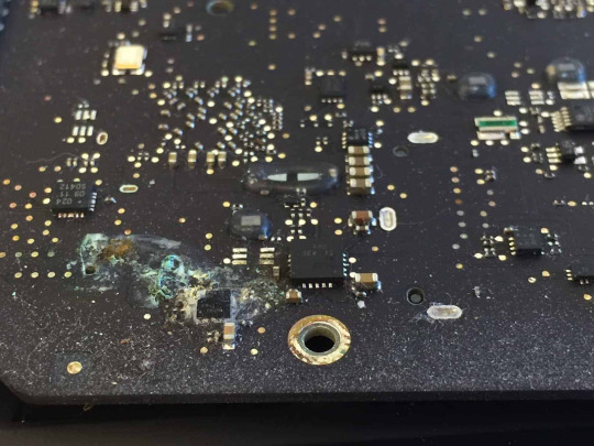
Warning Signs that Liquid May Have Breached Your MacBook Air A1932:~~
Unresponsive Keyboard: If your MacBook Air A1932's keyboard is acting erratic, with keys sticking or not responding, it could be a sign of liquid damage
Trackpad Issues: Liquid damage may cause the trackpad to become unresponsive or exhibit erratic behavior, making precise navigation challenging.
Flickering Screen: A display that flickers or shows distorted visuals might indicate liquid intrusion affecting the internal components.
Strange Noises: Unusual sounds emanating from your MacBook Air A1932, such as hissing or crackling, could be a result of liquid affecting internal components.
Overheating: Liquid damage may compromise the cooling system, leading to overheating issues as the MacBook struggles to regulate temperature.
Battery Draining Quickly: If the battery life suddenly diminishes, it could be a sign of liquid damage affecting the MacBook's power-related components.
System Crashes or Freezing: Frequent system crashes or instances of the MacBook freezing unexpectedly may be indicative of underlying liquid damage.
Unusual Smells: A distinct odor, especially if it's an unusual or burnt smell, could suggest components within your MacBook Air A1932 are affected by liquid damage.
Inconsistent Performance: General performance issues, such as slow response times, application lag, or overall sluggishness, may be linked to liquid damage.
Distorted Audio Output: Liquid damage can impact the MacBook's audio components, leading to distorted or muffled sound during audio playback.
Port Malfunctions: USB ports, Thunderbolt ports, or other connectors may malfunction or fail to recognize connected devices due to liquid exposure.
Visible Liquid Traces: If you notice any visible traces of liquid around the edges of the MacBook or on the keyboard, it's a clear indicator of a potential spill or exposure.
How Our Expert Handling of MacBook Air A1932 Liquid Damage:~~
Immediate Assessment:
Swiftly assessing the extent of liquid damage is crucial. Our technicians promptly evaluate the affected areas, including internal components, to gauge the severity of the situation.
Disassembly and Inspection:
Careful disassembly of the MacBook Air A1932 allows for a thorough inspection of individual components. We meticulously examine the logic board, keyboard, trackpad, connectors, and other critical elements for signs of corrosion or damage.
Advanced Diagnostics:
Our state-of-the-art diagnostic tools aid in pinpointing specific issues caused by liquid exposure. This step ensures a precise understanding of the damage, enabling us to formulate a targeted and effective repair strategy.
Corrosion Mitigation:
Corrosion is a common consequence of liquid damage. Our experts employ advanced techniques to mitigate corrosion, preventing further deterioration of vital components and restoring conductivity.
Component Repair and Replacement:
Damaged components undergo meticulous repair or replacement to ensure the MacBook Air A1932 returns to optimal functionality. This may involve soldering, reflowing, or replacing affected parts with high-quality components.
Thorough Cleaning:
A thorough cleaning process removes any residue left by liquids, preventing long-term damage and ensuring a clean and safe internal environment for your MacBook Air A1932.
Precision Reassembly:
After repairs, each component is meticulously reassembled with precision and attention to detail. Our technicians adhere to industry standards, ensuring the MacBook Air A1932 is restored to its original state.
Functional Testing:
Rigorous functional testing is conducted to ensure that all repaired components work seamlessly together. This step involves checking the keyboard, trackpad, display, ports, and other functionalities to guarantee a comprehensive repair.
Quality Assurance:
Our commitment to quality extends beyond the repair process. Each MacBook Air A1932 undergoes stringent quality assurance checks to ensure that it meets our high standards before being returned to the customer.
Educational Guidance:
As part of our service, we provide guidance on best practices to prevent future liquid damage. This includes tips on handling spills, using protective accessories, and maintaining a liquid-free environment for your MacBook Air A1932.
1 note
·
View note
Text
Exploring the Reflow Oven Machine at Trident Technologies
In the realm of precision engineering and advanced technology, Trident Technologies has continually raised the bar with its cutting-edge solutions. reflow oven machine Among its impressive lineup of innovations, the reflow oven machine stands as a beacon of efficiency and accuracy in electronic manufacturing.At the heart of modern electronics assembly lies the reflow soldering process, a crucial step that demands finesse and precision. Trident's epitomizes this art form, orchestrating the delicate dance of heat, time, and control with remarkable expertise.

What sets Trident's reflow oven apart is its seamless integration of state-of-the-art technology. Equipped with advanced temperature profiling and zone control features, this machine ensures optimal soldering conditions for components, from the smallest microchips to complex circuit boards. https://www.tridentet.com/reflow-oven advantages of Trident's reflow oven machine extend far beyond its technical capabilities. With reduced energy consumption and enhanced productivity, manufacturers experience higher throughput without compromising on quality. This translates to cost-efficiency and consistent, high-quality outputs.
As technology continues to evolve, Trident Technologies remains at the forefront of innovation, constantly refining and enhancing its reflow oven machine to meet the evolving demands of the industry. With a keen eye on sustainability and performance, they pave the way for a more efficient and greener future in electronics manufacturing.In the intricate world of electronics manufacturing, the reflow oven machine stands as a testament to reflow oven machine Trident Technologies' commitment to excellence. Its precision, efficiency, and adaptability make it an indispensable tool in the arsenal of manufacturers worldwide, solidifying Trident's position as a leader in cutting-edge solutions.Trident Technologies' reflow oven machine isn't just a piece of equipment; it's a game-changer in the realm of electronic manufacturing. know more
0 notes
Text
The Recipe for Success: Custom Ovens Tailored to Your Needs

In the world of industrial processes, research, and manufacturing, having the right tools for the job is essential. When standard ovens don't quite fit the bill, custom ovens step in to provide tailored solutions. In this blog, we'll explore the concept of custom ovens, their versatility, and how Savage-Engineered Equipment excels in delivering customized thermal solutions to meet specific industry needs.
Understanding Custom Ovens
Custom ovens, as the name suggests, are ovens that are designed and built to meet unique and specialized requirements. They offer a level of flexibility that standard ovens cannot, making them indispensable in various industries. Whether it's accommodating unconventional shapes, specific temperature and humidity control, or unique size constraints, custom ovens provide the perfect solution.
The Versatility of Custom Ovens
Custom ovens are a versatile tool with applications across a wide range of industries. Here are some key areas where custom ovens shine:
Industrial Manufacturing: Manufacturers often require custom ovens for curing, annealing, and heat treatment processes tailored to their specific materials and product configurations.
Research and Development: Research labs frequently need custom ovens for conducting experiments and tests that demand precise environmental control.
Aerospace and Defense: The aerospace and defense industries rely on custom ovens for heat-treating critical components and materials with strict quality and safety standards.
Electronics: In the electronics sector, custom ovens are vital for reflow soldering, drying, and curing processes that require unique temperature profiles and precision control.
Pharmaceuticals: The pharmaceutical industry utilizes custom ovens for applications such as sterilization, drying, and granulation, where compliance with regulatory standards is paramount.
Savage-Engineered Equipment's Expertise in Custom Ovens
Savage-Engineered Equipment has established itself as a leader in providing custom oven solutions for various industries. With over five decades of experience, their expertise in engineering and manufacturing sets them apart.
Here's why Savage-Engineered Equipment is your ideal partner for custom ovens:
Tailored Solutions: They work closely with clients to understand their specific needs and challenges, resulting in a customized oven that precisely meets their requirements.
Cutting-Edge Technology: Savage-Engineered Equipment leverages the latest technologies in control systems, insulation, and heating elements to ensure optimal performance and energy efficiency.
Quality Assurance: Their custom ovens are designed and manufactured to adhere to rigorous industry standards, ensuring reliability, safety, and consistent results.
Cost-Efficiency: Custom doesn't mean expensive. Savage-Engineered Equipment designs ovens that are cost-effective and energy-efficient, helping businesses reduce operational costs.
Conclusion
Custom ovens are the answer when standard solutions fall short of meeting the specific demands of various industries. With Savage-Engineered Equipment's dedication to delivering tailor-made thermal solutions, businesses can enhance their processes, improve product quality, and meet regulatory requirements.
As industries continue to evolve, the need for custom ovens will persist, and the expertise of companies like Savage-Engineered Equipment will remain essential. For more information on their custom oven solutions, please visit Savage-Engineered Equipment's website at https://savage-engineered.com/ or contact them at 570-329-6500.
0 notes
Text
"Supercharge Your Web Development with React JS: A Step-by-Step Tutorial"
"Supercharge Your Web Development with React JS: A Step-by-Step Tutorial"
The open-source JavaScript package React.js, sometimes known as React, is used to create user interfaces (UIs) for web applications. It was created by Facebook, and Facebook, along with a community of independent developers and businesses, is now maintaining it. React is a popular alternative for developing contemporary web apps because of its component-based architecture and effective method of handling UI modifications.

Let's explore React.js in greater depth:
1.Component-based architecture, for example:
• The component-based architecture used by React divides the user interface into manageable, reusable components. These elements can stand in for many different elements of a web page, including buttons, forms, or full sections.
• Each component contains its own rendering, state, and logic. By allowing developers to concentrate, this modularity streamlines development and maintenance.
2. The usage of a virtual DOM (document object model) is one of React's key advances. React uses a virtual representation of the DOM (the web page's structure) in memory as opposed to directly modifying the actual DOM.
• React efficiently determines the difference (diffing) between the old and new virtual DOM trees when the state of a component changes.
• React updates the DOM only when it is necessary, reducing browser reflows and enhancing performance.
Third, JSX (JavaScript XML):
• Developers may write HTML-like code inside JavaScript files thanks to React's use of the JSX syntax extension. The structure and look of components can be easily defined using JSX.
• By using programs like Babel, JSX code is converted into ordinary JavaScript.
Declarative Syntax: React promotes this type of programming. React controls the rendering, while developers specify how the user interface (UI) should appear based on the current state.
• By using this method, less imperative code is required to directly alter the DOM, making the UI code more predictable and readable.
5. State Administration:
React offers a way to control how components' states are managed. State is a representation of dynamic data, such as dropdown menu visibility or form input values.
• React ensures that the user interface (UI) always represents the current application state by automatically re-rendering the affected components when the state changes.
6. Data Flow in One Direction:
• Data only goes in one direction, often from parent components to child components, thanks to React's enforcement of a unidirectional data flow. This keeps the application's data flow consistent and logical.
Reactive Ecosystem:
• React offers a robust ecosystem with a wide range of libraries and tools, such as:
• React Router: Used for single-page applications' routing and navigation.
• Redux: A well-liked library for centralized and predictable application state management.
• Styled-components and Emotion: Libraries for applying CSS-in-JS styling to React components
• React Native: This is a framework for creating native mobile applications based on React.
8. Large Developer Community and Resources: Since React has a sizable and vibrant developer community, there are a ton of resources, tutorials, and third-party libraries accessible to help with development.
In conclusion, React.js is a strong JavaScript toolkit for creating cutting-edge, engaging, and effective user interfaces in online applications. Developers aiming to construct dynamic and maintainable UIs frequently choose it because of its component-based architecture, virtual DOM, and declarative syntax. React's sizable community and ecosystem ensure that it will develop and continue to be a crucial tool in web development.

I strongly advise getting in touch with ACTE Institution because they provide certifications and opportunities for job placement if you want to learn more about Reacte Js. You can study more effectively with the aid of knowledgeable tutors. These services are available both offline and online. Take things slow, and if you're interested, think about signing up for a course.
1 note
·
View note
Text
Printed Circuit Board Assembly (PCB Board Assembly): The Heart of Modern Electronics
Printed Circuit Board Assembly (PCBA) is a significant cycle in the assembling of electronic gadgets, where electronic parts are mounted and associated with a printed circuit board (PCB). The majority of electronic devices are built on PCBs, which provide the mechanical support and electrical connections necessary for the device to function. The gathering system changes an uncovered PCB into a completely utilitarian board that can be utilized in many applications, from buyer gadgets to modern hardware.
The PCB Assembly Process There are several steps in the PCB Assembly process, all of which are necessary to guarantee the quality and functionality of the final product:

1. Solder Paste Application: The most important phase in PCB gathering is applying bind glue to the region of the PCB where parts will be put. A stencil is utilized to apply the patch glue precisely to the PCB cushions, which are regions where the part leads will interface.
2. Part Situation: After the bind glue is applied, the electronic parts are put on the PCB. Pick-and-place machines, which are automated machines that can quickly and precisely position thousands of components onto a PCB, are typically used for this. Parts utilized in PCBs incorporate resistors, capacitors, coordinated circuits, and connectors.
3. Soldering: To ensure a strong electrical connection, the components must be soldered after being placed on the PCB. There are two chief restricting techniques used in PCB gathering: reflow restricting and wave welding. Wave soldering is used for through-hole components, whereas reflow soldering is commonly used for SMT components.
4. Inspection and Testing: The assembled PCB is examined for flaws such as solder bridges, misaligned components, and incomplete solder joints following soldering. Robotized Optical Review (AOI) and X-ray assessment are usually utilized for this reason. Additionally, functional testing is carried out to guarantee that the PCB will perform as intended in the final application.
5. Final Assembly and Packaging: The last move toward the PCB gathering process is the last get together and bundling. This might include adding heat sinks, fenced in areas, or connectors, and setting up the board for transportation.
Significance of PCB Assembly
PCBA is basic since it straightforwardly influences the exhibition, dependability, and life span of electronic gadgets. A very much gathered PCB guarantees that the gadget works accurately and can endure the afflictions of its expected use. Failures caused by poor assembly can be costly in terms of customer satisfaction, replacement costs, and repairs.
PCB Board Assembly is made even more difficult by the complexity of contemporary electronics, which are becoming smaller and more functional. To meet the increasing demands for improved performance and miniaturization, cutting-edge assembly methods like multi-layer boards and high-density interconnects (HDI) are now commonly used.
In conclusion, the production of electronic devices relies heavily on the Printed Circuit Board Assembly procedure. PCBs are the foundation of all modern electronics, from smartphones to industrial controllers. Understanding the PCB get together cycle is essential for anybody engaged with gadgets plan and assembling, as it assumes a significant part in guaranteeing the usefulness and dependability of the eventual outcome.
1 note
·
View note
Text
Exploring HBM3e Features: What’s New and Noteworthy

The creation of the world’s fastest HBM3e DRAM has been verified by SK hynix, and samples are now being sent to NVIDIA and other clients for testing purposes.
The HBM3e DRAM from SK Hynix is not only faster, but it also provides higher capacities, improved heat dissipation, and easy compatibility.
It was reported in June that NVIDIA had made a request to SK hynix to sample their next-generation HBM3e DRAM. This request became a reality when NVIDIA introduced its GH200 GPU with enhanced HBM3e DRAM, giving up to 5 TB/s bandwidth per chip. SK hynix was able to fulfill this request.
SK Hynix Inc. has issued the following press release to indicate that it has successfully created HBM3E, the next-generation of the highest-specification DRAM for AI applications that is presently available, and that a customer’s examination of samples is now under way.
On top of its expertise as the industry’s single mass supplier of HBM3, the business claimed that the successful creation of HBM3E, the extended version of HBM3 which offers the world’s finest specifications, comes on top of its experience as the extended version of HBM3. With its expertise as the supplier of the industry’s biggest volume of HBM products and the mass-production readiness level, SK hynix wants to mass-produce HBM3E in the first half of next year and strengthen its unparalleled leadership in the AI memory market. This will be accomplished by using its experience as the supplier of the industry’s largest volume of HBM goods.
The business claims that its most recent product not only satisfies the industry’s most stringent criteria for speed, which is the most important need for artificial intelligence memory devices, but also excels in all other areas, such as capacity, heat dissipation, and user-friendliness.
In terms of processing speed, the HBM3E is capable of handling data at a rate of up to 1.15 terabytes (TB) per second. This is the same as being able to process more than 230 Full-HD movies that are each 5GB in size in a single second.
The cutting-edge technology of the Advanced Mass Reflow Molded Underfill, also known as MR-MUF**, has been integrated onto the most recent version of the product, which has resulted in a 10% increase in the rate at which heat is dissipated. In addition to this, it offers backward compatibility, which makes it possible to implement the most recent product onto systems that have already been designed for HBM3 without having to make any modifications to their structures or designs.
MR-MUF: a process of attaching chips to circuits and filling the space between chips with a liquid material when stacking chips instead of laying a film to improve efficiency and heat dissipation
Backward Compatibility: an ability to allow interoperability between an older and a new system without modification to the design, especially in information technology and computing spaces. A new memory product with backward compatibility allows continued use of the existing CPUs and GPUs without modifications to design
“We have a long history of working with SK hynix on High Bandwidth Memory for leading-edge accelerated computing solutions,” said Ian Buck, Vice President of Hyperscale and HPC Computing at NVIDIA. “We look forward to continuing our collaboration with HBM3E to deliver the next generation of AI computing.”
According to Sungsoo Ryu, who serves as the Head of DRAM Product Planning at SK hynix, the business has enhanced its market leadership via the creation of HBM3E. This was accomplished by further expanding the completeness of the HBM product range, which is in the limelight as a result of the growth of AI technology. “SK hynix will also work toward achieving a rapid turnaround in its business by increasing the supply share of the high-value HBM products,”
0 notes
Text
Using Microsoft Word for Amazon KDP Paperback Cover Template
KDP paperback Cover Templates are an excellent tool for authors to highlight what their books contain. Using Amazon KDP, authors can easily and quickly upload their manuscripts and have them ready for publishing on Amazon.com. Authors can use KDP paperback Cover Templates for publishing their books from Kdpinterior. It's easy, so writers have a lot of say in the end output. KDP has features that make it a desirable alternative for self-publishers, such as the freedom to choose your own pricing, royalty rate, and method of receiving cash directly from Amazon.
Before deciding to self-publish, it might be helpful to have your book reviewed by an editor. A skilled editor may help you eliminate typos, streamline your writing, and enhance your novel's general structure. It's easy to overlook typos and grammar issues, even if you're a good writer. That's why it pays to have an experienced editor on board.
Amazon KDP Paperback Cover Templates for 6x9-Inch Books
How eager are you to self-publish your book using Amazon KDP? To save unnecessary effort spent on book formatting, use this fantastic KDP paperback book in Word. Using Microsoft Word, you may make changes and edits to this paperback. It has dimensions of 6 inches by 9 inches.
Using Microsoft Word for Amazon KDP Paperback Cover Template
This 6 by 9 paperback layout is perfect for self-publishing on Amazon. To get started with this KDP template, you can either start from scratch or copy & paste your existing information. The design and structure of this free Amazon KDP template are both professional and adaptable. Find a way to get your hands on a copy and have a look!
Not just a collection of text boxes, our free Word templates are meticulously designed for desktop writing with a focus on organization and consistency in presentation. We also regularly update our free, modern Word templates to make them more user-friendly and text-reflowable.
What Is the Best Way to Use This Paperback KDP Book?
This free book layout template was made for KDP authors and publishers. The professional layout of your 6x9 booklets is within your reach with the help of this template. There is no limit to the amount of text you can enter into this blank KDP paperback layout. Quickly adapt this cutting-edge Amazon KDP template to your specific requirements with a few simple edits. However, this approach is most successful with works of nonfiction.
Excellent Typefaces for This Free Amazon KDP Template
This KDP template is more than just another boring blank Microsoft Word document because of the high-quality fonts used throughout. Serif fonts "EB Garamond" and "Playfair Display" are used throughout the template. Google provides both of these fonts at no cost for your commercial or personal use.
Use this free KDP paperback template in Microsoft Word to lay out your manuscript before sending it out to print on CreateSpace. The process of printing a paperback book is as simple as outlined above. Follow the link below to get even more of our free, editable book templates for Microsoft Word.
Dimensions of Amazon's KDP Paperback
Imagine you've read this whole article, and you're still confused about KDP cover dimensions, and you just have a surface-level comprehension of the topic. After reading this, you will never again Google anything other than "KDP cover size mistake" or "KDP cover dimensions' trouble." The proposed approach makes determining the KDP cover dimensions a breeze. Compatible with books of any shape or size.
This Is the Initial Phase
You should have complete knowledge of the two components associated with the interior template that define the cover proportions:
The total number of pagesInternal Measurements • Depth and Width
Once we have these two pieces of information, we can go to the Amazon KDP website and get the Cover Template. Take this as an example:
Illustration of an Amazon KDP Interior Template, 6 by 9 I
nches
Let's calculate the proportions for a bleed-free 69 print run of a 120-page children's notebook/sketchbook. As was indicated before, we obtained the cover template for this book from KDP Cover templates. Next, we decide on a trim size of 6x9 and a page count of 120.
What Makes a Good Amazon KDP Paperback Cover?
Publishing success on Amazon depends on quality KDP paperback covers. It is the first thing that would attract people to your work, even before the title or description. The KDP paperback cover for your book makes an enormous difference in whether or not people will continue looking into it. Making an excellent cover for your Amazon KDP book is, thus, well worth the effort.
Adobe Photoshop, a widely used graphics editor, can create a stunning cover for a book. But the problem is that Adobe Photoshop isn't exactly user-friendly, and many people have difficulty learning how to use it. Don't freak out if you fall into this category; I have some good news to share with you today.
Making your own Amazon KDP template doesn't need Adobe Photoshop, after all. There are several other graphic editing applications that can do the same thing. In this piece, I'll show you how to use the online tool Canva to create a fantastic cover for your paperback book.
Canva, the best free image editor, is also very easy to use, especially for novice users. The use of Canva does have one major drawback. Amazon KDP files downloaded as PDFs or PNGs from the Amazon site will not load in this editor without some further work. If you keep reading this piece, however, you'll find out how to quickly get around this issue and create stunning designs in Canva by starting with one of their many premade layouts.
The final thought
With Amazon KDP, publishing your book in paperback format is a breeze. However, you should check that you're doing everything right before you publish your Amazon KDP template. If you want to know how to make the most of your Amazon KDP template, this piece is for you.
#AmazonKDPguide#AmazonKDP#CanvaKDPCover#CoverTemplate#KDPbookcovertemplate#KDPPaperbackCoverTemplate
0 notes
Text
Best PCBA Manufacturing Equipment Services in India
PCB is a Printed Circuit Board. It's a significant electronic part, which is a help for electronic parts and a transporter for electrical associations between electronic parts. As it is created by printing the expected picture on the substrate, it is known as a "printed" circuit board. It's most usually produced utilizing copper-clad epoxy sap/glass material compound.
The PCB is frequently comprised of various layers with 4 and 6 being the most normally utilized, depending on the necessary number of sign layers.
At the point when countless PCBs must be made, odds are parts will not be physically bound manually. This is where proficient gathering houses like Seeed will step in, to assist with manufacturing both the uncovered sheets and collect every one of the parts onto the Printed Circuit Boards, or PCBs.
Best PCBA Manufacturing Equipment Services in India - Syrma SGS
Yet, have you at any point thought about how your makers can stick that monstrous number of small parts onto your PCBs? I have, yet that was until I needed to drive through passages of specialized language online about the apparatus that takes care of business. While there's nothing provocative about PCBA producing, understanding how the cerebrums of all hardware are made most certainly gives pleasure and a feeling of achievement. Heaps of thought go into each phase of the gathering system to convey an entirely working board. Furthermore, with the gadgets getting increasingly progressed, the hardware used to make PCBs are steadily improving and more energizing than at any other time.
Best PCBA Manufacturing Equipment Services in India - Syrma SGS
In PCB gathering, there are 4 primary phases of SMT, or Surface Mount Technology get together utilizing the reflow strategy, which are glue application, mechanized part situation, binding, and review. The essential gear expected for PCB gathering incorporates:
Bind Paste Printing machine
Bind Paste Inspection (SPI) machine
Stick Dispensing machine
Pick-and-Place machine
Reflow Soldering machine
Wave Soldering machine (for through-opening parts)
Programmed Optical Inspection (AOI) machine
In-Circuit Test (ICT) Fixture
Practical Validation Test (FVT) Fixture
Best PCBA Manufacturing Equipment Services in India - Syrma SGS
Bind Paste Printing Machine
The initial phase in PCB gathering is the use of bind glue onto the board. Bind glue is a dim shaded goo produced using a combination of minuscule particles of metal compounds; normally of tin, lead, and silver. Consider it a paste that will keep your finished board intact. Without it, parts wouldn't adhere to your uncovered board.
Patch glue (left), PCB stencil laser-cut openings (right)
Before the glue is applied, a PCB stencil is set over the board. A PCB stencil is a tempered steel sheet that has little laser-cut openings that permit patch glue to be applied exclusively to the region of the board where the parts contacts will ultimately sit on the completed PCB, for example, the SMD cushions.
During the use of patch glue, the PCB stencil and the PCB are gotten into a place in the mechanized glue printer. A wiper then, at that point, applies without lead weld glue on the cushions in exact sums. The machine then hauls a cutting edge across the stencil, to spread and store the glue equitably in the ideal regions. After the stencil is taken out, the patch glue will be precisely where we maintain that it should be (ideally).
Best PCBA Manufacturing Equipment Services in India - Syrma SGS
Weld Paste Inspection (SPI) machine
Various industry studies have brought up that up to 70% of SMD binding issues are followed back to inappropriate or inadequate patch glue printing. Thus, the subsequent stage is to check to assume that the binding glue is printed appropriately onto the board. While utilizing great bind glue printing strategies are in many cases enough for PCBs in low volumes, SPI ought to be thought about while producing higher volumes of PCB to stay away from high modification costs.
0 notes
Last Seen Blogs

nyakleves
Not Your Bbygirl😝

every-word-is-a-poetry-itself
Khaaki Badan

nyahb1
Nyamblr

writerspeace
Life's Good

beautymania-blog2
最新医療を用いた
再生美容術が凄すぎる