#Ceramic Core PCB
Text
BSTCeramicPCB Co., LTD offers ceramic PCB (printed circuit boards) for your company's needs. We also offer Alumina Ceramic, Aluminum Nitride, Ceramic Core PCB, Ceramic Base PCB and much more. Quote & Order your ceramic PCBs online.
0 notes
Text
Enhance Your Electronics with Aluminum PCB Boards
Hitech Circuits Co., Ltd. is a top PCB manufacturer in China, dedicated to providing high-quality products. We offer a variety of metal-based printed circuit boards, including Aluminum PCBs, Copper PCBs, Ceramic PCBs, and Metal Core PCBs, all at great prices. Trust us for your PCB needs. Visit our website today!

0 notes
Text
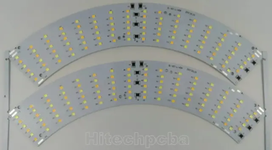
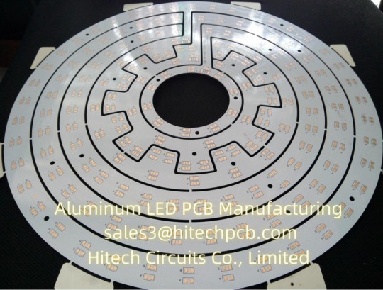
LED PCB Assembly
What is the LED Circuit Board assembly?
Generally, LED PCB assembly is considered to be a circuit board that has the LED components soldered to it. The LED is soldered to the printed circuit board and features a chip that creates the light as electrically connected. A thermal heat sink and a ceramic base are used to bond the chip. Not all the PCB products can be used in Led industry, as an LED PCB is easy to create a high volume of heat, but making it hard to cool with traditional methods. For this reason, metal core PCB is widely used in LED application because of their enhanced ability to dissipate heat, especially aluminum pcb is often used to fabricate PCB for LED lights.
We’ve had great LED PCB assembly experiences with top LED chips to brand such as Cree, Luxeon, Osram, Nichia, Lumileds, MLS, EVERLIGHT, Samsung, LG, Seoul., etc. PCB LED lights can be incorporated into numerous lighting applications due to their combination of excellent energy efficiency, low cost and maximum design flexibility.

Application of LED PCB Assembly
Hitechpcba serves customers in different industries, providing highly reliable and innovative LED PCBs for various applications:
• Horticulture light LED PCB Assembly
• LED controller PCB Assembly
• Computer LED display and indicators
• LED lights PCB Assembly for medical use
• Automotive LED PCBs Assembly include PCBs for brake lights and headlights
• Street lighting LED PCB Assembly
• Flashlights and camping accessories
• Traffic light PCB Assembly
• Commercial lighting LED PCB Assembly
LED PCB Assembly specification
Number of layers for LED PCB
These layers are made up of aluminum and magnesium, but now have Copper base material and Ceramic base materials for LED PCB industry, we can meet it.
Aluminum LED PCBs stand out among other PCBs because it has a good insulation characteristic and has a better machinery performance, the cheap cost is one important factor too.
Types of layers for LED PCB Assembly
Normally, the base layer is made using aluminum alloy metal.
This aluminum alloy substrate used in making the base makes it ideal for through-hole technology which transfers and dissipates heat.
A thermal insulation layer is made using some ceramic polymer which has good viscoelasticity characteristics.
It is highly heat resistant and protects the PCB against heat and mechanical stress.
The circuit layer, which is covered by a copper foil which can range from one to ten ounces.
LED Board type- single or in panel
Some boards are shapeless. For this reason, LED PCB panels are used. This reduces time, labor production and testing time.
Some LED PCB Assembly is done on a single board while others are done on panel boards.
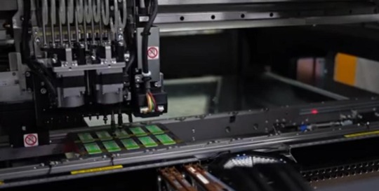
LED PCB Assembly Process
Roughly, the PCBA process can be divided into theses phases: soldering paste printing > SMT (surface mounted technology) > reflow soldering > AOI (automated optical inspection)> THT (through-hole technology) > wave soldering > touch-up and cleaning > IC-programming > FCT (functional tests) > aging testing.
Below we show you the process.
Step1. Summarizing Project Information
Before contacting your supplier, make sure you have all the project information. Suppliers will need info following for quoting LED PCB assembly:
Gerber
BOM
LED PCB specification
Quotation quantity
Once you have gathered these information, you can contact us and request for a quote.
Of course, you can also provide the schematic, LED PCB Assembly pictures and even samples to us. The more details they have, the more accurate the supplier’s quotation will be.
Step2. Discussion and details about custom LED PCB Assembly
Different projects will have different requirements. Remember the special requirements mentioned in step 1? That’s going to be the focus of this session. Equipment and engineering capacity will not be identical between suppliers. Make sure your supplier has the equipment to produce and assemble major components and the corresponding testing capabilities.
For example, some vendors don’t have X-ray testing equipment, which means they can’t check the mount quality of BGA chips. Outsourcing this step will increase risk and cost. That’s what you don’t want.
Also, pay attention to time taken by the supplier to quote. Motherboards often contain hundreds or even thousands of components, and they are supplied by different manufacturers. To ensure the quality of the components, the supplier sourcing team will make multi-inquiries from these manufacturers or authorized suppliers to match customer’s requirement, which usually takes 2-3 business days, and even longer for some scarce chips. Therefore, if your project is complex and the supplier quotes you within few hours, double check with them.
Step3. Sample and feedback
After confirming the PI, the supplier will usually provide pre-production samples for your approval. At the same time, the supplier will also confirm with you the logistics plan of the bulk goods. Make sure they understand your shipping requirements, including details on packaging, customs clearance, taxes, etc.
For us to have a successful LED PCB Assembly process, its functions must be defined. Compliance requirement is defined to reduce the effect when components are selected.
The Bill of Materials is then generated from the information installed on the LED PCB.
All this information is used to assemble components which are identified from MOB to the LED PCB.
After that, the routing of traces is determined to each component, based on the size, shape of the circuit board and location of connectors.

Hitech Circuits is trusted by thousands of electronic engineers on their LED PCB assembly projects, from consumer, led bulb to precisely medical LED light, we can help you from the beginning of design stage; From commercial flood LED to industrial high power LED, from automotive LED to military LED, Venture is the perfect place for your LED PCB assembly requirement.
Hitech Circuits has been participated in hundreds and thousands of LED lighting projects, by providing LED PCB and also LED PCB assembly service.
Our LED PCB assembly had covered both ends of the Lighting Class LED size spectrum, assembling some of the largest (2 meter long boards) and some of the smallest LED Lighting applications which used in Medical Endoscopes.
LED PCB Assembly is very crucial in the current industrial development. Many electrical devises are being innovated and the old once being improved.
LED PCBs are useful due to the fact that they are made using materials that can transfer and dissipate heat. This characteristic increases device durability.
The world is changing with new technology, especially PCB technology that plays an essential role in the application of LED circuits. And the LED industry is taking advantage of this technology and growing faster.
As a full feature PCB solutions provider with more than a decade of experience, we're capable to provide LED PCB fabrication, components procurement and LED PCB assembly all under one roof. We can work with you to develop metal core PCB, aluminum circuit boards customized to your specific applications. We feature competitively priced PCBs made with standard FR-4 material that includes a thermal aluminum clad layer that will efficiently dissipate heat, keep all LED PCB components cool and significantly enhance the performance of your products.

LED pcb board, LED pcb assembly
LED with its advantages of high brightness, high efficiency, low heat, long life, is considered the most development potential in the 21st century lighting. In the market and policy driven by the rapid development of the domestic LED industry blowout has formed a relatively complete industrial chain, including the production of epitaxial wafers, chip preparation, packaging, integration, LED application. In 2010, China's LED industry scale, up from $ 827 billion in 2019 to 220 billion yuan, an annual growth rate of over 70%, higher than the 50% level of growth of the global LED lighting industry output value. Among them, the middle and lower reaches of the most complete industrial chain, accounting for 90% of the overall percentage of the GDP.Chinahas become the world's leading LED manufacturing base and important application market.
To further promote the technological innovation of the LED industry, construction and wide application of independent industry chain, China Electronic Appliance Corporation and industry associations to organize the theme of "Focus on the core energy LED Exhibition will be held November 9-11, 2010 in Shanghai International Expo Center and the 78th China Electronics Fair over the same period will be held will create from raw materials, epitaxial wafers, chip, LED bracket, LED accessories, LED packaging and supporting materials, the LED backlight upstream firm to the upstream and downstream enterprises of the display, lighting, landscaping, decorative lighting, traffic lights, automotive lighting, special lighting, to the equipment, instrumentation, software, finance, consulting and other service enterprises and technological exchanges and market trading platform, help the domestic industry sustained and healthy development, and promote the steady expansion of the LED application market.
In the LED industry chain upstream of the epitaxial wafers and LED chips accounted for 70% of the profits of the whole industry, and technology-intensive, capital-intensive, where the core technology of the LED. Well-known epitaxial wafer and chip production enterprises will be exhibited a number of energy-efficient, low heat, cost-effective LED products, many of whom have excellent products of international advanced level.
LED electronic pcb assembly manufacturing 100% Original LED Chip with one-stop in-house pcba services
3 notes
·
View notes
Text
The Surge of Mandarin PCB Distributors: Exactly How They're Molding the Future of Modern Technology

When you think about sophisticated electronic tools like Apple's apples iphone, you may certainly not promptly connect them along with China's printed circuit board (PCB) distributors. Nevertheless, business like Taiwan's Wistron and China's Shenzhen Kaifa Technology have actually been silently performing an important job in making the complicated PCBs that power these devices. Over the past 3 years, Mandarin PCB providers have actually swiftly expanded their capabilities, and their influence on the international technology field is actually palpable. However what drives their excellence, and how will they form the future of modern technology? The response exists in understanding their exceptional rise.
Past History of Chinese PCB Business
Exactly how did China cheer come to be a prevalent player in the international PCB market? You might be actually startled to find out that China's PCB industry has a past history extending over three decades. In the 1980s, China's federal government launched a collection of financial reforms, leading the technique for international investment and technological move. This triggered the facility of providers like Hitech Circuits Co. Limited, an introducing PCB producer in China. As the business grew, Chinese PCB makers began to focus on creating modern PCB boards, dealing with the demands of worldwide electronics companies. Today, China is home to various PCB board makers, including ceramic PCB manufacturers and light weight aluminum PCB providers. The country's huge production capabilities, coupled along with its reasonable costs and advantageous business setting, have produced it a desirable destination for PCB production.
Benefits of Mandarin PCB Distributors
As China's PCB industry has matured, its own suppliers have actually ended up being considerably attractive to providers seeking reliable, premium PCBs. When trying to find a pcb board distributor, you expect quick delivery, affordable rates, and adherence to quality criteria. Chinese pcb board suppliers have cheered meet these desires, offering a wide array of PCB kinds, including ceramic pcb and aluminum pcb. Their competence in generating complicated PCBs, like double sided pcb supplier, has actually gotten all of them a track record as a best destination for companies requiring high-volume, top notch PCBs. Furthermore, lots of Chinese pcb board distributors have actually invested heavily in trial and error, guaranteeing they remain at the cutting edge of PCB modern technology. Do not choose usual when you may attain remarkable results-- find the unparalleled quality and performance of Hitech PCB and boost your ventures with the most up to date in PCB technology.
Effect On International Tech Market

The global tech market is actually watching a significant change in its own source establishment characteristics, along with Mandarin PCB vendors significantly becoming the basis of the multibillion-dollar business. As you examine the marketplace, you'll notice that Mandarin vendors are right now efficient in producing high quality printed motherboard, including complicated concepts including ceramic PCB panels and metal core PCBs. This shift is actually possessing a profound effect on the worldwide tech market. You are actually observing lowered manufacturing expenses, faster turn-around opportunities, and improved accessibility to a large variety of PCB board production services. Dual sided PCBs, the moment a particular niche product, are actually today extensively available and budget-friendly.
Developments in PCB Manufacturing
You're most likely knowledgeable about the essentials of PCB manufacturing, but what's steering the field ahead are technologies that drive the boundaries of what's feasible. Chinese PCB providers, particularly, are investing greatly in experimentation to remain in advance of the curve. One key area of development resides in using alternative products, including ceramic and aluminum. Hi-tech ceramic PCBs, for example, provide strengthened thermal conductivity and security, making all of them suitable for high-frequency requests. Meanwhile, aluminum PCBs supply a cost-effective solution for applications that demand high thermal abandonment.
Potential of PCB Modern Technology Trends
Expecting the future of PCB technology trends, one trait is actually crystal clear: suppliers like you will be driving need for much more ingenious and specific PCB solutions. As the IoT and 5G innovations proceed to advancement, state-of-the-art PCBs are going to play a necessary part in assisting their efficiency. You'll demand PCBs that use higher speeds, lower latency, and improved reliability. This is where hitech PCBs, such as dual sided PCBs and hitech LED PCBs, will become increasingly vital. A double sided PCB maker along with expertise in hitech PCBs will certainly be actually vital in complying with these needs. They'll require to supply PCBs with sophisticated materials, including high-frequency laminates and low-loss dielectrics, to assist the much higher rates and frequencies.
Conclusion
As you aim to the future of innovation, it's clear that Mandarin PCB providers are leading the charge. Their unrelenting drive for development has stired up a firestorm of developments, transforming the worldwide specialist landscape forever. With the ability to produce complex PCBs at unparalleled rates and costs, they are actually catapulting the field forward at lightning-fast speed, creating it feel like the future is actually getting to a million miles every hr.
3F, Bldg B5, Zhimeihuizhi Industrial Park
FuYong, Bao'an Dist. Shenzhen, GuangDong, China
+86-755-29630063
0 notes
Text
Hitechpcb focus on metal core PCB, aluminum pcb, LED PCB, Ceramic PCB, HDI LED PCB in China. Through more than 10 years of aluminum pcb board designing and manufacturing experience, Hitechpcb are able to provide high quality and cost effective single metal core pcb, double layer and multi layer aluminum led pcb boards to global customers. For any of your requirements regarding aluminum pcb board, please don’t hesitate to contact [email protected] www.htmpcb.com
0 notes
Text

Multilayer PCB Manufacturing
What are Multilayer PCBs?
Multilayer PCBs, as the name suggest are a combination of different layers. Single sided PCBs and double sided PCBs are both combined to give this complex designed PCB. Multilayer PCBs have increased number of layers and therefore have increased area available for wiring. The boards are made by combining double layered PCBs and separating them with insulating material such as dielectric.
The Number of Layers
The minimum number of conductive layers between the insulating materials is three, and we can incorporate as much as a hundred layers according to our need. We consider Multilayer PCBs as Rigid PCBs because it is difficult to manufacture flexible multilayer PCBs. Majority of our common Multilayer PCBs consist of 4 to 8 layers. Smartphones can incorporate as many as 12 layers since they fit the complexity of the application. Manufacturers prefer even number of layers over odd as laminating odd number of layers can make the circuit too complex and has issues, high cost is also a factor to consider.

Instead of building normal viases into some layers, which may waste space, buried or blind viases are used. They penetrate the necessary layers only. The different layers can also be categorized as different planes, such as ground plane, power plane, signal plane etc.
Building a Multilayer PCB
Multilayer PCBs are built by joining all the number of layers and materials at high temperature and pressure so as to remove any trapped air between the layers. Resin and adhesive material is used to stick the components and different layers together. You can choose from a number of materials such as exotic ceramic, epoxy glass, or Teflon etc. to build your PCB. The different prepreg and core layers are combined and go through the lamination process taking place at high temperature and pressure that helps to melt the layers together. After that the PCB is cooled down to form a hard and solid board.
Factors to keep in mind while Manufacturing Multilayer PCBS
There are a number of factors you have to keep in mind while building your Multilayer PCBs. For example, signal integrity and power integrity etc. Copper traces on the PCB allow current to flow through but also has resistance which can, in some cases, alter the current or quality of current which will affect the overall performance of the board. This is why controlled impedance traces are required. The copper thickness should be increased than normal value because these traces can exceed in temperature. In order to control the temperature, the width of the traces is increased accordingly.
Magnetic field is generated from individual components when current passes through them. In multilayer PCBs return path or ground place is used as a solution by acting as a shield and helping to provide a return path for the unnecessary signals. 90 degree traces should be avoided so there is no EMI (electromagnetic induction) issue.
Identifying the Different Layers in a Multilayer PCB
In order to identify the individual layers on a Multilayer PCB you should keep a few things in mind. For example, using a bright light to see the copper planes will let you see the traces more clearly and will help you to analyze the inner layers. You can easily identify the inner layers when there are no lines or paths crossing your line of vision. In some PCBs the total number of layers is imprinted onto the edges.
Drawbacks of Multilayer PCBs
However useful multilayer PCBs can be, they will have their drawbacks and limitations. Fistly, the cost is more high than single or double layered PCBs.. Secondly, it is required more time to manufacture, which is not suitable for projects you need on short notice. The repairing for multilayered PCBs also is more complex as compared to normal PCB designs.
Advantages of Multilayer PCBs
Multilayer PCBs have a few advantages over single or double layered PCBs. They have higher density which allows greater functionality, capacity and speed. Electromagnetic shielding is easier if power and ground layers are placed correctly. There is no need of extensive wiring and hence, makes them low weight. They reduce size and help to save space. They have increased flexibility than other types of PCBs.
Applications of Multilayer PCBs
1. Communications: Multilayer PCBs are widely used in the telecommunications industry for various applications such as cell phone base stations, satellite communications systems, and other communication devices that require high-speed data transfer rates and minimal signal loss.
2. Computers: Multilayer PCBs are extensively used in computer motherboards, laptops, and other computing systems where high performance, reliability, and miniaturization are of utmost importance.
3. Medical Equipment: Multilayer PCBs are a key component in many medical devices, such as imaging equipment, patient monitoring systems, and surgical instruments, where high reliability and stability are required.
4. Automotive: The automotive industry uses Multilayer PCBs for applications such as engine control units, airbag systems, and lighting control systems, where reliability, durability, and efficient operation are essential.
5. Aerospace and Defense: Multilayer PCBs find extensive use in aerospace and defense applications, such as missiles, satellites, and other spacecraft, where superior performance and reliability are required in extreme conditions.
Multi-layer PCB Manufacturing Process

Overall, Multilayer PCBs are used in a wide variety of applications where increased functionality, reliability, and performance are required. With advances in technology, the use of multilayer PCBs is expected to continue to grow in the future. HITECH CIRCUITS is a PCB manufacturer in Shenzhen,China, we provide some of the most innovative printed circuit board technologies and highest quality standards in the industry. You can count on us to meet your needs from the simplest circuit boards to the most complex designs for prototypes and large quantity production.
0 notes
Text

Different kinds of Aluminum PCBs
Flexible Aluminum PCBs
One of the newest developments in IMS materials is flexible dielectrics. These materials feature a polyimide resin system with ceramic fillers which provides excellent electrical insulation, flexibility and of course thermal conductivity. When applied to a flexible aluminum material like 5754 or similar, the product can be formed to achieve a variety of shapes and angles which can eliminate costly fixtures, cables and connectors. Although these materials are flexible, they are intended to be bent into place and remain in place. They are not suited for applications that are intended to be flexed regularly.
Hybrid Aluminum PCBs
In a ‘Hybrid’ IMS construction a “Sub-assembly” of a non-thermal material is processed independently and then bonded to the aluminum base with thermal materials. The most common construction is a 2-Layer or 4-Layer Sub-assembly made from conventional FR-4. Bonding this layer to an aluminum base with thermal dielectrics can help dissipate heat, improve rigidity and act as a shield. Other benefits include:
Less costly than a construction of all thermally conductive materials
Provides superior thermal performance over a standard FR-4 product
Can eliminate costly heat sinks and associated assembly steps
Can be used in RF applications where a surface layer of PTFE is desired for its’ loss characteristics.
Use of component windows in the aluminum to accommodate through-hole components. This allows connectors and cables to pass connections through the substrate while the solder fillet creates a seal without the need for special gaskets or other costly adapters.
Multilayer Aluminum PCBs
Common in the high performance power supply market, multilayer IMS PCBs are made from multiple layers of thermally conductive dielectrics. These constructions have one or more layers of circuitry buried in the dielectric with blind vias acting as either thermal vias or signal vias. While more expensive and less efficient at transferring heat as a single layer designs, they provide a simple and effective solution for heat dissipation in more complex designs.
Through-Hole Aluminum PCBs
In the most complex constructions a layer of aluminum can form a ‘Core’ of a multilayer thermal construction. The aluminum is pre-drilled and back-filled with dielectric prior to lamination. Thermal materials or sub-assemblies can be laminated to both sides of the aluminum using thermal bonding materials. Once laminated, the completed assembly is thru-drilled similar to a conventional multilayer PCB. The plated through holes pass through the clearances in the aluminum to maintain electrical insulation. Alternatively a Copper core can allow both direct electrical connections as well as with insulated through holes.
If you want to know ceramic PCBs, please feel freely to contact Cynthia at [email protected]
0 notes
Video
LED PCB Assembly Board manufacturing -- Hitech Circuits by PCB Assembly
Via Flickr:
Generally, LED PCB assembly is considered to be a circuit board that has the LED components soldered to it. The LED is soldered to the printed circuit board and features a chip that creates the light as electrically connected. A thermal heat sink and a ceramic base are used to bond the chip. Not all the PCB products can be used in Led industry, as an LED PCB is easy to create a high volume of heat, but making it hard to cool with traditional methods. For this reason, metal core PCB is widely used in LED application because of their enhanced ability to dissipate heat, especially aluminum pcb is often used to fabricate PCB for LED lights. www.hitechpcba.com/led-pcb-assembly hitechcircuits.com/pcb-assembly/
1 note
·
View note
Text
Full Product Lines of Printed Circuits Boards
Based on different base material, there're three basic types but not limited to: FR-4/3/2 PCB, CEM-3 PCB, Metal Core PCB and Special PCB series (such as Ceramic PCB).
For FR-4 PCB, right now, we just class it into S/S PCB, 2 Layers PCB, Multi-Layers PCB (20 layers).
For MCPCB, which full name is Metal Core Printed Circuit Board, there're single layer MCPCB, double layers MCPCB and double sided MCPCB (2 layers on each side).
Special PCB, in fact, should be sorted to above two tapes, but considering special requirements, so we list it seperated. Right now, we can make RF boards (Rogers, Taconic materials), Heavy Copper PCB (4~20 OZ/ft2), Ceramic PCB, HDI, and so on.
0 notes
Text
Order On-line Pcb Manufacturing And Assembly Sierra Circuits
Our printed circuit boards are designed to perform and are available at aggressive prices. The quality and technical performance of our PCB are widely applauded by our shoppers. Our capability to seize ever altering expertise in PCB industry and design the merchandise accordingly has made us essentially the most most popular selection of our clients. Our printed circuit boards are appreciated for its exclusive quality, larger efficiency and longer sturdiness. Today we are one of the reckoned PCB producers in India. With our superb expertise of over 30 years in domestic market; we now have just lately started the PCB exports to USA, Israel and Canada.
Medical units, together with solutions similar to imaging methods, non-contact energy & data transmission, and wireless telemetry. Although based in China, the company is reputed for the roles it performs in the production and distribution of Printed Circuit Boards of all types to shoppers and prospects within the United States. It will curiosity you to know that Custom Circuit Boards has been in the Printed Circuit Board industry since 1982. This makes it 39 years of innovation to supply the customers with one of the best service. We would like to reiterate the relevance of the PCB design and manufacturing corporations you could be working with very soon.
While there are other dielectric materials out there, FR-4 is the most typical core material utilized in PCB Manufacturer. The core or inner layers of the printed circuit board need to have additional copper removed before the PCB fabrication process can proceed. Etching involves masking the mandatory copper on the board and exposing the the rest of the board to a chemical. The chemical etching process removes all unprotected copper from the PCB, leaving solely the board’s essential amount. Murrietta Circuits, based in 1980, is a turnkey supplier of PCB manufacturing services with a specialization in navy, aerospace, and medical purposes. They present PCB design, manufacturing, assembly, and circuit board testing all underneath one roof.
Fabrication Prints, which give fabrication notes which are crucial to the build, all PCB specifications, dimensions, and tolerances. Zachariah Peterson has an intensive technical background in academia and trade. He currently provides research, design, and advertising services to firms within the electronics industry. Prior to working within the PCB trade, he taught at Portland State University and carried out research on random laser theory, supplies, and stability. His background in scientific research spans matters in nanoparticle lasers, digital and optoelectronic semiconductor devices, environmental sensors, and stochastics. His work has been published in over a dozen peer-reviewed journals and conference proceedings, and he has written 1000+ technical blogs on PCB design for a number of companies.
While the facility is on, in-circuit test, the place bodily measurements could be done. While the ability is off, analog signature evaluation, power-off testing. The method chosen depends on the variety of boards to be produced and the required resolution. Electronic design automation tools usually create clearances and connections in energy and ground planes mechanically. PTFE, ceramic filled - costly, low dielectric loss, for top frequency applications.
1 note
·
View note
Text
BST Ceramic PCB: Your partner in Ceramic PCB solutions
In demanding electronic applications where performance is essential, traditional PCBs often fall short. That is where ceramic PCBs come in, offering a leap forward in reliability, thermal management, and overall efficiency.
At BST Ceramic PCB, we specialize in the manufacturing of high-performance ceramic circuit boards. Our advanced technology utilizes ceramic materials as the base for these PCBs, offering advantages over traditional FR-4 epoxy boards.
What sets ceramic PCBs apart?
Unlike conventional PCBs, ceramic core PCBs utilizes a ceramic base material, such as alumina or aluminium nitride. This ceramic substrate PCB construction brings a host of advantages:
Exceptional thermal conductivity: Dissipate heat rapidly and efficiently, even in high-power applications.
High-frequency performance: Ideal for applications requiring high signal speeds and minimal signal loss.
Dimensional Stability: Resistant to wrapping and shrinking, ensuring consistent performance in extreme environments.
Chemical resistance: Withstand harsh chemicals and environments, ensuring long-term reliability.
BST Ceramic PCB: Your partner in Ceramic PCB solutions
We offer a comprehensive range of ceramic base PCB solutions, including:
High temperature PCBs
High voltage PCBs
RF and Microwave PCBs
LED PCBs
Our team of experts will work closely with you to understand your unique requirements and deliver custom ceramic substrate PCBs that exceed your expectations.
Applications Across Industries
Our ceramic PCBs cater to a diverse range of industries due to their unique properties:
Telecommunications: Ideal for high-frequency applications like RF amplifies and microwave components.
Automotive: Withstand extreme temperatures and vibrations, making them perfect for engine control units and power electronics.
MedicalElectronics: Deliver reliable performance in demanding medical devices like pacemakers and defibrillators.
AerospaceandDefense: Function flawlessly in harsh environments for applications in satellites, radar systems, and military equipment.
Experience the BST Ceramic PCB Difference
Bestquality: We adhere to the highest industry standards to ensure superior product performance and reliability.
Cutting-EdgeTechnology: Our best facilities allow us to manufacture complex ceramic circuit boards with precision.
Customer-Centricapproach: We are committed to providing exceptional customer service and support throughout the entire process.
Contact us today to discuss your project requirements and experience the exceptional performance and reliability of BST Ceramic PCBs. Enhance your electronic devices to the next level with our latest technology.
0 notes
Text
Maximize Performance with Ceramic PCB Technology
Experience the unmatched reliability and performance with Hitech Circuits Co. Limited's Ceramic PCB solutions. With over 10 years of experience designing and fabricating ceramic substrates, we are an industry-leading supplier in China committed to quality, service, and technical expertise. Our meticulously crafted Ceramic PCBs are extremely versatile and can replace a complete traditional PCB with a less complex design and enhanced performance. Designed with expertise, our Ceramic PCBs offer exceptional thermal conductivity and electrical insulation, making them ideal for demanding applications. Hitech Circuits Co. Limited also offers Ceramic Substrate PCB for your printed circuit board’s needs. For more details about Ceramic PCBs, contact us today!

1 note
·
View note
Text
Pcb reflow oven

PCB REFLOW OVEN PRO
PCB REFLOW OVEN SOFTWARE
PCB REFLOW OVEN PROFESSIONAL
PCB REFLOW OVEN SIMULATOR
aerospace, military, telecommunications) reflow soldering in a Nitrogen gas atmosphere with low levels of Oxygen is common and is a preferred setup. However, for mission critical or high reliability applications (i.e. Most PCBs are reflowed in an air atmosphere with great results.
PCB REFLOW OVEN PRO
Increased productivity, superior performance and ease of operation make the PRO 1600 a versatile system ideal for small to medium run production, prototyping, NPI, testing or curing. An optional Video Recording and Observation Module allows taking high magnification images and recording video during a soldering cycle. With the optional External Thermocouple Control ( ETC), profiles may be processed based on temperature readings of the assembly, not the air temperature around it. Even for prototypes, this often means avoiding to spend hours of testing and debugging failed boards. Maintaining a low delta T across all of the components on the assembly ensures that they are not overheated or thermally stressed.
PCB REFLOW OVEN SOFTWARE
Precise software control delivers unsurpassed temperature uniformity. Where other batch and conveyor ovens fail to meet the desired profile curve, PRO 1600 excels. It offers a unique On-The-Fly settings adjustment capability that allows creating and optimizing profiles all in a single pass. Sealed heating chamber enables ramp up rates of up to 4° Celsius/second from ambient and programming of up to 10 profile zones. PRO 1600 is very user friendly in terms of profile creation and modification. It has been designed for reflow soldering of even the most challenging applications including metal core, high thermal mass, RF / microwave housings, wafer boards, and ceramic assemblies. PRO 1600 is a forced air / nitrogen convection reflow oven with a small footprint measuring only 31″ x 31″ (80cm x 80cm). We are happy to discuss your soldering oven requirements in detail, and will gladly come up with realistic solutions for your team so you can begin soldering circuit boards with detailed precision today! If you would like to get in touch with our expert soldering circuit board and soldering oven team, give us a call for more information.
PCB REFLOW OVEN SIMULATOR
Compatible with a variety of custom coupons and requiring minimal operator involvement, our reflow simulator provides ultra-accurate data reports and assembly analysis with simplicity. With PCB soldering machines and SMT reflow ovens designed to last, our superlative products are the perfect addition to your business for all of your soldering furnace needs.īeyond the extensive soldering circuit board and soldering oven solutions we provide, we also produce a reflow simulator for advanced microvia and IPC D coupon testing.
PCB REFLOW OVEN PROFESSIONAL
Our professional technicians offer complete reflow soldering machines and prototype reflow oven installation, calibration, and guidance. With on-the-fly profile adjustment and ultra-accurate temperature control at the circuit assembly, our reflow oven is expediting process development and improves yields. Thanks to our advanced software integration, with powerful heating capability, our SMT reflow oven achieves the user-friendly end goal. Our team wanted to create an SMT oven catering to the end user with a simplified setup and ease of operation. Our reflow ovens aim to bridge the gap between low end ovens and large scale production machines with consistent heating profiles, a simple user interface, process automation, and detailed data for complete transparency and consistency throughout the SMT ( Surface Mount Technology) reflow process. The focus is to achieve guaranteed high quality product with strong and reliable solder joints. This includes precise temperature monitoring at the circuit assembly and if necessary ability to purge Nitrogen within the reflow chamber for Oxygen concentration down to 10 PPM. While many reflow ovens on the market are adequate for simple soldering projects, we designed the PRO 1600 to be a high end oven with capabilities matching large scale production ovens. Our engineers developed the PRO 1600 SMT Reflow Oven to solve a variety of common issues associated with inconsistent reflow soldering in batch and benchtop tunnel ovens. Dedicated to quality engineering and superior service, our soldering machines and reflow ovens achieve repeatable, high quality results customers can count on. As a leading batch soldering machine and solder reflow manufacturer, we are on a mission to provide innovative solutions for the ever-evolving demands within the printed circuit board industry. With nearly 40 years of experience in developing and manufacturing circuit board soldering equipment, ATCO is now offering the second generation PRO 1600 SMT Reflow Oven.
0 notes
Link
#2-4 Layer Metal Core PCB (MCPCB: Aluminum Copper)#Rogers/Arlon/Taconic PCB#Impedance Control PCB#Gold Bonding Finger PCB#Ceramics PCB
0 notes
Text
Application of insulating materials
Power systems:
Transformer oil is widely used as an insulator to prevent arcing in transformers, stabilizers, circuit breakers, etc. The insulating oil can withstand insulating properties up to a specified electrical breakdown voltage. Vacuum, gas (sulfur hexafluoride), and ceramic or glass wire are other methods of insulation in high voltage systems. Small transformers, power generators, and electrical motors contain insulation on the wire coils by the means of polymer varnish. Fiberglass insulating tape is also used as a winding coil separator.
Electrical cable insulating tape:PVC tapes are widely used to insulate electrical wires and other live conductive parts. It is made of vinyl as it stretches well and provides effective and long-lasting insulation. Electrical tape for class H insulation is made of fiberglass cloth.
Personal protective equipment:
PPE protects humans from the hazards of shock with electrical circuits. PPE such as insulating head protection, eye and face protection, and insulating gloves are necessary for protection against all common electrical hazards. Insulated tools and protective shields are must for an electrician’s safe working. Dielectric shoes (non-metallic safety footwear) or electrical hazard footwear is made with non-conductive, electrical shock-resistant soles and heels.
Insulating mats for electrical purposes have a wide application in various substations, power plants, etc. The mats are used for floor covering below control panels to provide for the safety of workman due to any possible leakage of current.Cables and transmission lines:
Insulating material is generally used as a protective coating on electrical conductor and cables. Cable cores which touch each other should be separated and insulated by means of insulation coating on each core, e.g. polyethylene, cross linked polyethylene-XLPE, polyvinyl chloride-PVC, Teflon, silicone etc. Hanging disk insulators (bushings) are used in high voltage transmission bare cables where they are supported by electrical poles. Bushings are made from glass, porcelain, or composite polymer materials.
Electronics systems:
All electronic appliances and instruments widely contain PCB (printed circuit boards) having different electronics components on them. PCBs are manufactured of epoxy plastic and fiberglass. All electronics components are fixed on the insulated PCB board. In SCR (semiconductor rectifiers), transistors and integrated circuits, the silicon material is used as a conductive material and can be converted into insulators using a heat and oxygen process.
1 note
·
View note
Text
What’s Aluminium LED PCB?
Aluminum LED PCB substrate is a metal - based copper-clad sheet with good heat dissipation. A single panel is generally composed of three layers of structure, namely the circuit layer (copper foil), insulation layer and metal base layer. It is commonly found in LED lighting products. There are two sides, the white side is used to weld the LED pins, and the other side is the natural color of aluminum, which is usually coated with heat-conducting gel and then in contact with the heat-conducting part. Among all metal core PCBS, Aluminum LED PCB is the most common type. The base material consists of an aluminum core and standard FR4. It features a thermal cladding that dissipates heat in an efficient manner while cooling components and improving the overall performance of the product. Currently, aluminum-backed PCBS are considered solutions for high power and tight tolerance applications.
2. Aluminum LED PCB with Copper Layer, Dielectric Layer & Aluminum Layer
Aluminum LED PCB has a similar layout to any other printed circuit boards with copper layer(s), solder mask layer(s) and silkscreen(s). Instead of having a fiberglass or plastic substrate, Aluminum LED PCB is made from metal core substrate, which consists of copper layer, dielectric layer and aluminum layer. This substrate is called as Aluminum based copper clad laminate (CCL). The glass reinforced and ceramic filled dielectric layer in-between copper layer and aluminum layer is very thin, but plays a very important role of electric insulation and thermal conductivity (because of minimum thermal resistance) from copper layer to aluminum base. The copper is etched into conductors and metal base is to withdraw thermal (/heat). The superior heat transfer capacity of Aluminum-based PCB helps cooling components while eliminating problems associated with managing fragile ceramics.
3. Thermal conductivity of Aluminium LED PCB
The general thermal conductivity of Aluminum LED PCB is 0.3, 0.6, 1.0, 1.5, 2.0, 3.0, 5.0, 122W/m.k, etc., among which 0.3-1.0w /m.k is the general conductive Aluminum LED PCB, 1.5W/m.k is the middle conductive Aluminum LED PCB, 2.0-3.0w /m.k is the high conductive Aluminum LED PCB. 5.0W/m.k is thin abasal substrate, and 122W/m.k is ultra-high conductivity Aluminum LED PCB, also known as ALC Aluminum LED PCB.
At present, the common Aluminum LED PCB on the market has a thermal conductivity of 1.0, 1.5, 2.0W/m.k high conductivity type Aluminium LED, wherein the thermal conductivity of 1.0W/m.k Aluminum LED PCB is called general Aluminum LED PCB, its insulation layer is composed of epoxy glass cloth bonded sheet; Aluminum LED PCB with thermal conductivity of 1.5W/m.k is called high heat dissipation Aluminum LED PCB, and its insulation layer is composed of epoxy resin or other resins with high thermal conductivity; The Aluminum LED PCB with a thermal conductivity of 2.0W/m.k is called the Aluminum LED PCB for high-frequency circuit, and the insulating layer is composed of polyolefin resin or Polyimide resin glass cloth bonded sheet. The thermal conductivity of Aluminum LED PCB varies according to the copper layer in the circuit. Different processes produce different levels of thermal conductivity.
We currently support Aluminum based CCLs from Ventec, GDM and BoYu with thermal conductivity from 1.0 ~ 7 W/m•K. The Aluminum LED PCB prices of Ventec is much higher than that with GDM and BOYU since material cost, and the prices of high thermal conductivity is higher than low thermal conductivity. Hitechpcb provides a wide range of electrical and thermally conductive interface pads, thermally conductive gap filler, thermal phase change materials and thermally conductive electrically insulating materials, as well as specialized equipment for high volume Aluminum LED PCB manufacturing. Choosing Hitech Circuits PCB as your Aluminum LED PCB supplier, just send your Gerber files and fabrication notes to us, we will deliver qualitied PCB boards to you on time.
4. Dielectric Constant of Aluminium LED PCB
The dielectric constant of Aluminum LED PCB substrate is a special detection method for Aluminum LED PCB. It is a variable Q value series resonance method through the measurement of dielectric constant and dielectric loss factor. The sample and tuning capacitor are connected in series to the high frequency circuit to measure the series circuit The principle of Q value.
The performance of Aluminum LED PCB includes requirements such as peel strength, surface resistivity, minimum breakdown voltage, dielectric constant, flammability and thermal resistance.
5. Classification of Aluminum LED PCB Substrate
Aluminum LED PCB-based copper clad plates are divided into three categories:
The first is the universal aluminum-based copper clad plate, the insulation layer is composed of epoxy glass cloth bonded sheet;
The second is the high heat dissipation aluminum-based copper-clad plate, the insulation layer is composed of high thermal conductivity epoxy resin or other resins;
Third, high frequency circuit aluminum base copper plate, insulation layer by polyolefin resin or Polyimide resin glass cloth bonded sheet.
The biggest difference between aluminum clad copper plate and conventional FR-4 clad copper plate is heat dissipation. Compared with 1.5mm thickness of FR-4 clad copper plate and aluminum clad copper plate, the former thermal resistance of 20 ~ 22 ℃, the latter thermal resistance of 1.0 ~ 2.0℃, the latter is much smaller.
6. Aluminum LED PCB Performance:
(1) Heat dissipation
Many double panel, multi - layer plate high density, power, heat distribution is difficult. Conventional printed board substrates such as FR4, CEM3 are bad conductors of heat, insulation between layers, heat does not escape. Local heating of electronic equipment is not excluded, leading to high temperature failure of electronic components, and Aluminum LED PCB can solve this problem of heat dissipation.
(2) Thermal Expansibility
Thermal expansion and cold contraction is the common nature of substances, and the coefficient of thermal expansion of different substances is different. Aluminum based printed board can effectively solve the problem of heat dissipation, so that the printed board components of different substances on the thermal expansion and contraction problem, improve the durability and reliability of the whole machine and electronic equipment. Especially solve SMT (surface mount technology) thermal expansion and shrinkage problems.
(3) Dimensional stability
Aluminum-based printed boards are obviously much more stable in size than those made of insulating materials. Aluminum base printed board, aluminum sandwich board, heating from 30℃ to 140~150℃, the size change is 2.5~3.0%.
(4) Other reasons
Aluminum based printed board, with shielding effect; Instead of brittle ceramic substrate; Safe use of surface mounting technology; Reducing the real effective area of the printed board; Instead of radiator and other components, improve the heat resistance and physical properties of products; Reduce production costs and labor.
7. Why choose Aluminum LED PCB from Hitechpcb? What are the advantages of Aluminum LED PCB?
(1) Good heat dissipation performance: Aluminum LED PCB can reduce the thermal resistance to the minimum, has a smaller thermal resistance, thermal expansion coefficient is closer to copper foil, so that Aluminum LED PCB has excellent thermal conductivity and heat dissipation performance, reduce the module operating temperature, prolong the service life.
High current load: Using the same thickness, the same line width, Aluminum LED PCB substrate can carry higher current.
(2) Good machinability: can replace ceramic substrate, better mechanical endurance. At the same time, high strength and toughness, can realize large area printed board manufacturing and component mounting.
(3) Good electromagnetic shielding: In order to ensure the performance of electronic circuits, some components of electronic products need to prevent electromagnetic radiation and interference. Aluminum LED PCB can act as a shield plate, play the role of shielding electromagnetic wave
(4) Environmental protection: The Aluminum LED PCB used in the raw material is non-toxic and can be recycled. Meet RoHs requirements.
(5)Light weight: Aluminum LED PCB has a surprisingly light weight with excellent strength and elasticity, which is very convenient.
Hitech Circuits can provide high quality and affordable Aluminum LED PCB products for you.
0 notes
Last Seen Blogs

prashant-manjhi
prashant_manjhi_

hayven11-mmorpg
Hayven 11 - Collaborative Tumblr MMORPG

shudigiveup-blog
#KeepGoing

girlsmeetwolves
The Path memo

prashant1211sri
Untitled