#vlsicourse
Explore tagged Tumblr posts
Visit Tumblr Blog
Explore Tumblr blogs with no restrictions, modern design and the best experience.
Last Seen Tumblr Blogs


Fun Fact
Hackers stole 65M passwords from Tumblr in 2013.
Text
VLSI Course
Cranes Varsity offers a comprehensive VLSI course, designed to provide practical skills and industry knowledge for a successful career in VLSI design. Enroll today to learn from experts and advance your expertise in VLSI technology.
0 notes
Text
Explore the World of Semiconductor Courses Online: Digital VLSI SoC Design and Planning
The rapid advancement of technology has brought semiconductors to the forefront of innovation, powering everything from smartphones to advanced computing systems. For those looking to dive deep into this field, pursuing semiconductor courses online is a strategic move, particularly in areas like Digital VLSI (Very Large Scale Integration) and SoC (System on Chip) Design and Planning.
Why Choose Semiconductor Courses Online?
The semiconductor industry is the backbone of modern electronics, and with the growing demand for smaller, faster, and more efficient devices, expertise in semiconductor design is highly sought after. Online courses provide flexibility, allowing you to learn at your own pace while gaining valuable skills that are directly applicable in the industry.
Course Overview: Digital VLSI SoC Design and Planning
The "Digital VLSI SoC Design and Planning" course on FutureSkills Prime is designed for professionals and students eager to deepen their knowledge in semiconductor design. This course covers the essential aspects of VLSI and SoC design, focusing on both theoretical concepts and practical applications.
Key Highlights:
In-Depth Learning: The course delves into the intricacies of digital VLSI design, providing a comprehensive understanding of SoC architecture, design methodologies, and planning.
Industry-Relevant Skills: You’ll learn the latest techniques and tools used in the industry, ensuring that your skills remain relevant and up-to-date.
Practical Applications: The course includes hands-on projects that simulate real-world challenges, helping you apply your knowledge effectively.
Benefits of Taking This Course
Enrolling in this course offers numerous advantages, particularly for those pursuing careers in semiconductor design. Here’s what you can expect:
Career Advancement: With the semiconductor industry booming, the skills acquired through this course can open doors to various high-paying roles in design and development.
Flexibility: As an online course, it allows you to balance learning with other commitments, making it ideal for working professionals.
Certification: Upon completion, you’ll receive a certification that can enhance your resume and demonstrate your expertise to potential employers.
Conclusion
If you’re looking to excel in the semiconductor industry, enrolling in the "Digital VLSI SoC Design and Planning" course on FutureSkills Prime is a smart choice. This course, one of the top semiconductor courses online, equips you with the knowledge and skills needed to thrive in a rapidly evolving field. Take the next step in your career and explore the possibilities that this course has to offer.
0 notes
Photo

Ampere, the best VLSI training institute in Bangalore, offers the VLSI course, which meets the industry requirement. At Ampere, the VLSI course is taught by Industry expert staff, and the course is designed very precisely in the mind of the student profession to supporting them in the working world. After successful completion of the VLSI course, ampere academy provides employment assistance to the students, and they're also a possibility to get a job in mobivil technology and semiconductor, electronic industry.
1 note
·
View note
Link
he VLSI online course and offline offered by Cranes is way too student-friendly in all aspects. You will get special study sessions, expert assistance and guidance, study materials, placements for jobs and even lifelong material access to build your future in a much better way
0 notes
Photo

The Logic Byte team has prepared the training modules by considering the need of today's and future demands of the industry. Our certifications are provided digitally for the easy access and convenience of Students. Call @ +91-910 823 7581/ +91-8142 76 44 99 or visit us @ http://logicbyte.in/ & Reach us @ [email protected] for more info.
0 notes
Text
How similar is an ASIC verification job compared to a Software job
An ASIC Verification or SOC Verification job is same and different than a Software job profile in the same breath. In Software jobs, coding and debugging is one of the important aspects. However, both are becoming very much alike in today’s technological era. The difference can be in perspective of thought process i.e., for an AIC verification engineering profile, one needs to think very much like a hardware engineer but at the same time add a tint of software practices (programming and debugging) into action.
Almost the entire building block of Verification – writing test benches, generation of stimulus, building models, regression files, etc. requires the coding skills which is a software skill.
In the semiconductor industry, the majority of the technical nodes consists of various complicated design structures and such designs are coded using Hardware Description Language (a programming language to define hardware models). These designs are developed to be produced and made ready for the consumer market but before this stage such designs are essentially needed to get verified following a chain of processes. The development cycle in the semiconductor industry is the same as in the software industry – ideation, planning, design development, verification, production, market.
ASIC Verification job includes the job of testing or verification. The design models are exposed to the flow of functional verification or formal verification where each block is verified for its functionality as per the design specification or datasheet using simulation and the test bench architecture. Verification architectures are coded using object-oriented programming concept-based System Verilog language and the UVM and methodology.
Most semiconductor companies have the criteria of coding skills as an eligibility parameter in the job descriptions. This can be considered as another similarity to software job profiles.
Majority of the design and the verification architectures are developed by a vast team and includes the continuous integration for developing and releasing of the IPs are acquired by the Verification engineers same as the Software Testing engineers.
There is a lot of scope in verification engineering profiles for software engineers too as automation of the implementation routines are scripted using languages like Python/Perl.
2 notes
·
View notes
Text
Verification Vs Validation In VLSI

State of the art SOC designs is so complex that, coming up with a bug-free design is very difficult. So chip design flow incorporates several steps to identify the bugs in the earlier stages as well as, in the later stages.
Verification and Validation, both probe for the correctness of the design against the specification by identifying and localizing the bugs in the system, but at different stages in the design cycle. Verification is a pre-silicon process of checking the functionality of the design by simulating it whereas, Validation is a post-silicon process of finding bugs in a few initially manufactured prototypes in the context of a system.
Verification
Functional verification is the process of demonstrating the functional correctness of an RTL design with respect to the design specifications. Functional verification attempts to check whether the proposed design is doing what it is intended to do. This is a complex task and takes the majority of time and effort in most large electronic system design projects. It is imperative that the design is functionally verified and any potential bug is eliminated at an early stage.
It is very common that more engineers’ time and expense is spent to verify a design than the rest of the steps in the ASIC design cycle. Even with this large expenditure, most designs are first fabricated with several bugs still in them. So here comes the importance of Validation.
Validation
While pre-silicon verification runs the test cases on the design on the simulator, post-silicon validation is executed on a few initial hardware prototypes of the design on the silicon chip in a real environment. This process captures the bugs that are escaped during the RTL Design Verification phase. Validation also checks for the correctness of the design but on the real hardware in an actual working ambiance.
When a design is passed through all the steps in the design cycle, a few initial prototypes are fabricated as test prototypes. These prototypes are mounted on a test board in a real working environment with real test speed. Identifying bugs through validation is a very fast process as compared to the design verification process but it is difficult to debug the design as there is no way to access the internal signals.
1 note
·
View note
Link
Give your career a boost with RV-SKILLS! RV-SKILLS is among the best VLSI Physical Training and Placement institutes in Bangalore
. Our distinguished educational establishment offers guaranteed placements in well-reputed organizations with optimum assistance.
0 notes
Photo

Want to make a career in VLSI Front-end & FPGA based designs? Equip yourself with professional training from Logic Byte to stay ahead of competition when embedded industry re-opens with full capacity.
0 notes
Link
Tips to find a job for Vlsi in Chennai.
0 notes
Link
0 notes
Link
VLSI Training in chennai - Wiztech Automation is the best VLSI Training Institute in chennai.For more info about VLSI Training Course in chennai Call@9940426826
#vlsi#vlsicourse#vlsicourseinchennai#vlsitrainingcenterinchennai#vlsitrainingcourseinchennai#vlsitraininginstituteinchennai
0 notes
Text
How To Choose Frontend Vs. Backend? A guide for Freshers

#VLSI frontend and backend are nothing but two different domains in the field of VLSI. The classification is based on the different steps involved in a typical ASIC design flow. Following diagram shows a typical design flow for an ASIC or SOC.
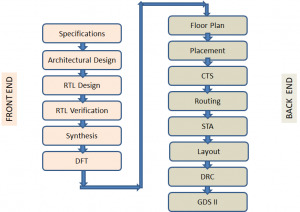
As it shows the design flow starts with a specification document which lists out the technical requirements needed in the chip design. It is followed by translating the specification to Architectural design. The architectural design involves designing the functional blocks and the communication protocol between them and translating them into actual modules that contain FSMs, combinational and sequential circuits etc. The architectural design is then modelled using a Hardware description language like Verilog/VHDL/System Verilog, which is the RTL design stage. The Functional Verification stage starts with a verification plan and a corresponding verification environment which describes and implements the method of proving the design correctness, using different Verification techniques. The design is refined until the HDL model is proved to be meeting the specifications.This stage is followed by Synthesis – a process of transforming the HDL design into a technology specific gate-level netlist, given all the specified constraints and optimization settings. DFT is a structural technique which facilitates a design to become testable after production. All the works till this stage are normally called as the Frontend of VLSI design and are executed by Frontend Engineers.
The next step in the ASIC Design flow is Placement and Routing which involves arranging approximate locations of a set of modules that need to be placed on a layout. Clock tree synthesis is a process which makes sure that the clock gets distributed evenly to all sequential elements in a design to fix the timing violations. This is followed by routing in which exact paths for the interconnection of standard cells and macros and I/O pins are determined.The file produced at the output of the layout is the GDSII (GDS2) file which is the file used by the foundry to fabricate the silicon. Gate level simulations and Static Timing Analysis (a method of validating the timing performance of a design by checking all possible paths for timing violations without having to simulate) are also done to make sure that the gate level design meets the timing requirements for correct design operations. All steps after logic synthesis are performed by Backend engineers and forms the Backend jobs.
Work of a Frontend Engineer
RTL Design/Coding
Synthesis
Functional Verification
DFT
Work of a Backend Engineer
Floor Planning
Placement
Clock Tree Synthesis
STA
Physical Verification
Which one has more career Opportunities?
With the advances being made in technologies like process geometries, feature size and product innovations on a daily basis, there is a constant need to design, develop and re-engineer integrated circuits (ICs). Since electronic products like mobile phones are being released with new features in shorter cycles, there is a healthy demand for qualified VLSI engineers to work on these products. Therefore, there is good scope for a career in the VLSI industry. The important point is that both the domains, front end and back end have their own advantages and have great career prospects. It is completely up to you which one to choose depending on your interest and confidence level, as both offer a great deal of learning and growth.
How to choose?
In order to become a front end engineer, one needs to have good knowledge of HDLs(Verilog/VHDL/SystemVerilog). It will be an added advantage if you have industry related protocol knowledge. So if you have ample digital fundamental knowledge, are fond of HDL coding, love debugging and want to have a sound understanding about the functionality of IC or chip you should definitely go for Front End. With the recent emergence of Artificial intelligence and its application towards VLSI opens up a huge scope for Front end engineers. In order to become a back end engineer, one needs to be well equipped with the concepts of digital electronics, CMOS and Analog Circuits, Scripting knowledge for automation, Hands on Tools for physical design, layout etc. If the above mentioned skills fascinates you then you can opt for Backend and there might be a chance to work in Foundry as well.
Challenges faced by a fresher to get into VLSI industry
Even though VLSI industry is a niche and has lots of career opportunities, on the flip side, industry is currently somewhat less reachable for fresh graduates, compared to other areas due to some particular reasons. Firstly, VLSI or chip design requires a deeper level of knowledge and skills than other electronics related fields .But our Universities are not catering 100% to the VLSI industry requirements. Secondly, VLSI chip design is expensive and requires access to high-cost, specialised electronic design automation (EDA) tools.
How can Chipedge help?
Chipedge offers various courses for fresh graduates both in frontend and backend domains, to choose from. The courses are well structured starting from building a strong foundation by emphasising on fundamental subjects like Digital, CMOS etc. Once the candidate becomes confident with the fundamental knowledge, we impart all the domain specific skills required for the VLSI industry, by giving hands on training on industry standard EDA tools (Synopsys).
1 note
·
View note
Photo

An introduction to the basic design flow in VLSI physical design automation, the basic data structures and algorithms used for executing the same is given to students. The course also provides examples and assignments making it easy for the participants to understand the concepts involved.
Website : https://www.rv-skills.com/vlsi-course/advanced-diploma-in-asic-design-physical-design.php
0 notes
Link
RV-VLSI is an integral part of RV-SKILLS that concerns itself with training in backend courses and job-oriented VLSI courses. At RV-VLSI, we offer a variety of programs to enable complete Skill Transformation - Advance Diploma in ASIC Design, Advanced Diploma in Embedded Systems (ADEMS), and Certificate courses available in full-time and part-time modes for students, graduates, post-graduates, professionals and corporates.
0 notes
Link
Best VLSI Placement| RV Skills | VLSI Placement Opportunities
0 notes