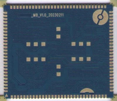
#printed circuit board assembly process flow
Explore tagged Tumblr posts
Visit Tumblr Blog
Explore Tumblr blogs with no restrictions, modern design and the best experience.
Last Seen Tumblr Blogs


Fun Fact
There were a total of 171.5 billion posts on Tumblr in 2019.
Text
Understanding the Functionality of Samsung Refrigerator PCB Main Assembly

Samsung refrigerators have become essential appliances in modern households, offering innovative features and advanced technologies to ensure food preservation and convenience. The (Printed Circuit Board) PCB Main Assembly serves as the brain of the refrigerator, coordinating various functions and ensuring optimal performance.
Components of the Refrigerator PCB Main Assembly
The Refrigerator PCB Main Assembly consists of several essential components, each playing a crucial role in the refrigerator's operation.
Microcontroller: It is the central processing unit (CPU) and the computer performs programmed instructions to coordinate communication between the components.
Sensors: The ambient parameters (temperature, humidity, door status) supply critical information for regulation.
Relays: You control the flow of electricity to the compressor, fan motors, and defrost heater.
Capacitors: It will help you store the electrical energy and help to regulate voltage, and guarantee that the PCB is operating reliably.
Resistors: Protect sensitive components from harm by limiting the flow of electricity across certain circuits.
Diodes: Allow current to flow exclusively in one direction to avoid reverse polarity and safeguard components from damage.
Connectors: Facilitate electrical connections between the PCB and other refrigerator components to ensure seamless integration.
Working Principle PCB Main Assembly
The PCB Main Assembly operates on a set of programmed instructions that determine its behavior depending on sensor input and user command. The micro controller continuously monitors sensor input such as the reading of the temperature from the refrigerator compartment, and freezer. The microcontroller controls the transition of the compressor on, or off or the speed of the fan and also the defrost cycles based on the sensor data as to how to keep the temperature and humidity at the optimal level. In addition to the other refrigerator components, for example, display panel and user interface, the PCB Main Assembly provides feedback and enables users’’ interaction. The PCB Main Assembly incorporates safety features of overload protection and temperature sensors to protect the refrigerator from damage and to protect the user.
Communication Protocols
Data can be communicated to other components through microcontrollers by communication protocols like UART (Universal Asynchronous Receiver Transmitter), SPI (Serial Peripheral Interface), and I2C (Inter Integrated Circuit).
UART is used to transfer real-time data from a microcontroller to external devices like display panels and temperature sensors.
There is a power of communication SPI and I2C for the communication of integrated circuits associated with the PCB Main Assembly for efficient data transfer and synchronization between components.
Troubleshooting and Maintenance
Common issues with the Samsung Refrigerator PCB Main Assembly include sensor failures, relay malfunctions, and power supply issues, which can affect the refrigerator's performance.
To solve PCB Main Assembly problems, we can use diagnostic methods, like running self-tests and checking the error code.
The assembly can stay longer depending on the main, such as cleaning dust and debris from the PCB and securing appropriate ventilation.
The PCB Main Assembly is an important component of the Samsung refrigerator systems since it organizes several functions to contribute to the overall efficiency of the refrigerator and food preservation. Fore-knowledge of the PCB Main Assembly and the way it is constructed can assist users in likely managing problems in their fridges.
2 notes
·
View notes
Text
Comprehensive Guide to PCB Board Design & Printed Circuit Assembly for Optimal Electronic Performanc
Compre
Modern electronics rely heavily on printed circuit boards (PCBs). Without well-designed PCBs and quality assembly, devices can become unreliable or fail prematurely. Whether you’re a designer or manufacturer, understanding how to create and assemble high-quality PCBs is crucial. This guide covers essential design principles, manufacturing methods, testing, and tips for better PCB performance.
Understanding PCB Board Design Fundamentals
The Role of PCB Design in Electronics Functionality
PCB design is the blueprint that shapes how your device works. It directly influences electrical signals, heat management, and overall durability. Poor design can lead to issues like signal interference or overheating, hurting the product's performance. Good design results in a more reliable, longer-lasting device that customers can count on.
Essential Components of a PCB Design
A PCB isn’t just a green board with some wires. It includes multiple elements such as:
Layers: These are the different sheets of the PCB, repeating signals or power.
Traces: Thin lines of copper that connect components.
Pads: Contact points for mounting parts like chips or resistors.
Vias: Small holes that link traces on different layers.
Components: Resistors, capacitors, ICs, and other parts attached to the board.
Each piece affects how well the circuit functions. Proper layout and placement ensure electrical signals flow smoothly and the device functions as intended.
Designing for Manufacturing (DFM) Best Practices
Designing with manufacturing in mind helps lower costs and speeds up production. Here are key tips:
Use standard component sizes and footprints.
Keep traces wide enough to handle current.
Avoid tiny vias or complex shapes that are hard to manufacture.
Place components logically to reduce assembly time.
Minimize the number of layers if possible. Fewer layers often mean lower costs.
These practices make it easier for factories to produce your design without errors or delays.
Types of Printed Circuit Boards and Their Applications
Rigid PCBs
Rigid PCBs are the most common type. They’re made of solid material, like fiberglass, that keeps the board stiff. You’ll find these in everything from computers to appliances. They’re reliable, cost-effective, and easy to handle during assembly.
Flexible and Rigid-Flex PCBs
Flexible PCBs bend and fold, fitting into small spaces inside devices. Rigid-flex combines both types, offering stiffness where needed and flexibility elsewhere. These are popular in wearable tech and smartphones, where space is tight.
High-Frequency and HDI PCBs
Special boards designed for fast signals — known as high-frequency PCBs — are used in radio, radar, and satellite systems. HDI (High-Density Interconnect) PCBs pack more components into less space, ideal for miniaturized electronics like medical devices or smartphones.
The Printed Circuit Assembly (PCA) Process
From Design to Production: Step-by-Step Overview
A typical PCA process includes:
Designing the circuit using CAD tools.
Verifying the design for errors.
Creating prototypes for testing.
Moving into full-scale manufacturing.
Assembling components via soldering.
At every step, quality checks are essential to prevent costly mistakes later.
Key Manufacturing Techniques
Surface-Mount Technology (SMT): Attaching components on the surface. It’s fast and suitable for high-volume production.
Through-Hole Assembly: Inserting pins into drilled holes. Best for parts needing full mechanical strength.
Automated Assembly: Robots place components quickly with high precision.
Manual Assembly: Used for small runs or complex parts, but slower.
Choosing the right method impacts the speed and quality of your PCB production.
Quality Control and Inspection
Regular inspections catch problems early:
X-ray Inspection: Checks hidden solder joints.
Automated Optical Inspection (AOI): Finds defects on the surface.
SPI (Solder Paste Inspection): Ensures correct solder paste volume.
Complying with standards like IPC-610 and IPC-2221 helps keep quality high and consistent.
Critical Factors Influencing PCB and PCA Quality
Material Selection for Durability and Performance
Choosing the right materials makes a difference:
Substrates like FR-4 are common but vary in quality.
Copper thickness affects current capacity.
Solder masks prevent shorts and corrosion.
Durable materials stand up to temperature, vibration, and environmental stress.
Design for Reliability
To keep your device working long-term:
Minimize electrical interference by proper grounding.
Manage heat by placing heat-sensitive parts away from heat sources.
Use clear labels and ample space for easy assembly and maintenance.
Good practice prevents failure and reduces warranty repairs.
Environmental Considerations
PCBs face many conditions:
Use conformal coatings to protect from moisture.
Choose vibration-resistant designs for mobile devices.
Select temperature-tolerant materials for harsh environments.
Designing for these factors enhances lifespan and performance.
Cost Optimization
Balancing quality with budget is key:
Use standard components rather than custom parts.
Avoid overly complex designs.
Optimize layout for easy assembly.
Good planning reduces waste and keeps costs in check.
Best Practices for PCB Design and Assembly Optimization
Design Tips for Ease of Assembly
Properly space components for automatic placement.
Use clear silkscreen labels to identify parts.
Keep copper traces away from component pads for easier soldering.
Simplicity saves time during manufacturing and reduces errors.
Enhancing Manufacturing Efficiency
Stick to standard footprints.
Avoid intricate shapes on copper traces.
Use consistent pad sizes and pad-to-component spacing.
This approach speeds up production and keeps quality high.
Post-Assembly Testing and Validation
Once assembled, testing is crucial:
Conduct functional testing to verify operation.
Use burn-in tests to detect early failures.
Carry out long-term stress tests for durability.
Thorough testing ensures your product withstands real-world use.
Collaborating with Proven PCB Manufacturers
Choose manufacturers with:
Certifications like IPC-6012 or ISO 9001.
Experience in your specific PCB type.
Good communication and ability to meet deadlines.
Partnering with reliable suppliers reduces risks and improves final product quality.
Case Studies and Real-World Examples
Some companies have achieved great results by focusing on PCB design. For example, an electronics firm reduced their device failure rate by improving trace routing and component placement. Conversely, poor design choices, such as crowded traces, led to short circuits and costly recalls. Learning from these stories highlights the importance of meticulous planning and quality control.
Conclusion
Creating a high-performance PCB, from design to assembly, is essential for reliable electronics. Focus on good design practices, choose the right materials, and work with experienced manufacturers. Regular testing and inspection help catch issues before products hit the market. As technology advances, keep an eye on trends like miniaturization and high-frequency PCBs. Staying current ensures your designs remain competitive and durable. Quality now means better devices, happier users, and fewer headaches later.
0 notes
Text
Navigating the Future of Electronics with Rigid-Flex and Taconic PCB Manufacturers
Today’s Printed Circuit Boards (PCBs) are much more flexible and advanced than the first rigid versions. Compact devices with great capabilities and multiple features have earned popularity in the electronics industry, leading to the rise of Rigid-Flex PCBs and Taconic PCBs. The use of these technologies enables unique designs, improves how long the device works, and maintains good electricity flow. Rigid-flex PCB Manufacturers can move and also keep their form, similar to how rigid boards function. They particularly shine in high-speed or RF and microwave applications. Dependable and effective products rely greatly on what electronics do.
Rigid-Flex PCBs: Hybrid Structure with High Functionality
Rigid-Flex PCBs take attributes from both stiff and flexible PCBs and merge them into one board. As a result, rigid and flexible boards no longer need connectors and cables, letting us make assemblies that are lighter and more space-saving. You can find these boards in smartphones, medical devices used on patients, military systems and aerospace devices. They are suited for use in places that require resistance to vibration and bending due to machines. In manufacturing, various layers are made and bonded together using very accurate methods. Therefore, it is only experienced manufacturing companies that can keep products of constant quality and performance.
Key Advantages of Rigid-Flex PCB Manufacturers
Important benefits of using well-known Rigid-flex PCB Manufacturers are their excellent design aid and advanced methodologies. They depend on laser direct imaging for precise work and optical inspection that finds problems in the early stage. Tests using temperature fluctuation and electrical overload guarantee that the product will function in any extreme condition. Manufacturers typically boost efficiency by assisting with design changes that lower the number of components and simplify assembly. In addition, they guarantee that flexible circuit boards meet all IPC standards for quality. Because they are involved in developing products and moving them into mass production, they help make the process more efficient.
Taconic PCBs: High-Frequency Performance Excellence
Taconic PCB Manufacturers are produced from proprietary PTFE-based laminates designed by Taconic with low dielectric loss and thermal stability. These boards are the preferred option for RF, microwave, and high-speed digital designs. They are most prevalent in satellite communications, radar systems, 5G base stations, and aerospace communication modules. Taconic laminates have low signal attenuation and superior dimensional stability. They exhibit moisture resistance as well as heat tolerance, which makes them dependable in extreme working environments. Production using these laminates demands proficiency in drilling, plating, and multilayer bonding because of their special properties.
What to Expect from a Taconic PCB Manufacturers
The best Taconic PCB Manufacturers must possess extensive experience in working with high-frequency laminate material. It involves strict impedance control, surface preparation, and low-loss transmission line engineering. Cleanroom facilities, specially designed PTFE-compatible equipment, and precise lamination procedures are necessary for high-quality output. The producers may perform RF testing and thermal profiling to ensure circuit integrity. They also guide customers on stack-up selection as well as PCB layout according to end-use frequency requirements. By maintaining compliance with IPC and MIL-spec specifications, these companies ensure the critical applications' performance and safety.
Comparing Rigid-Flex and Taconic PCBs
Although both are sophisticated PCBs, Rigid-Flex and Taconic PCBs are for different technical applications. Rigid-Flex is prized for mechanical flexibility, whereas Taconic leads for signal transmission at high speeds. Rigid-Flex boards simplify systems and minimize space utilization in cramped enclosures, while Taconic boards maintain signal purity in communication networks. The components and manufacturing methods are quite different, as are the final-use applications. The two are chosen based on physical space, frequency range, and exposure to the environment. Designers will often talk to both varieties of manufacturers to match their circuit requirements with the appropriate solution.
Conclusion
As innovation speeds up in electronics, the need for Rigid-flex PCB Manufacturers and Taconic PCBs keeps increasing. Such technologies facilitate the development of lighter, faster, and more efficient devices across industries. With increasingly sophisticated design challenges, collaborating with an experienced manufacturer is crucial. BS Interconn Hong Kong Co., LIMITED differentiates itself by providing quality-oriented, customer-centric PCB manufacturing services. Whether you're creating a next-generation medical wearable or a state-of-the-art RF device, selecting a reliable Rigid-Flex or Taconic PCB producer guarantees that your product will outperform and outlast the competition.
#Rigid-flex PCB Manufacturers#Taconic PCB Manufacturers#flexible circuit boards#high-frequency PCB#RF PCB solutions#microwave PCBs#PTFE laminates#hybrid PCB design#aerospace PCB#medical device PCBs#5G PCB manufacturer#signal integrity PCB#low dielectric PCB#high-speed PCB#multilayer PCB assembly#IPC compliant PCBs#MIL-spec PCBs#advanced PCB manufacturing#Taconic laminate PCB#Rigid-Flex technology
1 note
·
View note
Text
Why Are Surface Mount Inductors Vital in Modern Electronics? A Complete Guide

Surface mount inductors have emerged as critical components in today’s compact and high-performance electronic devices. As the demand for miniaturization and efficiency continues to grow, these components offer a reliable solution for energy storage, filtering, and signal integrity. Whether you are designing consumer electronics, industrial systems, or automotive applications, understanding the role and advantages of surface mount inductors can significantly enhance your product development process.
What Are Surface Mount Inductors?
Surface mount inductors are passive electronic components designed to store energy in a magnetic field when electrical current flows through them. Unlike traditional through-hole inductors, surface mount variants are mounted directly onto the surface of a printed circuit board (PCB), enabling compact, low-profile, and automated assembly designs. These inductors are widely used for their efficient space utilization and high-frequency performance.
How Do Surface Mount Inductors Work?
The basic working principle of surface mount inductors is grounded in electromagnetic induction. When current passes through the coil inside the inductor, it creates a magnetic field. This field resists changes in the current, providing a filtering or energy storage function depending on the application.
Surface mount inductors are typically manufactured using a ferrite or powdered iron core surrounded by a coiled conductor. The magnetic properties of the core and the number of coil turns determine the inductance value. Their compact design allows them to perform reliably in dense circuit boards.
Where Are Surface Mount Inductors Used?
These inductors are essential in multiple sectors where space-saving components are crucial. Common applications include:
Smartphones, tablets, and laptops
Power supplies and DC-DC converters
Automotive electronic control units (ECUs)
RF and telecommunications systems
Medical and industrial instrumentation
LED lighting systems and IoT modules
Each of these areas requires high-performance signal integrity and energy efficiency, both of which are facilitated by surface mount inductors.
What Are the Key Benefits of Surface Mount Inductors?
Surface mount inductors provide a range of advantages for engineers and product designers. Their integration into compact electronics is particularly valuable in today’s market.
Enable miniaturized circuit design for compact devices
Support high-frequency operations with excellent performance
Reduce production time through automated pick-and-place mounting
Offer low DC resistance (DCR) for higher efficiency
Enhance electromagnetic compatibility (EMC) in sensitive circuits
Provide thermal stability in harsh environments
Available in a wide variety of inductance values and sizes
These benefits make them indispensable in both analog and digital electronic systems.
What Are the Different Types of Surface Mount Inductors?
The choice of surface mount inductor depends on the specific application and performance requirements. Key types include:
Wire-wound inductors: Known for high Q-factor and current handling capabilities, ideal for power applications.
Multilayer inductors: Offer compact size and are suitable for high-frequency filtering.
Thin-film inductors: Deliver precision and low-profile characteristics, often used in RF circuits.
Molded inductors: Provide strong mechanical durability, often used in automotive environments.
Each type has unique characteristics that influence its behavior in a circuit, and selecting the right one depends on factors such as frequency, current rating, and size constraints.
How to Choose the Right Surface Mount Inductor?
Selecting the right surface mount inductor for your application involves considering several important technical parameters:
Inductance (L): Measured in microhenries (µH) or nanohenries (nH), this value defines how much energy the inductor can store.
Current rating: Determines the maximum current the inductor can handle without saturating or overheating.
Saturation current: Indicates the point at which the inductor loses its inductive properties.
DC resistance (DCR): Lower DCR means better efficiency and less power loss.
Frequency range: Ensures compatibility with the intended signal or switching frequency.
Size and footprint: Must match the PCB layout and spatial constraints.
Understanding these parameters helps ensure optimal circuit performance, reliability, and compliance with regulatory standards.
Why Are Surface Mount Inductors Preferred Over Through-Hole Types?
While both surface mount and through-hole inductors serve similar electrical purposes, surface mount options are increasingly preferred in modern electronic assemblies. This shift is driven by:
Smaller package sizes suitable for compact PCBs
Better performance at higher frequencies
Faster, more cost-effective automated manufacturing
Improved thermal performance in high-density applications
Enhanced mechanical stability during vibration or movement
Surface mount technology enables the design of lightweight, efficient, and high-performance devices across various industries.
What Are the Trends in Surface Mount Inductor Technology?
As technology evolves, surface mount inductors continue to improve in performance, durability, and miniaturization. Key developments in this field include:
Use of advanced core materials for higher energy density
Lower EMI solutions to support 5G and wireless technologies
Integration with ICs and other passives for modular designs
Eco-friendly manufacturing with lead-free soldering
High-reliability solutions for automotive and aerospace sectors
These innovations make surface mount inductors a forward-looking solution for next-generation electronic products.
Where to Buy High-Quality Surface Mount Inductors?
Finding trusted suppliers is essential for securing reliable surface mount inductors. It’s important to source components from distributors that provide:
Comprehensive technical datasheets
RoHS-compliant and quality-certified components
Wide inventory of top brands and value options
Global shipping and responsive customer service
Compatibility with high-frequency and power electronics
Buyers and engineers should consider trusted electronic suppliers with extensive product listings and verified sourcing standards.
Conclusion
Surface mount inductors are indispensable building blocks of today’s advanced electronic systems. Their compact form factor, high-frequency capability, and reliable performance make them ideal for power conversion, signal conditioning, and EMI suppression tasks. By understanding how these components work, where they are used, and how to select the right one, engineers can unlock new possibilities in their designs. As innovation accelerates, surface mount inductors continue to play a central role in enabling smarter, smaller, and more efficient electronics.
0 notes
Text
Analysis of the Causes of Component Displacement in SMT Assembly Production and Handling Methods
With the development of technology and the improvement of living standards, the pursuit of electronic products is increasingly trending towards miniaturization and precision. In SMT small-batch patching processing plants, traditional DIP plug-ins no longer play as significant a role in small, compact PCBA as SMT patching, especially for large-scale and highly integrated ICs. The precision industry requires meticulous attention to both material usage and processing steps, as even the slightest error can render the entire device inoperable. Therefore, every step in the patching process must be carefully observed.
SMT patching processing, namely Surface Mount Technology (SMT), is the most popular technology and process in the current electronic assembly industry. Surface Mount Technology for electronic circuits, also known as surface mounting or surface installation technology, primarily aims to accurately mount surface-mounted components onto fixed positions of a PCB. However, during patching processing, some process issues may arise, affecting patching quality—such as component displacement. Component displacement in patching processing is a precursor to several other problems during the welding process and requires attention. So, what are the causes of component displacement in patching processing?
Causes of Component Displacement in Patching Processing:
Solder paste has a limited shelf life. After exceeding the usage period, the flux in it deteriorates, leading to poor soldering.
The solder paste itself has insufficient viscosity, causing component displacement due to oscillations or shaking during handling.
Excessive flux content in the solder paste leads to component displacement due to the flow of excess flux during reflow soldering.
Component displacement caused by vibration or improper handling during transportation after printing and patching.
In patching processing, the suction nozzle's air pressure is not adjusted properly, with insufficient pressure causing component displacement.
Mechanical issues with the patching machine itself result in incorrect component placement.
Once component displacement occurs in patching processing, it affects the circuit board's performance. Therefore, during processing, it is necessary to understand the causes of component displacement and address them specifically.
Targeted Solutions Based on Specific Causes:
Strictly calibrate positioning coordinates to ensure the accuracy of component mounting.
Use high-quality, high-adhesion solder paste to increase SMT mounting pressure and bonding force for components.
Select appropriate solder paste to prevent solder paste collapse, with the solder paste having a suitable flux content.
Adjust the speed of the fan motor.
In fact, in the reflow soldering of SMT patching processing, besides component displacement, there are many other possible defects, such as stand-up and flip-over issues. However, these defects can be resolved by starting from circuit board design—from excellent PCB fabrication to meticulous execution in responsible SMT patching processing—addressing everything from components to solder paste and processes to fundamentally improve reflow soldering quality and prevent component displacement.
Want to know more? Contact me at [email protected]. From Sandy
0 notes
Text
How Can Flux Boost Solder Joint Reliability in Electronic Soldering?
Soldering is a cornerstone of electronics manufacturing, especially when connecting metals in printed circuit board (PCB) assembly, where flux is vital for achieving solder joint reliability. This reliability ensures that joints withstand daily wear, environmental stress, and mechanical strain without cracking or failing. This guide explores the types of flux available, their benefits and limitations, and flux removal methods, all tailored to enhance solder joint reliability in electronic products.
Flux facilitates soldering and desoldering by removing oxide layers, improving solder wetting, and ensuring even flow—key factors in achieving solder joint reliability. In electronic soldering, flux promotes robust connections between components, critical for solder joint reliability. Soldering uses a molten alloy, or solder, to bond metal surfaces, but impurities, oxides, and contaminants can undermine solder joint reliability. Flux counters these issues by cleaning surfaces, enabling strong, dependable metallurgical bonds essential for long-term solder joint reliability.

Understanding Flux and Its Role in Solder Joint Reliability
Flux is a compound that prepares metal surfaces for soldering by removing oxides, promoting wetting, and enhancing solder flow—all crucial for solder joint reliability. Available as paste, liquid, or within solder wire cores, flux contains active agents like rosin or organic acids that react with surface oxides. When heated, flux activates, clearing oxides to prevent interference, directly supporting solder joint reliability. By reducing solder surface tension, flux ensures uniform spreading, forming joints that bolster solder joint reliability.
Moreover, flux forms a protective barrier during soldering, preventing oxide reformation and preserving solder joint reliability by shielding cleaned surfaces from atmospheric oxygen. This protection is vital for maintaining clean, consistent joints that ensure solder joint reliability in electronic applications. For advanced soldering processes, equipment like the Vacuum Soldering System KD-V200HT can further enhance this process by providing a controlled vacuum environment, minimizing oxidation and improving solder joint reliability. The KD-V200HT is particularly effective for high-precision applications where maintaining a pristine soldering environment is critical.
Types of Flux and Their Impact on Solder Joint Reliability
Different flux types address varying soldering needs, each influencing solder joint reliability based on their formulation and activity level. Some target specific metals like copper, while others offer versatility, with activity ranging from mild to highly active depending on oxidation levels affecting solder joint reliability.
IPC J-Standard Flux Classification for Solder Joint Reliability
The IPC J-Standard classifies flux by composition and activity, a system critical for ensuring solder joint reliability in modern electronics. Categories include Rosin (RO), Organic (OR), Inorganic (IN), and Resin/Synthetic Resin (RE), with activity levels of Low (L, <0.5% halide), Moderate (M, 0-2% halide), or High (H, >2% halide). Halide content (Cl- or Br-) splits them into 0 (no halide) or 1 (some halide). For instance, ROL0 is a low-activity, halide-free rosin flux ideal for basic solder joint reliability, while ROM1 (e.g., RMA with 0.5-2% halide) offers moderate activity for more challenging solder joint reliability needs.
Rosin (R-Type) Flux and Solder Joint Reliability
Rosin flux, derived from pine tar resin, is a traditional choice for soldering, leveraging natural acids like abietic acid to enhance solder joint reliability. In its basic R-type form, rosin dissolved in solvents like isopropyl alcohol lacks activators, suiting simple tasks where solder joint reliability is less demanding. For tougher oxides—common with lead-free alloys at higher temperatures—activators create Rosin Mildly Activated (RMA) or Rosin Activated (RA) fluxes. These include organic acids, halides, or salts, boosting solder joint reliability by tackling heavy oxide layers.
However, activated rosin fluxes can leave corrosive residues like chloride ions, threatening solder joint reliability if not removed post-soldering. These tacky remnants may attract conductive dust, risking short circuits and undermining solder joint reliability. With lead-free soldering’s rise, higher temperatures necessitate active fluxes, making thorough cleaning critical for sustained solder joint reliability. For lead-free soldering, the Inline Void-Free Reflow Oven for Diode KD-V10S HVT can be a game-changer. The KD-V10S HVT reduces voids in solder joints, directly contributing to improved solder joint reliability by ensuring consistent bonding at elevated temperatures.
No-Clean Flux and Solder Joint Reliability
No-clean fluxes, using rosin or synthetic resins, aim to simplify processes while supporting solder joint reliability. Rosin-based versions have lower rosin content than R-type fluxes, while synthetic options mimic rosin’s properties. Though some include mild activators, residues can still affect solder joint reliability if corrosive.
Designed to minimize cleanup, no-clean fluxes leave less residue than R-type fluxes, typically insufficient to disrupt solder joint reliability or cause corrosion over time. Yet, sticky residues may attract dust, impacting aesthetics or solder joint reliability in sensitive applications. For conformal coating, even minimal residue must be removed to ensure coating adhesion and preserve solder joint reliability. With lead-free alloys requiring active fluxes, cleanup may still be needed, potentially offsetting no-clean benefits for solder joint reliability. In such cases, using the Vacuum Reflow Soldering Oven KD_V10N HVT can help. The KD_V10N HVT offers precise temperature control in a vacuum environment, reducing residue issues and enhancing solder joint reliability for lead-free soldering applications.
Water-Soluble Flux and Solder Joint Reliability
Water-soluble fluxes, often resin-based, require water rinsing to remove residues, directly impacting solder joint reliability. Some are water-based, reducing VOC emissions—a plus for eco-conscious manufacturers aiming for solder joint reliability under strict regulations. Activators like organic acids or halides, while effective, are corrosive, necessitating removal to safeguard solder joint reliability over time.
Flux Formats and Their Contribution to Solder Joint Reliability
Flux comes in various formats—liquid, tacky, flux-cored solder, and solder paste—each enhancing solder joint reliability based on application needs and soldering methods.
Liquid Flux: Applied via bottles, syringes, or pens, liquid flux cleans surfaces before soldering, improving flow and ensuring solder joint reliability. It’s vital in wave soldering, where precise application via spray or foam supports consistent solder joint reliability.
Tacky Flux: With a gel-like consistency, tacky flux adheres to surfaces, ideal for vertical joints where maintaining position enhances solder joint reliability.
Flux-Cored Solder: Combining solder and flux in a wire core, this format cleans surfaces as it melts, streamlining processes and bolstering solder joint reliability.
Flux in Solder Paste: Used in surface-mount technology (SMT), solder paste integrates flux with alloy particles, securing components and promoting solder joint reliability during reflow. For SMT applications, the Inline Vacuum Soldering Systems KD_V400 can optimize the reflow process. The KD_V400 ensures uniform heating and a controlled vacuum environment, which minimizes defects and improves solder joint reliability in SMT soldering.
Ensuring Solder Joint Reliability Through Flux Selection and Advanced Equipment
Flux is indispensable for solder joint reliability, removing oxides, enhancing wetting, and preventing re-oxidation. These functions create robust joints critical for electronic performance. Choosing the right flux—rosin, no-clean, or water-soluble—optimizes solder joint reliability by matching the soldering task’s demands. For instance, RMA flux suits lead-free soldering where oxide removal is key to solder joint reliability, while no-clean flux supports quick assembly with minimal cleanup, assuming residues don’t compromise solder joint reliability.
Advanced equipment can further enhance solder joint reliability. For power module applications requiring precise bonding, the Inline 4-Chambers Vacuum Soldering Oven with Formic Acid KD-V400L provides a controlled environment that reduces defects. The KD-V400L uses formic acid to further clean surfaces during soldering, ensuring solder joint reliability by minimizing oxidation and supporting consistent joint quality in high-power applications.
Post-soldering flux removal is equally critical for solder joint reliability. Corrosive residues from activated fluxes must be cleaned to prevent long-term degradation, ensuring solder joint reliability in harsh environments. Even no-clean fluxes may require removal for aesthetic or coating purposes, reinforcing solder joint reliability in high-stakes applications.
Conclusion
Flux underpins solder joint reliability in electronic soldering, enabling clean, strong connections that withstand operational stresses. By selecting appropriate flux types and formats—whether rosin for traditional needs, no-clean for efficiency, or water-soluble for eco-friendliness—and leveraging advanced equipment like the Vacuum Soldering System KD-V200HT, Inline Void-Free Reflow Oven for Diode KD-V10S HVT, Vacuum Reflow Soldering Oven KD_V10N HVT, Inline Vacuum Soldering Systems KD_V400, and Inline 4-Chambers Vacuum Soldering Oven with Formic Acid KD-V400L, manufacturers can enhance solder joint reliability across PCB assembly and beyond. Proper flux management, including residue removal where necessary, ensures that solder joint reliability remains uncompromised, delivering durable, high-performing electronic products in 2025 and beyond.
#donald trump#asexual#easter#michael cera#artists on tumblr#rwby#margot robbie#barbie#across the spiderverse#ryan gosling
0 notes
Text
How to Overcome Common Challenges in PCB Assembly for ESDM Projects

In the dynamic world of Electronics System Design and Manufacturing (ESDM), success hinges not just on innovation, but also on precise execution—especially during PCB (Printed Circuit Board) assembly. As projects become more complex, so do the challenges faced during this critical phase. At Aimtron, we’ve seen firsthand how addressing these challenges early leads to smoother project flows, faster time-to-market, and higher quality products.
In this blog, we’ll dive into the most common PCB assembly challenges for ESDM projects and share proven strategies to overcome them.
1. Component Sourcing and Availability
The Challenge: Global supply chain disruptions, component shortages, and long lead times can delay PCB assembly, jeopardizing project timelines.
The Solution:
Early BOM Finalization: Lock your Bill of Materials (BOM) early and validate components for availability.
Multiple Sourcing Strategies: Partner with trusted suppliers and maintain alternate part options.
Inventory Management: Use just-in-time (JIT) inventory systems while keeping a buffer for critical components.
Leverage Aimtron’s Global Network: Our established supplier partnerships help mitigate shortages and ensure timely procurement.
2. Design for Manufacturability (DFM) Issues
The Challenge: PCBs designed without considering manufacturing capabilities often lead to rework, delays, and higher costs.
The Solution:
Early DFM Review: Engage manufacturing experts during the design phase for feedback on layout, spacing, and assembly feasibility.
Simulation and Validation: Use advanced tools to simulate manufacturing processes.
Collaboration with Aimtron's Engineering Team: Our design-for-assembly (DFA) and DFM services ensure your PCB designs are optimized for production from day one.
3. Soldering Defects
The Challenge: Soldering errors like cold joints, bridging, and voids can compromise the reliability of PCBs.
The Solution:
Precision Process Control: Strictly monitor solder paste application, reflow profiles, and hand-soldering techniques.
Quality Training: Continuous training of assembly staff in IPC standards.
Automated Optical Inspection (AOI): Aimtron uses AOI and X-ray inspection systems to detect and correct soldering issues in real-time.
4. Electrostatic Discharge (ESD) Damage
The Challenge: ESD can silently destroy sensitive electronic components during handling and assembly.
The Solution:
Strict ESD Protocols: Implement ESD-safe workstations, grounding systems, and employee training.
Continuous Monitoring: Use ESD monitoring devices to ensure protection throughout the facility.
Certified ESD-Safe Facilities: At Aimtron, our facilities meet global ESD standards to protect your PCBs during every step of assembly.
5. Maintaining Quality in High-Mix, Low-Volume Production
The Challenge: ESDM often requires the assembly of many different PCBs in small batches, making consistency a challenge.
The Solution:
Flexible Manufacturing Systems: Deploy agile production lines capable of quick changeovers.
Strong Documentation Practices: Use detailed work instructions and traceability systems.
Continuous Improvement Programs: Aimtron’s commitment to Kaizen ensures quality is never compromised, no matter the batch size.
6. Thermal Management During Assembly
The Challenge: Components that generate significant heat or require special handling (e.g., BGAs, high-power ICs) can complicate the assembly process.
The Solution:
Proper Heat Profiling: Develop accurate reflow oven profiles tailored to PCB thermal characteristics.
Use of Thermal Reliefs: Design PCBs with thermal relief pads to assist in proper soldering.
Thermal Simulation: At Aimtron, we utilize advanced modeling to predict and manage thermal challenges during assembly.
Conclusion
Navigating the complexities of PCB assembly in ESDM projects requires more than technical know-how—it demands a strategic, proactive approach. From sourcing components to ensuring ESD protection and optimizing for manufacturability, every step is critical.
At Aimtron, we don’t just assemble PCBs—we partner with you to engineer success at every stage of your ESDM journey. By combining cutting-edge technology, global resources, and a deep commitment to quality, we help you overcome challenges and deliver products that meet and exceed market expectations.
Need support for your next ESDM project? Contact Aimtron today and experience the difference that expertise makes.
#PCB Assembly#ESDM#Electronics System Design and Manufacturing#PCB Assembly Services#PCB Assembly Solutions#PCB Design
0 notes
Text
Minimize Design Iterations with PCB-Driven Mechanical Modeling
When it comes to product development, one thing’s clear—every iteration costs time. And in today’s fast-moving market, time is everything. That’s where PCB-driven mechanical modeling steps in to smooth out the bumps before they become costly detours.
This approach doesn’t just reduce revisions—it helps teams design smarter from day one. If you’re looking to tighten workflows and avoid unnecessary back-and-forth, this might just be your new favorite strategy.
Let’s break it down.
🚀 What Is PCB-Driven Mechanical Modeling?

In simple terms, it’s the integration of your Printed Circuit Board (PCB) layout into the mechanical CAD environment—early and accurately.
Instead of designing the enclosure and board in silos, the two are brought together right from the start. That means fewer surprises later.
No more, “Oh no, the USB port doesn’t line up,” or “Wait, there’s interference with that component.”
This is especially important in Mechanical & Thermal Design, where space, airflow, and structure must work in harmony with the electronics.
🧩 Why It Reduces Iterations
Traditional workflows often mean:
The electrical team finishes the PCB layout
The mechanical team gets it later
Changes and corrections begin...
Sound familiar?
With PCB-driven modeling, mechanical constraints like fit, clearance, airflow, and mounting can be addressed as the board is being laid out. You’re not designing in the dark.
In short, you:
Catch conflicts early
Avoid rework
Save valuable time
This keeps the Mechanical & Thermal Design process efficient, collaborative, and focused on results.
🛠️ Key Benefits of This Approach
1. Better Fitment, Fewer Surprises
All parts—screws, standoffs, connectors—can be placed with confidence. No last-minute enclosure redesigns.
2. Improved Thermal Planning
Heat-generating components can be positioned for optimal airflow and cooling solutions can be integrated without guesswork. That’s a big win for any Mechanical & Thermal Design process.
3. Streamlined Collaboration
Designers and engineers speak the same visual language when everything is modeled together.
4. Faster Time to Prototype
Less rework means quicker decisions, which leads to faster prototyping and testing.
🔄 Real-World Application: How It Fits Into the Workflow
Here’s how it usually plays out:
PCB layout starts with basic mechanical guidelines.
Mechanical model imports that layout and applies accurate dimensions, hole placements, and component heights.
Design teams collaborate in real-time to optimize the enclosure and internal spacing.
Thermal and structural simulations can now be run on a near-final assembly—before the first prototype is even made.
That tight loop is where the magic happens. It gives the Mechanical & Thermal Design process clarity and confidence.
🌬️ Don’t Forget Thermal
PCB-driven modeling also sets the stage for thermal analysis.
When component locations are fixed early, it’s easier to simulate heat flow and explore solutions like:
Heatsinks
Thermal pads
Air vents
Fans
This proactive mindset is what separates smooth launches from frustrating delays.
And yes, it’s a big part of modern Mechanical & Thermal Design strategies.
👀 Scannable Summary
What it is: Real-time mechanical modeling using actual PCB layout data
Why it matters: Reduces design iterations, errors, and rework
Top benefits: Better fit, faster prototyping, smarter thermal planning
Big picture: Aligns electrical and mechanical teams early in the process
Key use: Enhancing overall Mechanical & Thermal Design efficiency
✨ Final Thoughts
PCB-driven mechanical modeling isn’t just another box to tick—it’s a smarter way to work. When mechanical and electrical design speak the same language from day one, everything flows smoother.
And in a world where every iteration counts, that kind of alignment makes all the difference.
Whether you're designing a wearable, a power device, or an embedded system, this approach keeps your Mechanical & Thermal Design process on track—and your headaches to a minimum.
❓FAQs
Q1: Is PCB-driven modeling only useful for complex products?
Not at all. Even small devices benefit from early mechanical integration, especially when space is limited or thermal performance matters.
Q2: Does this replace traditional design methods?
No, it enhances them. It complements standard workflows by reducing manual back-and-forth and aligning teams earlier in the cycle.
Q3: What tools are typically used?
Mechanical CAD tools that support PCB import or integration, as well as simulation tools used in Mechanical & Thermal Design, are commonly used. The key is compatibility and collaboration.
0 notes
Text
PCB Assembly: A Comprehensive Guide to the Process and Benefits
Introduction
PCB Assembly is a critical step in the manufacturing of electronic devices. It involves mounting and soldering electronic components onto a printed circuit board (PCB) to create a functional unit. Whether for consumer electronics, industrial machinery, or medical devices, PCB Assembly ensures that circuits operate as intended.
This guide explores the PCB Assembly process, its key stages, benefits, and applications. By understanding how PCB Assembly works, businesses and engineers can optimize their production for better performance and reliability.
What Is PCB Assembly?
PCB Assembly refers to the process of attaching electronic components to a PCB. The assembled board, known as a PCBA (Printed Circuit Board Assembly), forms the core of most electronic devices. The process requires precision, as even minor errors can lead to circuit failure.
Key Components in PCB Assembly
Printed Circuit Board (PCB): The base that holds components and provides electrical connections.
Electronic Components: Resistors, capacitors, integrated circuits (ICs), and connectors.
Solder: A metal alloy that creates electrical and mechanical bonds between components and the PCB.
Flux: A chemical cleaning agent that improves solder flow and prevents oxidation.
The PCB Assembly Process
The PCB Assembly process consists of several stages, each crucial for ensuring a functional and reliable end product.
1. Solder Paste Application
Before placing components, solder paste is applied to the PCB pads using a stencil. The paste consists of tiny solder balls suspended in flux, which helps in bonding components to the board during reflow soldering.
2. Component Placement
Automated machines (pick-and-place robots) or manual labor position components onto the PCB. Surface-mount technology (SMT) is commonly used for small components, while through-hole technology (THT) is preferred for larger, more durable parts.
3. Reflow Soldering
The PCB passes through a reflow oven, where controlled heating melts the solder paste, creating permanent connections. The temperature profile must be carefully managed to prevent defects like cold joints or component damage.
4. Inspection and Quality Control
Automated Optical Inspection (AOI) and X-ray inspection check for misaligned components, solder bridges, or insufficient solder. Manual inspections may also be conducted for critical assemblies.
5. Through-Hole Component Insertion (If Applicable)
For THT components, leads are inserted into pre-drilled holes, and wave soldering secures them in place.
6. Final Testing
Functional testing ensures the assembled PCB operates correctly. Tests may include power-on checks, signal verification, and environmental stress screening.
Types of PCB Assembly
Different projects require different PCB Assembly techniques. The main types include:
1. Surface-Mount Technology (SMT) Assembly
Ideal for small, high-density components.
Faster and more cost-effective for mass production.
Requires precise machinery for accurate placement.
2. Through-Hole Technology (THT) Assembly
Better for larger, high-power components.
Provides stronger mechanical bonds.
Often used in military and aerospace applications.
3. Mixed Assembly (SMT + THT)
Combines both technologies for complex designs.
Offers flexibility in component selection.
Benefits of Professional PCB Assembly
Outsourcing PCB Assembly to experts offers several advantages:
1. High Precision and Consistency
Automated assembly reduces human error, ensuring uniformity across multiple units.
2. Faster Production
Advanced machinery speeds up the process, reducing lead times.
3. Cost Efficiency
Bulk production lowers per-unit costs, making it economical for large orders.
4. Improved Reliability
Professional assembly minimizes defects, enhancing product lifespan.
5. Compliance with Industry Standards
Certified manufacturers adhere to IPC and ISO standards, ensuring quality and safety.
Applications of PCB Assembly
PCB Assembly is used across various industries, including:
1. Consumer Electronics
Smartphones, laptops, and home appliances rely on PCB Assembly for functionality.
2. Automotive Industry
Engine control units (ECUs), infotainment systems, and sensors use assembled PCBs.
3. Medical Devices
Pacemakers, MRI machines, and diagnostic equipment require high-reliability PCBAs.
4. Industrial Automation
Robotics, control systems, and IoT devices depend on precision-assembled PCBs.
5. Aerospace and Defense
Avionics, radar systems, and communication devices use rugged PCB assemblies.
Choosing the Right PCB Assembly Partner
Selecting a reliable PCB Assembly service provider is crucial for success. Consider the following factors:
1. Experience and Expertise
Look for companies with a proven track record in your industry.
2. Advanced Equipment
Ensure they use modern SMT and THT assembly machines.
3. Quality Certifications
Check for ISO, IPC, and other relevant certifications.
4. Turnaround Time
Fast production and delivery times can impact project deadlines.
5. Customer Support
A responsive team helps resolve issues quickly.
Future Trends in PCB Assembly
The PCB Assembly industry continues to evolve with new technologies:
1. Miniaturization
Smaller components and high-density interconnects (HDI) enable compact designs.
2. Automation and AI
AI-driven inspection and robotic assembly improve accuracy and efficiency.
3. Eco-Friendly Practices
Lead-free soldering and recyclable materials support sustainability.
4. Flexible and Rigid-Flex PCBs
Growing demand for bendable circuits in wearables and medical devices.
Conclusion
PCB Assembly is a vital process in electronics manufacturing, ensuring that devices function correctly and reliably. By understanding the assembly stages, benefits, and applications, businesses can make informed decisions when selecting manufacturing partners.
As technology advances, PCB Assembly will continue to play a key role in innovation, enabling smarter, faster, and more efficient electronic products. Whether for prototyping or mass production, high-quality PCB Assembly remains essential for success in the electronics industry.
1 note
·
View note
Text
Wave Solder Bars for Electronics Manufacturing
In the world of electronics manufacturing, soldering is a critical process that ensures the reliability and functionality of electronic assemblies. Among the various soldering techniques, wave soldering stands out as a highly efficient method for mass-producing printed circuit boards (PCBs). A key component in this process is the wave solder bar, which plays a vital role in creating a consistent and high-quality solder joint.
This article explores the importance of wave solder bars for electronics manufacturing, their composition, types, benefits, and best practices for optimal performance.
What Are Wave Solder Bars?
Wave solder bars are metallic alloys used in wave soldering machines to create a molten solder wave that bonds electronic components to PCBs. These bars are melted in a solder pot, and a pump generates a wave-like flow of liquid solder, allowing the PCB to pass over it and form secure electrical connections.
The composition of wave solder bars typically includes a mix of tin (Sn) and lead (Pb), though lead-free alternatives have become more common due to environmental regulations such as RoHS (Restriction of Hazardous Substances).
Types of Wave Solder Bars
Different soldering applications require specific solder alloy compositions. Below are the most common types of wave solder bars used in electronics manufacturing:
1. Tin-Lead (Sn-Pb) Solder Bars
Traditional and widely used in the past.
Typically composed of 63% tin and 37% lead (eutectic mixture).
Offers excellent wetting properties and low melting point (183°C).
Gradually being phased out due to lead toxicity concerns.
2. Lead-Free Solder Bars
Compliant with RoHS and other environmental regulations.
Common alloys include:
Tin-Silver-Copper (Sn-Ag-Cu or SAC) – Popular for its reliability.
Tin-Copper (Sn-Cu) – Cost-effective but requires higher temperatures.
Tin-Silver (Sn-Ag) – Used in high-reliability applications.
Higher melting points (217–227°C) compared to Sn-Pb.
3. Specialty Solder Bars
Some applications require additives like nickel (Ni) or bismuth (Bi) to improve thermal cycling performance.
Used in high-stress environments such as automotive or aerospace electronics.
Benefits of Using High-Quality Wave Solder Bars
Using the right wave solder bars for electronics manufacturing ensures:
1. Strong and Reliable Solder Joints
Proper alloy selection minimizes defects like cold joints or bridging.
Ensures long-term durability of electronic assemblies.
2. Improved Wetting and Flow Characteristics
High-quality solder bars enhance solder flow, reducing voids and incomplete connections.
3. Compliance with Industry Standards
Lead-free solder bars meet environmental and safety regulations.
4. Cost Efficiency
Reduces rework and defects, lowering production costs.
Best Practices for Using Wave Solder Bars
To maximize the efficiency of wave soldering, manufacturers should follow these best practices:
1. Selecting the Right Alloy
Choose based on PCB type, component sensitivity, and regulatory requirements.
2. Maintaining Optimal Solder Temperature
Too high can damage components; too low leads to poor wetting.
Lead-free alloys require higher temperatures than Sn-Pb.
3. Regular Solder Pot Maintenance
Remove dross (oxidized solder) to prevent contamination.
Check for impurities that can affect joint quality.
4. Proper Flux Application
Flux removes oxidation and improves solder adhesion.
Use no-clean or water-soluble flux depending on cleaning requirements.
5. Monitoring Solder Bar Impurities
Excessive copper or other contaminants can weaken joints.
Regular testing ensures consistent solder quality.
Common Challenges and Solutions in Wave Soldering
Despite its advantages, wave soldering can face issues that affect product quality:
1. Solder Bridging
Cause: Excess solder or incorrect PCB design.
Solution: Adjust wave height and optimize pad spacing.
2. Cold Solder Joints
Cause: Insufficient heat or contamination.
Solution: Ensure proper preheating and clean PCB surfaces.
3. Dross Formation
Cause: Oxidation of molten solder.
Solution: Use nitrogen blankets to reduce oxidation and skim dross regularly.
4. Tombstoning (Component Lifting)
Cause: Uneven heating or incorrect pad design.
Solution: Balance thermal mass and adjust solder wave contact time.
Future Trends in Wave Soldering Technology
As electronics manufacturing evolves, so does wave soldering technology. Key advancements include:
1. Enhanced Lead-Free Alloys
Research focuses on improving thermal and mechanical properties.
2. Automation and AI Integration
Smart soldering systems adjust parameters in real-time for better consistency.
3. Eco-Friendly Fluxes and Processes
Reduced chemical waste and energy-efficient soldering techniques.
Conclusion
Wave solder bars for electronics manufacturing are essential for producing reliable and high-performance PCB assemblies. By selecting the right alloy, maintaining proper soldering conditions, and addressing common challenges, manufacturers can achieve superior solder joints while complying with industry standards.
As technology advances, innovations in wave soldering will continue to enhance efficiency, sustainability, and quality in electronics production. Investing in high-quality wave solder bars and best practices ensures long-term success in the competitive electronics manufacturing industry.

1 note
·
View note
Text
PCB Assembly SMT SMT process details
SMT (Surface Mounted Technology, Surface Mount Technology) is a pinless or short lead surface assembly components (SMC / SMD, that is, sheet components) directly mounted on the surface of the PCB (printed circuit board), and through the re-flow soldering or dip soldering and other methods to achieve the soldering and assembly of the circuit mounting technology. The following is a detailed introduction to the PCB assembly SMT SMD process:

First, the basic flow of the SMT placement process
Incoming material inspection
Inspection of the PCB board, to see if there is deformation, scratches, short circuit, open circuit and other issues, while checking the solder resist layer, silk screen layer and so on whether it meets the requirements.
The appearance, size, pin coplanarity of electronic components are tested to ensure that their quality is qualified. It is also necessary to sample test the electrical performance of the components to ensure that they meet the design requirements.
Solder Paste Printing
According to the design of the PCB board and the specifications of the components, a suitable solder paste stencil is selected and installed on the solder paste printing machine.
Using the solder paste printing machine, print the solder paste evenly on the pads of the PCB board. During the printing process, the thickness, shape and printing position of the solder paste should be accurately controlled to ensure that the solder paste can accurately cover the pads and there are no defects such as less solder, more solder, pulling tip and offset.
After printing, you can use SPI (Solder Paste Inspection) and other equipment to test the quality of solder paste printing.
Component placement
Mounter according to the pre-programmed program, from the material belt or tray to pick up the corresponding surface mount components, and will be accurately affixed to the PCB board on the designated location.
During the mounting process, attention should be paid to the polarity and direction of the components to ensure correct mounting. For some tiny components, such as 0201, 01005 and other packages of components, the mounter needs to have higher precision and stability to ensure the quality of placement.
Reflow soldering
The mounted PCB boards are sent into the reflow oven to be soldered under a certain temperature profile.
The reflow soldering process usually includes preheating, constant temperature, reflow and cooling stages. Preheating stage can make the solvent in the solder paste volatilization, to avoid air bubbles in the reflow process; reflow stage temperature to ensure that the solder paste is completely melted, the formation of a good welding connection; cooling stage to make the solder joints cooled quickly, curing the weld structure, improve the strength of the weld.
The temperature profile setting of reflow soldering should be optimized according to the component type and board material to avoid overheating or underheating resulting in weak soldering or component damage.
Quality Inspection
Visual inspection, automatic optical inspection (AOI), X-ray inspection, in-circuit tester (ICT), flying probe tester, function tester and other inspection means are used to comprehensively inspect the soldering quality and assembly quality of PCBA (printed circuit board assembly).
Visual inspection is mainly through manual observation of the PCBA surface to check whether there are components missing, offset, short circuit, false soldering and other obvious defects.
AOI, on the other hand, utilizes the principle of optical imaging to quickly scan the PCBA, detect welding defects, and automatically judge and mark them through image analysis software.
X-ray inspection is mainly used to detect soldering defects hidden inside components such as BGA (Ball Grid Array).
Rework and Depaneling
For the defective products detected, the use of soldering iron, rework workstations and other tools for rework processing, to remove the bad welding points, re-welding, to ensure that the product quality meets the requirements. Rework need to be tested again, until the product quality is qualified.
Separate multiple PCBs from the motherboard, usually using V-CUT or punching and cutting machines for board separation operations.
Grinding and washing
After the partition of the PCB need to grind and wash board processing to remove excess burrs and residues, to ensure that the board surface is clean and smooth.
Second, the characteristics and advantages of SMT placement process
High assembly density
SMT placement technology can achieve a higher assembly density, so that the PCB board can accommodate more functional modules, thereby realizing the miniaturization and multifunctionality of the product. For example, the smart phone motherboard densely arranged on a variety of chips and components, it is thanks to the SMT placement technology to achieve a powerful function in a limited space.
High production efficiency
SMT placement technology has a high degree of automation, can quickly and accurately complete a large number of components mounted, greatly shortening the production cycle of the product and reduce production costs.
High Reliability
SMT placement technology uses surface mount components, which have shorter pins, smaller size, lighter weight, and fewer soldering points, and therefore have higher reliability. In addition, SMT placement technology reduces electromagnetic and radio frequency interference and improves product stability.
Easy to realize automated production
SMT SMD technology can be combined with automated production equipment to achieve fully automated production line, improve production efficiency and product quality.
Third, the application areas of SMT placement process
SMT placement technology is widely used in various types of consumer electronics, communications equipment, industrial control, automotive electronics, aerospace and many other fields. With the continuous development and renewal of electronic products, SMT placement technology is also progressing and perfect, for the miniaturization of electronic products, multifunctionality, high reliability provides strong support.
Fourth, the development trend of SMT placement process
Miniaturization and high precision
With the continuous miniaturization of electronic products, SMT placement technology will also be towards the direction of miniaturization and high-precision development. Future SMT placement equipment will have higher placement accuracy and stability, and can handle smaller, more precise components.
Intelligent and automation
SMT placement technology will be combined with intelligent and automation technology to realize fully automated and intelligent production lines. Through the introduction of artificial intelligence, big data and other advanced technologies, production efficiency and product quality can be improved and production costs can be reduced.
Greening and environmental protection
With the increasing awareness of environmental protection, SMT placement technology will also develop in the direction of greening and environmental protection. Future SMT placement equipment will use more environmentally friendly materials and processes to reduce the impact on the environment.
In summary, the SMT placement process as the electronic assembly industry in the most widely adopted an advanced process, with high assembly density, high production efficiency, high reliability, easy to realize the advantages of automated production, etc., widely used in various types of electronic products. With the continuous progress and improvement of technology, SMT placement process will continue to play an important role in the future.
0 notes
Text
Optimize Your Electronics with SMD PCB Assembly and Fast Turn PCB Fabrication
In today’s fast-paced world, where electronics power almost every aspect of our lives, having efficient and reliable circuit boards is paramount. Two key components that ensure the success of your electronic products are SMD PCB assembly and fast turn PCB fabrication. Whether you're creating consumer gadgets, industrial equipment, or automotive systems, these processes play a crucial role in the development cycle.
This article dives deep into why SMD PCB assembly and fast turn PCB fabrication are essential for modern electronic manufacturing. We’ll explore how these processes improve efficiency, reduce costs, and help businesses bring high-quality products to market faster than ever before.
Understanding SMD PCB Assembly
Surface Mount Device (SMD) PCB assembly is a method used to attach electronic components directly onto the surface of a printed circuit board (PCB). Unlike traditional through-hole technology, which requires drilling holes for components, SMD assembly streamlines the process, making it faster and more efficient.
https://morepcb.com/wp-content/uploads/2023/01/bg_2.webp
Key Benefits of SMD PCB Assembly:
Compact Designs: SMD technology enables the use of smaller components, allowing manufacturers to design compact and lightweight devices. This is particularly valuable in industries like smartphones, wearables, and medical devices.
Increased Automation: SMD assembly relies heavily on automated machines, reducing manual labor and increasing precision. This results in fewer errors and consistent quality across production runs.
Cost Efficiency: By utilizing smaller components and automation, manufacturers can lower production costs, making SMD assembly an economically viable option for small and large-scale projects.
Improved Performance: The shorter leads in SMD components reduce resistance and inductance, improving signal integrity and enhancing overall device performance.
For businesses looking to stay competitive, adopting SMD PCB assembly is a strategic move. It ensures that your electronics meet modern standards without compromising on quality or reliability.
The Role of Fast Turn PCB Fabrication
In addition to SMD PCB assembly, fast turn PCB fabrication is critical in today’s competitive landscape. Fast turn fabrication refers to the accelerated production of PCBs, enabling companies to reduce lead times and respond quickly to market demands.
Why Choose Fast Turn PCB Fabrication?
Shortened Development Cycles: With fast turn services, you can prototype, test, and refine your designs in record time. This agility is especially important in industries like consumer electronics, where innovation moves quickly.
Quick Market Entry: Launching your product ahead of competitors can make a significant difference. Fast turn PCB fabrication ensures that your designs are production-ready in days instead of weeks.
Enhanced Flexibility: Manufacturers offering fast turn services can adapt to changes in design or volume requirements, giving you the flexibility to scale your production as needed.
Improved Cash Flow: Faster production means quicker product launches, which translates to earlier revenue generation and improved cash flow for your business.
When paired with SMD PCB assembly, fast turn PCB fabrication becomes a powerful tool for delivering high-quality products on time, even under tight deadlines.
How to Leverage Both Processes
Combining SMD PCB assembly and fast turn PCB fabrication is the ultimate strategy for achieving efficiency in electronic manufacturing. Here’s how you can make the most of these processes:
Partner with a Reliable Manufacturer: Look for a provider with a proven track record in SMD PCB assembly and fast turn PCB fabrication. Check reviews, ask for samples, and ensure they use state-of-the-art equipment.
Optimize Your Design for Manufacturing (DFM): Work closely with your manufacturer to optimize your PCB design for both assembly and fabrication. This minimizes errors, reduces costs, and ensures a smooth production process.
https://morepcb.com/wp-content/uploads/2023/02/pcb-asembly.png
Invest in Prototyping: Use fast turn services for rapid prototyping. This allows you to test your designs, identify potential issues, and refine your product before mass production.
Choose Quality Materials: High-quality PCBs require top-notch materials. Ensure your manufacturer uses reliable substrates, copper cladding, and solder masks to meet industry standards.
Utilize Advanced Technology: The latest technologies, such as automated pick-and-place machines and X-ray inspection, ensure precision in SMD assembly and fabrication.
Real-World Applications of SMD PCB Assembly and Fast Turn Fabrication
Consumer Electronics: From smartphones to smartwatches, compact and high-performance PCBs are essential. SMD PCB assembly ensures miniaturization, while fast turn fabrication keeps up with demand.
Automotive Industry: Modern vehicles rely heavily on PCBs for everything from engine control to infotainment systems. These industries benefit from quick turnaround times to meet production schedules.
Medical Devices: Precision and reliability are critical in medical equipment. Fast turn PCB fabrication allows for rapid prototyping and stringent quality checks, while SMD assembly ensures compact, efficient designs.
Aerospace and Defense: Complex, high-performance PCBs are vital in these industries. SMD assembly supports advanced designs, while fast turn fabrication meets the demand for quick deployment.
Final Thoughts
The combination of SMD PCB assembly and fast turn PCB fabrication is a game-changer for businesses aiming to deliver high-quality electronic products quickly and efficiently. By leveraging these advanced manufacturing processes, you can reduce lead times, cut costs, and improve product reliability—all of which are essential for staying competitive in today’s fast-evolving markets.
To ensure success, partner with a reputable manufacturer who specializes in both SMD assembly and fast turn fabrication. With the right team and tools, you’ll not only meet your project deadlines but also exceed expectations in performance and quality.
Invest in SMD PCB assembly and fast turn PCB fabrication today to unlock the full potential of your electronic products!
0 notes
Text
Why is cleaning needed
Harmful contaminants such as solder and adhesive residues, flux, and dust and debris from other manufacturing processes and handling are often formed during the course of electronics manufacture, and the primary purpose of cleaning is to remove these contaminants at regular intervals. This ultimately leads to increased lifetime of the electronic product by ensuring good surface resistance and by preventing current leakage due to PCB failure.
With the constantly evolving cleaning market to meet the demands of the ever-expanding electronics industry, it is of paramount importance that the level of cleanliness required be clearly defined. A correct method must then be used to ensure that the level of cleanliness achieved meets the standard specified by the electronics engineer.
When to perform cleaning
There are many stages where cleaning is required:
Before stencilling and soldering to remove contaminants from the previous production stages
After stencilling to remove excess solder/adhesive
After soldering to remove corrosive flux residues and any excess solder
How is cleaning performed
Precise application of solder is often achieved using a stainless steel stencil over the printed circuit board. Once the circuit design has been finalised, it is mostly purchased as a set of a stencil and many PCBs (a single stencil can be used on thousands of PCBs). The solder is applied on the stencil through which it flows precisely onto the PCB below.

The ultimate goal of cleaning is to remove unwanted residue from the surface and under components. This is achieved by considering selection of components, board material compatibility, placement and defining solder mask in the Design Phase. The cleaning agent must be according to the solder alloy and flux composition with proper heat exposure. The Cleaning Agent must be selected with reuse, environmental, temperature, use rate and Health and Safety considerations in mind. Any Cleaning Machine used must perform proper fluid management, give a good throughput and consume less energy.
Types of cleaning in electronics manufacturing
Proper cleaning can be categorised into PCB Cleaning, Stencil Cleaning and Maintenance Cleaning.
PCB cleaning This can be further categorised into inline and batch aqueous sprays for in-air cleaning, ultrasonic and batch immersion cleaning, manual PCB and benchtop cleaning and vapour degreasing.
While inline washers use high flow, energy and deflective forces, batch cleaning machines are designed to wash, rinse and dry assemblies of smaller footprint. In ultrasonic and batch immersion cleaning, the product being washed is completely immersed in the cleaning agent using either ultrasonic energy or spray-under-immersion forces. Manual PCB and benchtop cleaning is required in rework and repairs to production assemblies and after hand placement of BGAs, connectors or other surface mount components and this is achieved by using an aerosol can or a pump dispenser and ensuring the right cleaning chemistry. In vapour degreasing, the engineered cleaning fluid is a blend of solvents which behave like an azeotrope to produce a constant boiling system at a specific temperature range.
Stencil cleaning
According to some estimates, up to 70% of solder defects are attributed to the stencil printing process. Stencil cleaning is categorised into under-stencil wiping to remove soils, ultrasonic cleaning to remove trace levels of solder paste from stencil openings, solvent-based cleaning to clean wet solder paste, adhesives and flux residues from stencils, mis-printed PCBs, wave soldering pallets, tools and fixtures, spray-in-air aqueous wash/rinse to rapidly dissolve the solder paste, hand-held stencil cleaning to remove trace levels of solder paste from the apertures, and misprint cleaning to address misprints due to issues such as clogged apertures, stencil out of alignment and solder paste rheology shifts.
Maintenance cleaning
MELSS brings you cleaning solutions from KYZEN, the global leader in advanced electronics assembly cleaning technologies, who develop and deliver electronics manufacturing cleaning products and services for improved reliability, constantly innovating to match the changing requirements of the electronics industry.
0 notes
Text
How to reflow double sided pcb
At present, the mainstream circuit board assembly technology in the SMT industry should be reflow soldering. Of course, there are other circuit board soldering methods. Double-sided reflow can save the space of the circuit board, which means that smaller product can be achieved, so most of the double sided pcb boards seen on the market belong to the double-sided reflow process.
Because the double-sided reflow process requires two reflows, there are some process limitations. The most common problem is that when the pcb board goes to the second reflow furnace, the parts on the first side will be affected by gravity and dropped, especially when the board flows to the reflow zone of the furnace at high temperature, below we will explain the precautions for the placement of parts in the double-sided reflow process:
Firstly, smaller parts are recommended to be placed on the first side to pass through the reflow oven, because the deformation of the PCB will be smaller when the first side passes through the reflow oven, and the precision of solder paste printing will be higher, so it is more suitable to place smaller parts.
Secondly, the smaller parts will not be at risk of falling during the second pass through the reflow oven. Because the parts on the first side are placed directly on the bottom side of the circuit board when hitting the second side, when the board enters the reflow area, it will not fall off the board due to excessive weight.
Thirdly, the parts on the first side must go through the reflow oven twice, so its temperature resistance must be able to withstand the temperature of two reflows. The general resistance and capacitor are usually required to pass the high temperature of at least three reflows. This is to meet the requirements that some boards may need to go through the reflow furnace again due to maintenance.
0 notes
Text
The Role of Electroplating in Electronics: Why It Matters
Electronics form the backbone of modern technology, powering everything from smartphones to advanced medical devices. Behind the sleek exterior of these gadgets lies a critical process that ensures their efficiency, durability, and functionality: electroplating. Electroplating services in Riyadh have become integral to the electronics industry, offering unparalleled quality and precision.
What is Electroplating?
Electroplating is a process that involves coating a material, usually metal, with a thin layer of another metal using an electric current. This enhances the properties of the base material, such as corrosion resistance, conductivity, and aesthetic appeal. In electronics, electroplating plays a pivotal role in ensuring devices perform optimally under various conditions.
Why Electroplating is Essential in Electronics
Enhanced Conductivity Electronics rely on efficient electrical conductivity to function effectively. Electroplating with metals like gold, silver, or copper improves the conductivity of components such as connectors, circuit boards, and terminals. This ensures seamless transmission of electrical signals, which is vital for high-performance devices.
Corrosion Resistance Corrosion can compromise the integrity of electronic components, leading to malfunctions or failures. Electroplating services in Riyadh offer solutions to prevent this by applying protective metal coatings. For instance, nickel or chromium plating creates a barrier against environmental factors, extending the lifespan of electronic devices.
Improved Solderability For electronic assembly, soldering is a crucial step. Electroplated components exhibit better solderability, making the assembly process smoother and more reliable. This is especially important in high-tech industries such as aerospace and telecommunications.
Aesthetic Finishes Electroplating adds a polished finish to electronic components, enhancing their appearance. This is particularly beneficial for consumer electronics, where aesthetics can influence market appeal.
Cost-Effective Manufacturing Electroplating allows manufacturers to use cost-effective base metals while achieving high-quality surface properties. This reduces overall production costs without compromising on performance.
Applications of Electroplating in Electronics
Electroplating is indispensable in various electronic applications, including:
Printed Circuit Boards (PCBs): Electroplating ensures PCBs are robust, conductive, and long-lasting.
Connectors and Terminals: These components benefit from improved conductivity and corrosion resistance.
Semiconductors: Electroplating enhances the efficiency and reliability of semiconductor devices.
Battery Contacts: High-quality electroplating ensures stable and efficient power flow in batteries.
Electroplating Trends in Riyadh
With Riyadh emerging as a hub for advanced manufacturing and technology, the demand for electroplating services is on the rise. The city's electroplating industry is adapting to global trends, including:
Eco-Friendly Processes: Sustainable plating methods are gaining popularity to reduce environmental impact.
Nanotechnology Integration: Advanced techniques are being used to achieve ultra-thin, precise coatings.
Customization: Tailored solutions are available for industries with unique requirements, such as automotive and aerospace.
Why Choose Arab Arts Metal?
When it comes to electroplating services in Riyadh, Arab Arts Metal stands out as the premier choice. With years of expertise in delivering top-notch metal finishing solutions, they combine innovation with precision to meet the diverse needs of the electronics industry. Their commitment to quality, sustainability, and customer satisfaction has earned them a reputation as the go-to provider for both electroplating services in Riyadh and metal finish in Riyadh.
Whether you need reliable coatings for electronic components or customized solutions for unique projects, Arab Arts Metal ensures excellence in every aspect of their service. Transform your electronics with the best electroplating solutions Riyadh has to offer.
#Electroplating services in Riyadh#Electroplating suppliers in Riyadh#Nickel electroplating#Gold electroplating#Copper electroplating#Silver electroplating#Bronze electroplating#Corrosion resistant coating#Luxury goods electroplating#Jewelry electroplating services#Electroplating for electronic products#Electroplating Sofa furniture#Metal finish in Riyadh#Antique metal finish#Industrial metal coating#Architectural metal finishes
0 notes
Text
How to reflow double sided pcb
At present, the mainstream circuit board assembly technology in the SMT industry should be reflow soldering. Of course, there are other circuit board soldering methods. Double-sided reflow can save the space of the circuit board, which means that smaller product can be achieved, so most of the double sided pcb boards seen on the market belong to the double-sided reflow process.
Because the double-sided reflow process requires two reflows, there are some process limitations. The most common problem is that when the pcb board goes to the second reflow furnace, the parts on the first side will be affected by gravity and dropped, especially when the board flows to the reflow zone of the furnace at high temperature, below we will explain the precautions for the placement of parts in the double-sided reflow process:
Firstly, smaller parts are recommended to be placed on the first side to pass through the reflow oven, because the deformation of the PCB will be smaller when the first side passes through the reflow oven, and the precision of solder paste printing will be higher, so it is more suitable to place smaller parts.
Secondly, the smaller parts will not be at risk of falling during the second pass through the reflow oven. Because the parts on the first side are placed directly on the bottom side of the circuit board when hitting the second side, when the board enters the reflow area, it will not fall off the board due to excessive weight.
Thirdly, the parts on the first side must go through the reflow oven twice, so its temperature resistance must be able to withstand the temperature of two reflows. The general resistance and capacitor are usually required to pass the high temperature of at least three reflows. This is to meet the requirements that some boards may need to go through the reflow furnace again due to maintenance.
FAQs for Double-Sided PCBs at Hitech Circuits
Can Hi-Tech Circuits customize Double-Sided PCBs? Absolutely! We offer custom PCB design and manufacturing services to meet your specific requirements. Whether you need unique shapes, sizes, or specific electronic components, we can accommodate your needs.
What is the lead time for Double-Sided PCB orders? Lead times can vary depending on the complexity and quantity of your order. Generally, our lead times range from 5 to 15 working days. For more precise estimates, please contact our customer service.
Do you offer prototyping services for Double-Sided PCBs? Yes, we do! Prototyping is an essential step in the PCB development process, allowing you to test and refine your design before moving to mass production. We offer quick and cost-effective prototyping services.
How do you ensure the quality of your Double-Sided PCBs? We adhere to strict quality control standards throughout the manufacturing process, including inspection of raw materials, in-process inspection, and final testing. Our commitment to quality ensures that you receive reliable and durable PCBs.
Can Hi-Tech Circuits assist with PCB layout and design? Yes, our team of experienced engineers can assist with PCB layout and design, ensuring your PCB meets all electrical and mechanical requirements for optimal performance.
What file formats do you accept for Double-Sided PCB designs? We accept various file formats, including Gerber files, Eagle, Altium, and KiCad. If you have another format, please contact us, and we’ll do our best to accommodate your needs.
If you’re interested in our products, pls kindly email to Sandy: [email protected]
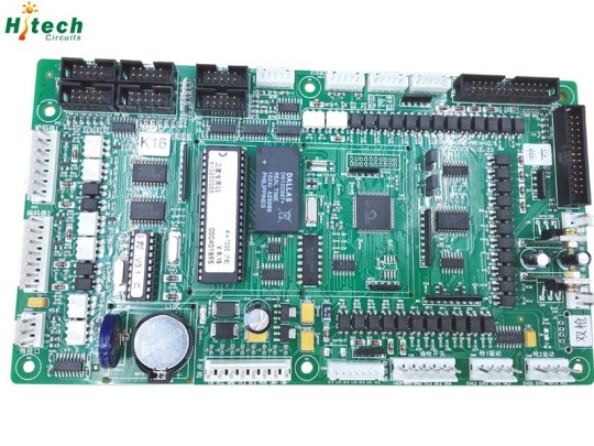
0 notes