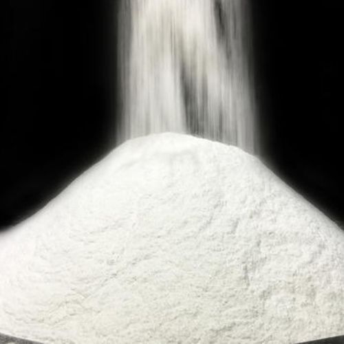
#electronic wet chemicals industry
Explore tagged Tumblr posts
Visit Tumblr Blog
Explore Tumblr blogs with no restrictions, modern design and the best experience.
Last Seen Tumblr Blogs


Fun Fact
The Tumblr office adopted Tommy, an 11-year-old Pomeranian.
Text
Electronic Wet Chemicals Market in Semiconductor Innovation, Trends and Industry Size

The Electronic Wet Chemicals Market has witnessed substantial growth, driven by key factors that have spurred demand and adoption across various industries. The proliferation of electronic devices in consumer electronics, automotive, healthcare, and telecommunications has significantly contributed to this expansion. As these industries progress, there is a parallel need for sophisticated electronic components manufactured with precise wet chemical processes. Technological advancements, particularly in semiconductor and microelectronics manufacturing, have resulted in higher complexity in device architectures and materials, necessitating specialized wet chemicals for intricate processes.
Semiconductor Dominance: Precision in Manufacturing
The dominance of the semiconductor industry as the primary application for electronic wet chemicals is rooted in the indispensable role these substances play in semiconductor manufacturing intricacies. In this sector, where the creation of integrated circuits demands precise and complex processes, wet chemicals emerge as fundamental tools. These chemicals facilitate critical procedures such as etching, cleaning, and material deposition on silicon wafers with unparalleled accuracy, enabling the formation of intricate circuit patterns crucial to semiconductor functionality. Furthermore, the semiconductor realm demands utmost precision and uniformity, achieved through wet chemical processes that ensure consistent treatment across vast manufacturing scales. With a diverse range of semiconductor materials requiring tailored chemical solutions, these substances offer selectivity, allowing precise interactions while safeguarding other materials—a vital aspect in semiconductor patterning and layering. Surface preparation, a pivotal stage in semiconductor production to prevent defects, relies significantly on wet chemicals to meticulously clean and prepare surfaces for subsequent processing steps. Supported by an industry possessing extensive expertise and specialized infrastructure for handling these chemicals, the semiconductor sector's continuous quest for technological advancements further solidifies the critical reliance on electronic wet chemicals in driving innovation and progress within semiconductor manufacturing.
Acetic Acid: Cornerstone of Electronic Wet Chemicals
Acetic acid stands out as a leading type in the electronic wet chemicals market due to its multifaceted utility and compatibility across various critical processes within electronics manufacturing. Its versatility plays a pivotal role, serving diverse functions, including cleaning, etching, and surface preparation, owing to its potent solvent properties adept at efficiently removing contaminants. Moreover, its cost-effectiveness compared to specialized alternatives renders it an economically attractive choice, contributing significantly to its widespread adoption in the industry. In semiconductor manufacturing, acetic acid finds particular favor for its compatibility with crucial processes involved in etching and cleaning semiconductor materials, making it indispensable in the production of integrated circuits and semiconductor devices. The controlled chemical properties of acetic acid, such as its adjustability in acidity and concentration, allow for precise and targeted application throughout various stages of electronic component fabrication. Its relatively safer handling compared to stronger acids further bolsters its preference, balancing effectiveness with safety considerations. With an established history in electronic manufacturing, regulatory compliance, and proven effectiveness, acetic acid remains a stalwart choice, consistently maintaining its dominance as a preferred and widely used type within the electronic wet chemicals market.
Liquid Form Supremacy: Adaptable Solutions for Electronics Manufacturing
The pre-eminence of the liquid form within the electronic wet chemicals market arises from its multifaceted advantages that cater directly to the intricate needs of electronics manufacturing. Liquids offer unparalleled ease of handling and application, boasting fluidity that facilitates precise dispensing, controlled pumping, and meticulous regulation essential for delicate manufacturing processes. Their versatility shines through in their adaptability across a spectrum of applications, from cleaning and etching to deposition and surface treatment, providing solutions to diverse manufacturing needs within the electronics industry. Furthermore, liquids afford a level of precision and uniformity crucial in electronics, ensuring meticulous control over concentration, flow rates, and temperature, thereby safeguarding against variations that could compromise product quality. Compatibility with existing infrastructure is a significant boon, as most electronics manufacturing facilities are tailored to handle liquid chemicals, mitigating the need for extensive modifications. Their efficient heat transfer properties aid in temperature control, safeguarding sensitive electronic components from overheating. Moreover, their safer containment compared to gases and their established industry preference and standardization solidify their dominance as the largest segment in the electronic wet chemicals market, offering a combination of effectiveness, reliability, and adaptability sought after in electronics manufacturing.
Keyplayer of the Electronic Wet Chemicals Market
Key players in this market include Avantor Inc. (US), BASF SE (Germany), Cabot Microelectronics (US), Kanto Chemical Co. Inc. (Japan), Honeywell International, Inc. (US), Eastman Chemical Company (US), Linde Plc (Ireland), Solvay (Belgium), Fujifilm Corporation (Japan), Technic Inc. (US), and more
Request Sample Pages for a detailed insight:
Asia-Pacific: The Epicenter of Electronic Wet Chemicals Market
The Asia-Pacific region stands as the largest market for electronic wet chemicals, primarily driven by several interlinked factors that collectively fuel its dominance in this sector. A pivotal contributor to this status is the region's exponential growth as a global electronics manufacturing hub. Countries such as China, South Korea, Taiwan, and Japan have emerged as major centers for semiconductor fabrication and electronics assembly, consequently propelling substantial demand for electronic wet chemicals across various stages of manufacturing processes. Moreover, the Asia-Pacific region boasts an expanding consumer electronics market, fueled by a burgeoning middle class and increasing disposable income. This surge in demand for devices like smartphones, tablets, televisions, and other electronic gadgets directly correlates to the heightened need for wet chemicals in their production. Additionally, there has been a notable shift of semiconductor production to Asia-Pacific nations, further solidifying the region's pivotal role in driving the electronic wet chemicals market. This strategic relocation aligns with the region's expertise, infrastructural development, and capacity to cater to the soaring demand for semiconductors and electronic components. Collectively, these factors cement the Asia-Pacific region's position as the largest and most influential market for electronic wet chemicals, reflecting its pivotal role in the global electronics manufacturing landscape.
0 notes
Text

Controlling hydrophilicity and hydrophobicity via electron beam-assisted coating technology
Accurate regulation of surface hydrophilicity and hydrophobicity is crucial for various industrial applications, but current methods often lack stability, precision, and scalability. A team of scientists has introduced an electron beam irradiation (EBI)-assisted coating method that provides a reliable and scalable approach to control surface wetting properties. Their work is published in the journal Industrial Chemistry & Materials. "Our study focuses on developing a scalable and reliable solution for controlling hydrophilicity and hydrophobicity of surfaces," says Haozhe Li, the first author from Huazhong University of Science and Technology. "Traditional methods like chemical modification and external stimulation often face challenges such as limited stability and precision, making it difficult to achieve the desired surface properties.
Read more.
13 notes
·
View notes
Text
Comparing Fire Protection Systems: Sprinklers vs. Gas-Based Suppression

Whether a facility is residential, commercial, or industrial, fire prevention is an essential component. Sprinkler systems and gas-based suppression systems are two of the most often used fire control techniques. Both are intended to reduce damage and stop fires from spreading, but they work differently and are appropriate for different types of situations.
To assist you in selecting the best fire safety system for your requirements, we will examine the benefits, drawbacks, and optimal uses of gas-based suppression systems and sprinkler systems in this article.
Understanding Sprinkler Systems

The Operation of Sprinkler Systems
When the heat from a fire exceeds a specific temperature, sprinkler systems—which are water-based fire suppression systems—automatically turn on. Wet pipe systems, the most popular kind, hold water in the pipes so it can be released as needed. Other kinds consist of:
Dry pipe systems are appropriate for cold climates where freezing is a concern since they use pressured air in pipes rather than water.
Pre-action systems: Lower the chance of an unintentional discharge by requiring a two-step procedure prior to activation.
Deluge systems: Made for high-risk locations, these systems instantly unleash a lot of water when they are activated.
Advantages of Sprinkler Systems
Proven Effectiveness: Sprinkler systems are quite successful at containing fires and have been around for more than a century.
Cost-effective: Sprinklers are less expensive to build and maintain than gas-based suppression systems.
Simple Maintenance: Long-term functionality is ensured by routine inspections and small maintenance.
Life Safety: Sprinklers lower the chance of occupant injuries by cooling the surrounding area in addition to putting out flames.
Code Compliance: Sprinkler systems are mandated by numerous building codes across the globe for both residential and commercial buildings.
Limitations of Sprinkler Systems
Water Damage: Sprinklers can seriously harm property and delicate equipment with water damage, notwithstanding their effectiveness.
Restrictions on Applicability: Not recommended for data centers, museums, or locations with expensive or fragile equipment.
Potential Freezing Problems: Pipe water may freeze in cold climates, which could lead to problems.
Understanding Gas-Based Suppression Systems

How Suppression Based on Gas Operates
Gas-based fire suppression systems do not use water to put out fires; instead, they use inert gases or clean agents. These systems function through heat absorption, oxygen displacement, or fire chemical reaction interruption. Typical varieties consist of:
The clean agent FM-200 (HFC-227ea) puts out fires fast and leaves no residue behind.
Although CO2 (carbon dioxide) systems remove oxygen from the fire area, they are dangerous for areas that are occupied.
To safely put out fires in occupied areas, inert gas systems use argon, nitrogen, or a combination of the two.
Novec 1230: An environmentally friendly agent with little effect.
Benefits of Suppression by Gas
Lack of Water Damage: Because gas-based systems don't use water, they safeguard valuable assets, electronics, and delicate equipment.
Fast Activation: These technologies minimize damage and downtime by quickly suppressing fires.
Gas-based fire extinguishers don't leave behind residue, which saves cleanup time in contrast to some chemical extinguishers.
Safe for Sensitive Environments: Perfect for locations where water could seriously harm equipment, such as server rooms, archives, museums, data centers, and pharmaceutical labs.
Gas-Based Suppression's Drawbacks
Greater Cost: Compared to sprinklers, installation and upkeep are more costly.
Sealed Environment Needed: To keep gas from escaping, these devices work best in rooms that are tightly sealed.
Possible Safety Risks: If not correctly handled, certain gases, such as CO₂, might be dangerous to individuals in enclosed places.
Recharging After Discharge: Gas-based systems need to have costly gas agents replaced, in contrast to sprinklers, which may be refilled with water.
Choosing the Right System for Your Needs
Take into account the following elements while choosing a fire suppression system:
Nature of Assets and Equipment: A gas-based system is a preferable choice if your area has delicate equipment (such as a server room). Sprinkler systems for general-purpose spaces are dependable and reasonably priced.
Budget: While gas-based systems demand a bigger initial investment yet provide better protection for valuable goods, sprinklers are less expensive up front.
Regulatory Requirements: Depending on the type of structure and its intended use, your region's fire rules may require a particular suppression system.
Potential for Water Damage: A gas-based system is a safer option if exposure to water could destroy inventory or equipment.
Occupant Safety: Gas-based systems need to be carefully planned in occupied places to avoid exposure to specific gases, even if both systems are made to be safe.
Final Thoughts
Effective fire protection is provided by both gas-based and sprinkler-based fire suppression systems; however, the decision is based on the particular requirements of the building and its contents. Gas-based suppression systems offer specific protection for locations where water damage is a significant issue, whereas sprinkler systems are frequently employed because of their affordability and track record of dependability.
To ensure you have the proper fire protection in place, work with the best fire and safety company in Saudi Arabia, such as Axontec International, which can inspect your building and recommend the most suitable fire suppression system. Investing in the right system guarantees business continuity, employee and asset safety, and property protection.
0 notes
Text
Rheology Modifier for Adhesives Market, Global Outlook and Forecast 2025-2032
Rheology modifiers for adhesives are specialized additives designed to control the viscosity, flow, and consistency of adhesive formulations. These modifiers improve application properties such as sag resistance, tack, and wetting, ensuring optimal performance in various industrial and commercial applications. Rheology modifiers encompass thickeners, flow control agents, and viscosity stabilizers, playing a critical role in enhancing the efficiency and reliability of adhesives used in construction, automotive, packaging, and other sectors.
Market Size
Download FREE Sample of this Report @ https://www.24chemicalresearch.com/download-sample/286633/global-rheology-modifier-for-adhesives-forecast-market-2025-2032-940
The global Rheology Modifier for Adhesives market was valued at USD 574 million in 2023 and is expected to reach USD 705.95 million by 2032, growing at a compound annual growth rate (CAGR) of 3.00%. This steady market expansion is driven by the increasing demand for high-performance adhesives across multiple industries, as well as advancements in rheology modifier formulations that enhance product performance.
North America remains a significant market, with a valuation of USD 149.57 million in 2023. The region is projected to grow at a CAGR of 2.57% from 2025 through 2032, supported by strong demand in the automotive and construction industries. Europe and Asia-Pacific also present substantial growth opportunities, with expanding industrial applications and rising investments in adhesive technologies.
Market Dynamics (Drivers, Restraints, Opportunities, and Challenges)
Drivers
Growing Demand for High-Performance Adhesives: Industries such as construction, automotive, and packaging increasingly rely on adhesives with superior performance characteristics, driving the need for effective rheology modifiers.
Technological Advancements: Continuous innovation in polymer science and material engineering is enhancing the efficiency and sustainability of rheology modifiers, fueling market growth.
Expansion of End-Use Industries: The rising adoption of adhesives in new applications, including medical devices and electronics, is boosting demand for tailored rheology modification solutions.
Restraints
High Cost of Specialty Additives: The development and production of advanced rheology modifiers involve significant R&D and manufacturing costs, which may limit adoption in price-sensitive markets.
Regulatory Challenges: Stringent environmental and safety regulations regarding chemical formulations can pose compliance challenges for manufacturers.
Opportunities
Sustainability Trends: Increasing demand for eco-friendly and biodegradable adhesives opens new avenues for the development of green rheology modifiers.
Growth in Emerging Markets: Rapid industrialization in regions such as Asia-Pacific and Latin America presents significant expansion opportunities for rheology modifier manufacturers.
Challenges
Supply Chain Disruptions: Fluctuations in raw material availability and logistics constraints can impact production and pricing.
Competition from Alternative Technologies: The rise of novel adhesive formulations with inherent rheological stability may reduce dependency on traditional rheology modifiers.
Regional Analysis
North America
North America holds a strong position in the rheology modifiers market due to established industrial sectors, technological advancements, and a focus on sustainable adhesive solutions.
Europe
Europe’s stringent environmental regulations and demand for high-performance adhesives drive market growth, with key players focusing on innovative and sustainable product development.
Asia-Pacific
The Asia-Pacific region is expected to witness the highest growth rate due to rapid industrial expansion, increased construction activities, and rising automotive production.
Middle East & Africa
Growing infrastructure projects and an increasing focus on advanced adhesive applications contribute to market development in this region.
Competitor Analysis (In Brief)
Key players in the Rheology Modifier for Adhesives market include:
BASF SE – A leader in chemical manufacturing, offering advanced rheology modifier solutions.
Dow Inc. – Focuses on high-performance and sustainable adhesive formulations.
Clariant AG – Develops specialty additives for adhesives and coatings.
Elementis PLC – Specializes in rheology modification for industrial applications.
Arkema S.A. – Provides innovative polymer solutions to enhance adhesive performance.
These companies compete on factors such as innovation, product quality, sustainability, and customer relationships.
Global Rheology Modifier for Adhesives Market Segmentation Analysis
This report provides a deep insight into the global Rheology Modifier for Adhesives market, covering all its essential aspects. This ranges from a macro overview of the market to micro details of the market size, competitive landscape, development trend, niche market, key market drivers and challenges, SWOT analysis, value chain analysis, etc.
The analysis helps the reader to shape the competition within the industries and strategies for the competitive environment to enhance potential profit. Furthermore, it provides a simple framework for evaluating and assessing the position of the business organization. The report structure also focuses on the competitive landscape of the Global Rheology Modifier for Adhesives market. This report introduces in detail the market share, market performance, product situation, operation situation, etc., of the main players, which helps the readers in the industry to identify the main competitors and deeply understand the competition pattern of the market.
In a word, this report is a must-read for industry players, investors, researchers, consultants, business strategists, and all those who have any kind of stake or are planning to foray into the Rheology Modifier for Adhesives market in any manner.
Market Segmentation (by Application)
Construction Adhesives
Automotive Adhesives
Packaging Adhesives
Electronics Adhesives
Medical Adhesives
Others
Construction Adhesives
Automotive Adhesives
Packaging Adhesives
Electronics Adhesives
Medical Adhesives
Others
Market Segmentation (by Type)
Organic Rheology Modifiers
Inorganic Rheology Modifiers
Organic Rheology Modifiers
Inorganic Rheology Modifiers
Key Company
BASF SE
Dow Inc.
Clariant AG
Elementis PLC
Arkema S.A.
BASF SE
Dow Inc.
Clariant AG
Elementis PLC
Arkema S.A.
Geographic Segmentation
North America
Europe
Asia-Pacific
Middle East & Africa
Latin America
North America
Europe
Asia-Pacific
Middle East & Africa
Latin America
FAQ Section
What is the current market size of the Rheology Modifier for Adhesives market?
The global market was valued at USD 574 million in 2023 and is projected to reach USD 705.95 million by 2032, growing at a CAGR of 3.00%.
Which are the key companies operating in the Rheology Modifier for Adhesives market?
Major players include BASF SE, Dow Inc., Clariant AG, Elementis PLC, and Arkema S.A.
What are the key growth drivers in the Rheology Modifier for Adhesives market?
Key drivers include the increasing demand for high-performance adhesives, technological advancements, and expansion in end-use industries.
Which regions dominate the Rheology Modifier for Adhesives market?
North America, Europe, and Asia-Pacific are the leading regions, with significant growth in the U.S., China, and Germany.
What are the emerging trends in the Rheology Modifier for Adhesives market?
Emerging trends include the development of eco-friendly rheology modifiers, increased investment in adhesive innovation, and advancements in polymer chemistry.
Get the Complete Report & TOC @ https://www.24chemicalresearch.com/reports/286633/global-rheology-modifier-for-adhesives-forecast-market-2025-2032-940 Table of content
Table of Contents 1 Research Methodology and Statistical Scope 1.1 Market Definition and Statistical Scope of Rheology Modifier for Adhesives 1.2 Key Market Segments 1.2.1 Rheology Modifier for Adhesives Segment by Type 1.2.2 Rheology Modifier for Adhesives Segment by Application 1.3 Methodology & Sources of Information 1.3.1 Research Methodology 1.3.2 Research Process 1.3.3 Market Breakdown and Data Triangulation 1.3.4 Base Year 1.3.5 Report Assumptions & Caveats 2 Rheology Modifier for Adhesives Market Overview 2.1 Global Market Overview 2.1.1 Global Rheology Modifier for Adhesives Market Size (M USD) Estimates and Forecasts (2019-2032) 2.1.2 Global Rheology Modifier for Adhesives Sales Estimates and Forecasts (2019-2032) 2.2 Market Segment Executive Summary 2.3 Global Market Size by Region 3 Rheology Modifier for Adhesives Market Competitive Landscape 3.1 Global Rheology Modifier for Adhesives Sales by Manufacturers (2019-2025) 3.2 Global Rheology Modifier for Adhesives Revenue Market Share by Manufacturers (2019-2025) 3.3 Rheology Modifier for Adhesives Market Share by Company Type (Tier 1, Tier 2, and Tier 3) 3.4 Global Rheology Modifier for Adhesives Average Price by Manufacturers (2019-2025) 3.5 Manufacturers Rheology Modifier for Adhesives Sales Sites, Area Served, Product Type 3.6 Rheology Modifier for Adhesives Market Competitive Situation and Trends 3.6.1 Rheology Modifier for Adhesives Market Concentration Rate 3.6.2 Global 5 and 10 Largest Rheology Modifier for ACONTACT US: North Main Road Koregaon Park, Pune, India - 411001. International: +1(646)-781-7170 Asia: +91 9169162030
Follow Us On linkedin :- https://www.linkedin.com/company/24chemicalresearch/
0 notes
Text
Semiconductor Abatement Systems Market Report 2024-2032 by Reports and Insights

The Reports and Insights, a leading market research company, has recently releases report titled “Semiconductor Abatement Systems Market: Global Industry Trends, Share, Size, Growth, Opportunity and Forecast 2024-2032.” The study provides a detailed analysis of the industry, including the global Semiconductor Abatement Systems Market share, size, trends, and growth forecasts. The report also includes competitor and regional analysis and highlights the latest advancements in the market.
Report Highlights:
How big is the Semiconductor Abatement Systems Market?
The global semiconductor abatement systems market size reached US$ 800.7 million in 2023. Looking forward, Reports and Insights expects the market to reach US$ 1,998.9 million in 2032, exhibiting a growth rate (CAGR) of 10.7% during 2024-2032.
What are Semiconductor Abatement Systems?
Semiconductor abatement systems are advanced tools used in the semiconductor manufacturing process to remove hazardous gases and chemicals. These systems play a critical role in maintaining a safe and clean working environment by efficiently neutralizing and treating exhaust gases and process by-products. Semiconductor abatement systems are essential for controlling emissions and ensuring compliance with environmental regulations in semiconductor fabrication facilities. They are designed to handle a wide range of toxic gases, including fluorine, chlorine, and arsine, providing a reliable and efficient solution for managing waste gases in semiconductor manufacturing.
Request for a sample copy with detail analysis: https://www.reportsandinsights.com/sample-request/1856
What are the growth prospects and trends in the Semiconductor Abatement Systems industry?
The semiconductor abatement systems market growth is driven by various and trends. The market for semiconductor abatement systems is a critical component of the semiconductor industry, fueled by the rising need for advanced manufacturing processes and strict environmental guidelines. These systems play a vital role in eliminating hazardous gases and chemicals used in semiconductor manufacturing, ensuring both a safe workplace and adherence to regulatory standards. Market growth is driven by factors like increased adoption of abatement systems in semiconductor fabrication plants, a growing emphasis on sustainability, and the demand for effective solutions for managing waste gases. Furthermore, ongoing technological advancements, including the creation of more efficient and economical abatement systems, are driving the market's expansion. Hence, all these factors contribute to semiconductor abatement systems market growth.
What is included in market segmentation?
The report has segmented the market into the following categories:
By Type:
Wet Abatement Systems
Dry Abatement Systems
By Process:
Etch Abatement Systems
Chemical Vapor Deposition (CVD) Abatement Systems
Physical Vapor Deposition (PVD) Abatement Systems
Chemical Mechanical Planarization (CMP) Abatement Systems
Others
By End-Use:
Semiconductor Manufacturers
Foundries
Packaging and Assembly Service Providers
Others
By Application:
Logic and Memory Devices
Micro-electromechanical Systems (MEMS)
Power Devices
Optoelectronics
Others
By Sales Channel:
Direct Sales
Distributor Sales
Market Segmentation By Region:
North America
United States
Canada
Europe
Germany
United Kingdom
France
Italy
Spain
Rest of Europe
Asia Pacific
China
Japan
India
South Korea
Rest of Asia Pacific
Latin America
Brazil
Mexico
Argentina
Middle East & Africa
Saudi Arabia
South Africa
United Arab Emirates
Israel
Who are the key players operating in the industry?
The report covers the major market players including:
Applied Materials Inc.
Lam Research Corporation
Tokyo Electron Limited
Hitachi High-Technologies Corporation
Axcelis Technologies Inc.
Edwards Vacuum LLC
Aeronex Inc.
DAS Environmental Expert GmbH
MKS Instruments Inc.
AMEC International Limited
TEL NEXX, Inc.
Ultra Clean Holdings, Inc.
CVD Equipment Corporation
View Full Report: https://www.reportsandinsights.com/report/Semiconductor Abatement Systems-market
If you require any specific information that is not covered currently within the scope of the report, we will provide the same as a part of the customization.
About Us:
Reports and Insights consistently mееt international benchmarks in the market research industry and maintain a kееn focus on providing only the highest quality of reports and analysis outlooks across markets, industries, domains, sectors, and verticals. We have bееn catering to varying market nееds and do not compromise on quality and research efforts in our objective to deliver only the very best to our clients globally.
Our offerings include comprehensive market intelligence in the form of research reports, production cost reports, feasibility studies, and consulting services. Our team, which includes experienced researchers and analysts from various industries, is dedicated to providing high-quality data and insights to our clientele, ranging from small and medium businesses to Fortune 1000 corporations.
Contact Us:
Reports and Insights Business Research Pvt. Ltd. 1820 Avenue M, Brooklyn, NY, 11230, United States Contact No: +1-(347)-748-1518 Email: [email protected] Website: https://www.reportsandinsights.com/ Follow us on LinkedIn: https://www.linkedin.com/company/report-and-insights/ Follow us on twitter: https://twitter.com/ReportsandInsi1
#Semiconductor Abatement Systems Market share#Semiconductor Abatement Systems Market size#Semiconductor Abatement Systems Market trends
0 notes
Text
Top-Quality FEP Wires for Durability
At The Tanya Enterprises, we deal in quality FEP wires with resistance to different weather conditions, durability, and thermal insulation. These wires use Fluorinated Ethylene Propylene (FEP) as insulation, a high-performance material known for excellent heat, chemical, and moisture resistance.
What Are FEP Wires?
FEP wires are electric wires having fluoroethylene propylene as insulation of varying densities. These wires are very flexible and thus very useful in environmental conditions that can be highly demanding across various industries. They exhibit excellent nonstick properties with very high dielectric strength and high thermal resistance.

Benefits of FEP Wires
High-Temperature Resistance: It can withhold temperatures not exceeding 200 degrees centigrade, making it suitable for harsh applications.
Chemicals Resistance: Useful in very aggressive chemical environments since they can resist damage from oils and solvents.
Non-wetting Ability: These wires do not wet and are not easily dammed, which makes such types ideally suited for humid and extremely soggy conditions.
Excellent Flexibility: Makes them easy to install, curve, and use for complex wiring installations.
Non-combustible: The wires are considered quite safe, due to the nature of FEP being flame resistant.
Uses Of FEP Wires
The FEP wires are used in the industries.
Electronic and electrical apparatus – In electrical circuits, control, and other devices.
The automotive industry – In automotive wiring, FEP is chosen due to heat and chemical resistance.
Medical devices – Used in medical devices that require wiring that is durable and sterile.
Aerospace – FEP wires have become indispensable with their reliability as assets of wiring circuits.
Why Tanya Enterprises?
At Tanya Enterprises, we firmly stand for nothing less than international standards in the quality of our products. Our FEP wires go through detailed testing to guarantee excellent performance and durability. Competitive pricing, timely delivery, and best-in-class support.
Visit - https://www.insulatedwires.com/ Address- Factory 46-Vedvyaspuri Industrial Area, Sector-8 Meerut Pin-250103, INDIA
1 note
·
View note
Text
Near-infrared Spectroscopy Market: A Comprehensive Overview of Growth and Innovation
The global near-infrared spectroscopy market size is expected to reach USD 806.4 million by 2030, registering a CAGR of 5.8% over the forecast period, according to a new report by Grand View Research, Inc. The growing implementation of an analytical technique for raw materials in numerous sectors, such as oil & gas and agriculture, coupled with their increasing applications is anticipated to spur industry growth. For instance, various herbs and plants with therapeutic and medicinal properties are analyzed through near-infrared (NIR) spectroscopy to assess the bio-active components. The industry has witnessed considerable growth in 2021 and is expected to have similar developments during the forecasted period.
The demand for the products from the material science sector is a substantial contributor to the revenue. NIR spectrometry provides significant advantages as a process analytical technology over other techniques including wet chemical methods, resulting in increasing preference from manufacturers. Other determinants, such as rapid advancement in the workflows of material verification, as well as improving risk management in the supply chain by manufacturers to fulfill the GMP criteria, are also contributing to the growth. The major 20 pharmaceutical manufacturers employ portable NIR analyzers to authenticate either raw materials or finished products to comply with GMP guidelines. Similarly, regulatory bodies in Europe, North America, Africa, and Asia have purchased the product to strengthen their counterfeiting efforts.
The COVID-19 pandemic had a positive impact on the demand from pharmaceutical manufacturers. However, the disruptions in industries, such as electronics & semiconductors, food & beverages, and chemical, are projected to have an adverse impact on the growth rate. For instance, in February 2021, the U.S. government reviewed the supply chain of pharma and semiconductors to strengthen the domestic investment and process of manufacturing. The imposed lockdown norms across the globe created shortages in supplies and inflated the cost of raw materials, this affected the profitability of the players. Similarly, the capability of NIR spectroscopy to identify the polymers that are used in the packaging of pharmaceutical and nutraceutical products is anticipated to be another determinant of industry growth.
Gather more insights about the market drivers, restrains and growth of the Near-infrared Spectroscopy Market
Near-infrared Spectroscopy Market Report Highlights
• The Fourier Transform-based (FT-NIR) spectrometers product segment held the major revenue share owing to the high accuracy in the material testing and verification
• The particle measurement application segment had a substantial share in 2022 due to strict measures by emerging countries for dealing with counterfeited medicines
• The portable near-infrared spectroscopy type segment is anticipated to register the fastest CAGR during the forecasted period
• MicroPHAZIR RX analyzer by Thermo Fisher Scientific is one of the portable NIR spectrometry that can analyze various applications
• Europe dominated the global industry in 2022 due to the establishment of a large number of pharmaceutical manufacturers and strict regulations for quality-check as a part of GMP compliance
• Asia Pacific is estimated to grow at the fastest CAGR over the forecasted period owing to the expansion of the semiconductors industry in emerging regions, such as India
Near-infrared Spectroscopy Market Segmentation
Grand View Research has segmented the global near-infrared Spectroscopy market based on product, type, application, and region:
NIR Spectroscopy Product Outlook (Revenue, USD Million, 2018 - 2030)
• Dispersive Infrared Spectroscopy
• Fourier Transform-Based (FT-NIR) Spectrometers
NIR Spectroscopy Type Outlook (Revenue, USD Million, 2018 - 2030)
• Benchtop
• Portable
NIR Spectroscopy Application Outlook (Revenue, USD Million, 2018 - 2030)
• Medical Applications
• Astronomical Spectroscopy
• Remote Monitoring
• Agriculture
• Particle Measurement
• Material Science
• Industrial Use
NIR Spectroscopy Regional Outlook (Revenue, USD Million, 2018 - 2030)
• North America
o U.S.
o Canada
• Europe
o U.K.
o Germany
o France
o Italy
o Spain
• Asia Pacific
o Japan
o China
o India
o South Korea
o Australia
• Latin America
o Brazil
o Mexico
o Argentina
• Middle East & Africa
o South Africa
o Saudi Arabia
o UAE
Order a free sample PDF of the Near-infrared Spectroscopy Market Intelligence Study, published by Grand View Research.
#Near-infrared Spectroscopy Market#Near-infrared Spectroscopy Market Size#Near-infrared Spectroscopy Market Share#Near-infrared Spectroscopy Market Analysis#Near-infrared Spectroscopy Market Growth
0 notes
Text
Why Is Glass Epoxy Ideal for Tile Joints and What Is It?
Glass epoxy is a revolutionary material for producing seamless, long-lasting, and aesthetically pleasing tile coatings. Glass epoxy for tiles has been a popular option for both professionals and homeowners for a variety of applications, including commercial spaces, industrial flooring, and bathrooms. What is glass epoxy, though, and why should you use it for your upcoming tile project? Let's take a closer look.
Glass Epoxy: What is it?
Glass epoxy is a specialty filler and glue that blends hardener and resin to produce a durable, glossy finish. It is frequently utilized in many different applications, such as electronics, ornamental objects, and—above all—as a filler for tile joints. Glass epoxy is perfect for wall and floor tiles because it offers a surface that is smooth, watertight, and stain-resistant.
Glass Epoxy's Advantages for Tile Joints
Glass epoxy is a better option than conventional grout or cement-based fillers for tiles since it provides a number of unparalleled advantages. Here are a few main benefits:
1. Smooth Finish
Glass epoxy produces a flawless, smooth surface that improves tiled areas' visual appeal. Any space is made more sophisticated by its shiny finish.
2. Superior Sturdiness
Epoxy fillers for tile joints are renowned for their extraordinary durability and strength. They are ideal for commercial and industrial flooring because they can tolerate high foot activity.
3. Stain-resistant and waterproof
Glass epoxy is completely watertight, in contrast to regular grout. This makes it perfect for places like restrooms, kitchens, and swimming pools that are subjected to water. It is also easy to clean and stain-resistant.
4. Resistance to Chemicals
Due to its chemical resistance, glass epoxy can be used in industrial settings where spills and contact with harsh materials are frequent occurrences.
5. Lifespan
After application, glass epoxy can endure for years without requiring regular upkeep, making it an affordable option over time.
An Innovative Approach to Tile Adhesion: Glass Bond Epoxy
Glass bond epoxy is an additional notable choice when selecting an adhesive or filler for tiles. This kind of epoxy helps to stabilize the wall or flooring overall in addition to guaranteeing a solid tile-to-tile adhesion. Because of its superior adhesive qualities, it can be used for intricate tile jobs where durability and accuracy are crucial.
Epoxy applications for floor tiles
Glass epoxy is essential for maintaining the durability of floor tiles and isn't just for joint filling. Typical uses include the following:
Residential flooring: Epoxy for floor tiles improves the look and longevity of tiled flooring in living areas and kitchens.
Commercial Spaces: Epoxy's robust floor tile performance is advantageous for shopping centers, workplaces, and retail establishments.
Industrial Flooring: Glass epoxy is ideal for industries and warehouses because to its resilience to chemicals and large machinery.
Wet Areas: Glass epoxy is essential for waterproofing bathrooms, swimming pools, and spas.
How Epoxy Tile Joint Filler Is Applied
It takes skill and accuracy to apply glass epoxy to tile joints. Here is a basic guide:
Surface Preparation: Make sure the seams and tiles are dry and clean.
Mix the Epoxy: As directed by the manufacturer, mix the resin and hardener.
Apply the Epoxy: Fill the joints uniformly using a spatula or applicator.
Smooth the Surface: For a consistent finish, remove extra epoxy and smooth out the joints.
Cure the Epoxy: Give the epoxy time to fully cure, usually 24 to 48 hours.
Durofill Glass Epoxy: Why Choose It?
Our specialty at Durofill is offering premium glass epoxy for tiles that satisfies the strictest industry requirements. Whether you're working on commercial, industrial, or residential projects, our products are made to function exceptionally well. Durofill glass epoxy is the best choice for your tiling requirements because of its emphasis on strength, visual attractiveness, and simplicity of use.
Final thoughts
Glass epoxy is more than just a filler or glue; it's a long-term investment in the appearance and functionality of your tiled spaces. Epoxy tile joint filler and adhesives offer unparalleled benefits, whether you're looking for a smooth surface, waterproofing, or durability. Choose Durofill for all of your glass epoxy requirements to observe the improvement in quality and performance.
Conclusion
Using glass epoxy in your tiling projects guarantees longevity, style, and ease of upkeep. Glass epoxy for tiles is essential for getting results that are on par with those seen in commercial floors and private bathrooms. Durofill is committed to offering precise, high-quality solutions that satisfy your needs. Our products are made to last, whether they are epoxy for floor tiles or glass bond epoxy. Enjoy the unique combination of elegance and utility that glass epoxy offers by transforming your environments with its unparalleled benefits today!
#epoxy tile joint filler#glass bond epoxy#glass epoxy#benefits of glass epoxy#epoxy for floor tiles#glass epoxy for tiles#what is glass epoxy
0 notes
Text
The key material for sintering nitride ceramic substrates - Boron Nitride Crucible
Nitride ceramics have refractory compounds of nitrogen and metal or non-metal elements covalently bonded as the main component. The most widely used ceramics include silicon nitride (Si3N4), aluminum nitride (AlN), boron nitride (BN), and other ceramics. Among them, due to their excellent hardness, mechanical strength and heat dissipation, silicon nitride ceramics, and aluminum nitride ceramics can be made into ceramic substrates for electronic packaging, which have good development prospects. In the preparation process of aluminum nitride and silicon nitride ceramic substrates, boron nitride ceramics play an important role.

Cubic boron nitride and hexagonal boron nitride are relatively common crystal forms. Cubic boron nitride has a structure similar to diamond, is extremely hard, and is widely used in industrial drilling and grinding tools. Hexagonal boron nitride (hexagonal boron nitride) is a white powder and an advanced ceramic material. Its crystal structure is very similar to that of graphite, and the physical and chemical properties of the two are also identical. Therefore, hexagonal boron nitride is also called "white graphite" and is the most commonly used form of boron nitride.
Characteristics of hexagonal boron nitride:
-The expansion coefficient is equivalent to quartz, but the thermal conductivity is ten times that of quartz, which is the same as stainless steel. The high thermal conductivity of hot-pressed products is 33W/mK, and the thermal shock resistance is excellent;
-In terms of mechanical properties, it has the advantages of non-abrasiveness, good lubricity, and easy processing;
-In terms of electrical properties, it has the advantages of good dielectric strength, low dielectric constant, low loss at high frequency, microwave penetration, and good electrical insulation;
-In terms of thermal properties, it has the advantages of high thermal conductivity, high heat capacity, low thermal expansion, thermal shock resistance, high-temperature lubricity and high-temperature safety;
-In terms of chemical properties, it has the advantages of chemical stability, corrosion resistance, oxidation resistance, low wetting, biological stability, and non-stick properties.
Sintering crucible for silicon nitride/aluminum nitride substrate
A boron nitride crucible can be used for sintering silicon nitride substrate/structural parts, aluminum nitride substrate/structural parts, etc. The maximum operating temperature is 2100℃ (in inert atmosphere). It has the characteristics of high and low-temperature repeated impact resistance, corrosion resistance, no reaction with metal and ceramic materials, no adhesion, long service life, etc. It can replace graphite and alumina crucibles.
Edgetech is a professional ceramic supplier, we have many years of experience in producing high-quality precision ceramic parts. We use our experienced team and in-depth understanding of ceramic materials to create the best precision ceramic products for our customers at very competitive prices.
0 notes
Text
A Comprehensive Guide to Hydrogen Sulphide Testing Methods
Hydrogen sulphide (H₂S) is a colorless gas with a distinct rotten egg smell, commonly found in industrial processes, wastewater systems, and natural gas production. Due to its toxic nature and potential to cause serious health and environmental risks, conducting a reliable Hydrogen Sulphide test is essential for safety and compliance. This guide explores various testing methods and their applications.

What is Hydrogen Sulphide?
Hydrogen sulphide is a naturally occurring gas often produced by the breakdown of organic matter in anaerobic conditions. It is highly toxic, flammable, and corrosive, making it critical to detect and monitor its presence in various environments, including:
Industrial facilities
Wastewater treatment plants
Natural gas extraction sites
Agricultural settings
Why Conduct a Hydrogen Sulphide Test?
Testing for hydrogen sulphide is vital for several reasons:
Health and Safety: Prolonged exposure to H₂S can lead to serious health problems, including respiratory issues, eye irritation, and in high concentrations, it can be fatal.
Environmental Protection: H₂S contributes to air pollution and poses risks to water systems.
Compliance: Industries must adhere to environmental and occupational safety regulations, which often require regular monitoring of H₂S levels.
Common Hydrogen Sulphide Testing Methods
Gas Detection Tubes
Gas detection tubes are one of the simplest methods for measuring hydrogen sulphide levels. They contain a chemical reagent that changes color when exposed to H₂S.
Advantages:
Portable and easy to use
Cost-effective for quick, on-site testing
Limitations:
Limited accuracy and sensitivity
Not suitable for continuous monitoring
Electronic Gas Detectors
Electronic detectors are widely used for detecting H₂S in industrial settings. These devices use sensors, such as electrochemical or infrared, to measure gas concentration.
Advantages:
High accuracy and sensitivity
Real-time monitoring
Can be integrated into safety systems
Limitations:
Higher initial cost
Requires regular calibration and maintenance
Wet Chemical Methods
These methods involve using chemical reagents to react with H₂S and quantify its concentration. Examples include the iodometric and methylene blue methods.
Advantages:
Suitable for laboratory analysis
Provides detailed results
Limitations:
Time-consuming
Requires specialized equipment and expertise
Optical Methods
Optical techniques, such as UV-Vis spectroscopy, detect H₂S by measuring the absorbance of light at specific wavelengths.
Advantages:
High precision
Can detect low concentrations
Limitations:
Expensive equipment
Requires a controlled environment
Colorimetric Test Kits
These kits use color change to indicate the presence of H₂S. They are often used for water testing.
Advantages:
Simple and user-friendly
Suitable for field applications
Limitations:
Limited accuracy
May not detect very low concentrations
Choosing the Right Method
The choice of a Hydrogen Sulphide test depends on several factors:
Application: Is the test for air, water, or soil? Different methods are better suited for specific environments.
Required Sensitivity: Determine the detection limits necessary for your application.
Cost and Resources: Consider the budget and available equipment.
Frequency of Testing: Choose a method that aligns with the need for periodic or continuous monitoring.
Best Practices for Hydrogen Sulphide Testing
Regular Calibration: Ensure testing equipment is calibrated for accurate readings.
Follow Manufacturer Guidelines: Adhere to instructions for test kits and equipment.
Use Protective Gear: H₂S is hazardous; always use appropriate safety equipment.
Engage Professionals: For complex testing needs, consult certified labs or specialists.
Conclusion
Conducting a reliable Hydrogen Sulphide test is crucial for ensuring safety, environmental protection, and regulatory compliance. By understanding the various testing methods and their applications, you can select the most suitable approach for your needs. Whether it’s a quick field test or a detailed laboratory analysis, prioritizing regular H₂S testing helps mitigate risks and promotes a safer environment.
For expert hydrogen sulphide testing services, reach out to CoreLab.org and ensure your workplace or facility remains compliant and safe.
0 notes
Text
Top 15 Market Players in Global Powder Coating Additives Market

Top 15 Market Players in Global Powder Coating Additives Market
The powder coating additives market is experiencing rapid growth, driven by increased demand for durable, eco-friendly coatings across industries such as automotive, construction, and electronics. Below are the 15 leading companies shaping the global powder coating additives market:
AkzoNobel N.V. A leader in coatings and chemicals, AkzoNobel provides a wide range of powder coating additives for superior surface finishes and performance.
Axalta Coating Systems Axalta focuses on innovative coating solutions, offering advanced additives that enhance adhesion, flow, and durability in powder coatings.
BASF SE BASF is a major player in the chemical industry, supplying high-performance powder coating additives designed for various industrial applications.
The Sherwin-Williams Company Sherwin-Williams offers a broad portfolio of powder coating additives that improve aesthetics, corrosion resistance, and UV protection.
PPG Industries, Inc. PPG provides powder coating additives with excellent properties, including leveling, gloss control, and surface hardness.
Evonik Industries AG A leader in specialty chemicals, Evonik develops powder coating additives that improve flow, dispersion, and surface finish.
Clariant AG Clariant produces innovative additives for powder coatings, focusing on sustainability and enhanced performance.
Arkema Group Arkema offers advanced resin and additive technologies for powder coatings, emphasizing durability and eco-friendliness.
Eastman Chemical Company Eastman supplies powder coating additives that enhance adhesion, flexibility, and overall coating performance.
King Industries, Inc. King Industries develops specialty additives for powder coatings, including flow modifiers and curing agents.
BYK-Chemie GmbH BYK provides a comprehensive range of additives, including wetting, leveling, and surface improvement solutions for powder coatings.
Allnex Known for its advanced resins and additives, Allnex delivers powder coating additives for industrial and decorative applications.
Lubrizol Corporation Lubrizol focuses on high-performance additives that enhance durability, gloss retention, and chemical resistance in powder coatings.
Troy Corporation Troy supplies specialty additives, including anti-microbial and anti-corrosion solutions for powder coatings.
Perstorp Holding AB Perstorp offers powder coating additives that provide enhanced cross-linking, adhesion, and environmental sustainability.
Request report sample at https://datavagyanik.com/reports/global-powder-coating-additives-market/
Top Winning Strategies in Powder Coating Additives Market
To remain competitive and capitalize on growth opportunities, companies in the powder coating additives market are employing the following strategies:
Focus on Sustainability Companies are prioritizing eco-friendly additives to align with global environmental regulations and meet consumer demand for green solutions.
Investment in R&D Continuous innovation to develop additives with enhanced performance, durability, and aesthetic properties is a key focus for market players.
Customization of Products Tailoring additives to meet specific customer requirements, such as gloss control or abrasion resistance, helps companies differentiate their offerings.
Expanding into Emerging Markets Targeting high-growth regions, particularly in Asia-Pacific and Latin America, provides opportunities to tap into growing industrialization and construction activities.
Strategic Partnerships Collaborations with coating manufacturers enable the development of integrated solutions and increase market reach.
Enhancing Product Portfolios Expanding additive offerings to include multifunctional solutions, such as those that combine anti-corrosion and UV resistance, adds value for customers.
Digital Marketing and Awareness Campaigns Educating end-users about the benefits of advanced powder coating additives through webinars, trade shows, and digital platforms boosts adoption.
Adoption of Bio-Based Additives Incorporating bio-based and renewable raw materials into additive formulations addresses the growing demand for sustainable solutions.
Mergers and Acquisitions Acquiring smaller companies or startups with innovative technologies allows major players to expand their capabilities and market presence.
Geographic Diversification Establishing production facilities and distribution networks in new regions reduces dependency on specific markets and ensures supply chain resilience.
Focus on Regulatory Compliance Ensuring products meet stringent safety and environmental standards enhances credibility and facilitates market expansion.
Cost Optimization Streamlining production processes and optimizing raw material sourcing enable companies to offer competitive pricing without compromising quality.
Integration of Advanced Technologies Leveraging technologies like nanotechnology and AI-driven formulation design allows for the development of next-generation powder coating additives.
Improving Supply Chain Efficiency Strengthening logistics and distribution channels ensures timely delivery of products and improves customer satisfaction.
Targeting High-Growth Applications Expanding additive usage in industries like automotive, consumer electronics, and renewable energy broadens revenue opportunities.
By implementing these strategies, market players can strengthen their position, drive innovation, and capitalize on the increasing demand for powder coating additives across various industries.
Request a free sample copy at https://datavagyanik.com/reports/global-powder-coating-additives-market/
#Powder Coating Additives Market#Powder Coating Additives Production#market players#market share#revenue#top trends#market size#average price
0 notes
Text
How Do Waste Water Treatment Companies in UAE Contribute to Sustainability?
The United Arab Emirates (UAE) is a leader in modern development, constantly working to ensure a balance between growth and environmental protection. With limited natural water resources and a growing population, managing water sustainably is crucial for the UAE. One way the country tackles this challenge is through waste water treatment companies, which help recycle and reuse water while reducing environmental harm.
Among these companies, Water Engineering Technologies (WET FZC) is a key player, offering innovative solutions to ensure clean and safe water for various industries and communities. This blog will explain how such companies contribute to sustainability and how they help secure water resources for the future.
Why Sustainability is Important for Water in UAE
The UAE is a desert nation where fresh water is scarce. Most of the water supply comes from energy-intensive desalination or ground reserves that are depleting quickly. Meanwhile, urbanization and industrialization are increasing the demand for water, making efficient water management critical.
Key Challenges:
Scarcity of natural water resources.
High water usage rates, one of the highest in the world.
Environmental damage caused by untreated waste water.
To address these issues, companies specializing in water treatment and recycling play an essential role in reducing water wastage and improving its availability.
How Waste Water Treatment Companies Contribute to Sustainability
1. Water Recycling and Reuse
One of the primary benefits of waste water treatment is that it allows water to be recycled. Companies like WET FZC build systems that treat used water from homes, factories, and offices, making it safe for reuse. This recycled water can be used for:
Irrigating parks, gardens, and crops.
Industrial processes where drinking water isn't required.
Potable water after advanced treatment.
By recycling waste water, the UAE can reduce its dependence on desalination, saving energy and lowering costs.
2. Providing Advanced Technology
Modern technologies have transformed waste water treatment. Some examples of innovative methods include:
Reverse Osmosis (RO): Purifies water by removing impurities at the molecular level.
Membrane Filtration: Produces ultra-clean water for industries like electronics and healthcare.
Biological Treatment Systems: Break down waste in sewage to produce reusable water.
WET FZC is a leader in providing high-tech solutions like ultrapure water systems and customized treatment plants. These systems ensure water is treated efficiently and meets environmental standards.
3. Reducing Industrial Water Waste
Industries in the UAE use large amounts of water, and waste water treatment helps them manage this more sustainably. Companies like WET FZC provide specialized equipment and systems to treat industrial water, such as:
Zero Liquid Discharge (ZLD) Systems: Completely recycle water without any waste.
Water Bottling Machinery: Ensure efficient water packaging without overuse.
This helps industries reduce their environmental footprint while meeting government regulations.
4. Eco-Friendly Chemicals
Treating waste water often requires chemicals to kill bacteria, remove pollutants, and improve water quality. However, some chemicals can harm the environment. Water treatment chemical suppliers like WET FZC ensure that the chemicals used are safe and eco-friendly. This makes the water treatment process more sustainable.
5. Grey Water and Sewage Management
Grey water is used water from sinks, showers, and washing machines, while sewage includes waste from toilets. Properly treating these water sources is vital for reducing pollution and conserving fresh water. Companies like WET FZC provide systems that:
Treat grey water for reuse in irrigation and landscaping.
Process sewage into clean water for industrial use or safe disposal.
This helps reduce the burden on natural water sources and keeps the environment clean.
6. Educating Communities
Sustainability isn’t just about technology—it’s also about awareness. Companies like WET FZC actively educate communities about the importance of water conservation and sustainable practices. This includes:
Training people to operate water treatment systems.
Teaching businesses and individuals how to save water.
Such efforts ensure that everyone contributes to protecting water resources.
Role of Water Treatment Equipment Suppliers in UAE
Water treatment equipment suppliers in UAE, such as WET FZC, are essential in helping homes, businesses, and industries access the tools they need to manage water efficiently. These tools include:
Filtration Systems: Remove impurities for safe drinking water.
Desalination Plants: Convert seawater into fresh water.
Bottling Machinery: Package water for distribution efficiently.
High-quality equipment ensures that water treatment is reliable and long-lasting, making it easier to adopt sustainable practices.
Why Water Engineering Technologies (WET FZC) Stands Out
WET FZC is one of the most trusted names in water treatment in the UAE. Their focus on advanced technology, eco-friendly solutions, and reliable support has made them a leader in the industry. Here’s why they are the best choice:
Comprehensive Services: From sewage treatment to ultrapure water systems, WET FZC covers all water treatment needs.
Customized Solutions: Every system is tailored to meet specific requirements, ensuring the best results.
Ongoing Support: WET FZC provides maintenance and training to ensure systems work smoothly.
Sustainability Focus: Their practices align with the UAE’s environmental goals, reducing waste and conserving resources.
The Future of Water Sustainability in UAE
The UAE’s vision for the future includes becoming a leader in sustainability and achieving net-zero emissions by 2050. To reach this goal, waste water treatment companies like WET FZC will play an increasingly important role. They will help make water recycling, conservation, and advanced treatment systems more accessible to businesses and communities.
Conclusion
Waste water treatment companies in UAE are key players in building a sustainable future. By recycling water, reducing waste, and offering advanced technologies, companies like Water Engineering Technologies (WET FZC) ensure that the UAE’s water resources are used wisely.
Whether you’re looking for water treatment equipment suppliers, water filters in UAE, or sustainable solutions, WET FZC is the right partner for all your needs. Together, we can work toward a greener and water-secure future for generations to come.
#water engineering services#dubai water treatment companies#sewage and grey water system suppliers#ultrapure water system manufacturers#waste water treatment companies#water bottling machinery suppliers#water filters uae#water treatment chemical suppliers#water treatment companies in uae#water treatment equipment suppliers uae
0 notes
Text
Exploring Surface Protection Films and Impregnation Chemicals: Revolutionizing Material Longevity

In today’s dynamic industrial and manufacturing sectors, there is a growing need for advanced solutions to safeguard surfaces and improve material performance. Two standout innovations in this arena are surface protection films and impregnation chemicals. These solutions not only ensure durability but also significantly enhance the functionality and aesthetic appeal of materials.
Surface protection films are thin layers of material designed to shield surfaces from scratches, dirt, and environmental wear. Typically made from polyethylene, polypropylene, or other polymers, these films act as a temporary barrier that preserves the original condition of the underlying surface during storage, transportation, or usage. They find applications in industries ranging from electronics and appliances to automotive and construction. By preventing scratches and dust accumulation, these films help maintain the visual appeal and functionality of products. Moreover, their easy application and removal process make them an ideal choice for manufacturers and consumers alike.
AMP Speciality’s range of surface protection films caters to diverse industrial needs, ensuring high-quality performance and reliability. Their solutions are known for being residue-free and adaptable to various surfaces, including metal, plastic, and glass.
On the other hand, impregnation chemicals are specialized substances used to fill porous materials, sealing them to enhance their durability, water resistance, and chemical stability. These chemicals are essential in industries where material integrity is paramount. For instance, in construction, impregnation chemicals are used to strengthen concrete and bricks, making them resistant to moisture ingress and environmental damage. In the automotive and textile sectors, they provide critical enhancements, such as water repellence and structural reinforcement.
The benefits of impregnation chemicals go beyond mere durability. By sealing pores and creating a protective barrier, these chemicals improve the overall strength of materials, reduce maintenance costs, and offer eco-friendly solutions for modern industries. AMP Speciality offers a wide range of impregnation chemicals, including wetting agents that enhance performance in various applications.
Both surface protection films and impregnation chemicals represent how innovation meets practicality in industrial processes. While surface protection films maintain the appearance and functionality of products, impregnation chemicals ensure the longevity and performance of materials in challenging environments. Together, they provide comprehensive solutions that drive efficiency and sustainability in various sectors.
AMP Speciality stands out as a leader in providing advanced material solutions. Their commitment to quality, innovation, and customer satisfaction ensures that businesses can rely on their products for exceptional results. By choosing reliable solutions like those offered by AMP Speciality, industries can achieve enhanced efficiency, reduced costs, and sustainable growth.
The integration of surface protection films and impregnation chemicals into industrial processes reflects a forward-thinking approach to material longevity and performance. By opting for these advanced solutions, industries can address current challenges while preparing for future advancements. AMP Speciality’s expertise and diverse product offerings make them a trusted partner in achieving these goals. Visit at https://ampspeciality.com/ for getting more information about products.
#amp speciality#amp speciality products pvt ltd#surface protection films#impregnation chemicals#Surface protection film
0 notes
Text
A Comprehensive Guide to Quartz Powder and Its Industrial Applications
Quartz powder is one of the most versatile materials, widely used in a variety of industrial applications. From construction to electronics, this mineral plays a crucial role in several sectors due to its unique properties, including hardness, chemical stability, and versatility. As a result, the demand for high-quality Quartz Powder Manufacturers has seen a significant rise, and manufacturers are increasingly investing in advanced production techniques to meet this growing need.
What is Quartz Powder?
Quartz powder is finely ground quartz, a mineral composed of silicon dioxide (SiO₂). It is formed when quartz stones are crushed into a fine powder. This powder can be produced through various methods, such as dry grinding, wet grinding, or a combination of both. It has a white to off-white color, with varying degrees of purity, and is characterized by its excellent physical and chemical properties.
The powder is highly valued for its hardness, making it ideal for use in construction materials, ceramics, glass manufacturing, and many other industrial applications. Quartz powder is also chemically inert, ensuring it doesn't react with most substances, which makes it a preferred material in the production of various chemical products.
Applications of Quartz Powder
The versatility of quartz powder makes it a vital ingredient in numerous industries. Some of the most common applications include:
Construction Industry: Quartz powder is often used as a key ingredient in the production of concrete, cement, and other building materials. It helps improve the strength and durability of these materials. Quartz powder also enhances the properties of grouts and paints.
Ceramics and Glass Manufacturing: Quartz powder is extensively used in the ceramics and glass industries. Its ability to withstand high temperatures and its purity make it a key ingredient in producing high-quality glass and ceramic products. It is also used to manufacture tiles, sanitary ware, and decorative items.
Foundry and Metal Casting: Quartz powder is used in the foundry industry for producing molds and cores. Its high melting point allows it to withstand extreme temperatures during the metal casting process.
Electronics and Electrical Industry: Quartz powder is essential in the electronics industry, where it is used in the production of semiconductors and other electronic components. It is also used in the production of electrical insulators, due to its insulating properties.
Cosmetics and Pharmaceuticals: Quartz powder is used as an inert filler in the manufacturing of cosmetics, personal care products, and pharmaceuticals. Its fine texture and chemical inertness make it ideal for these applications.
The Role of Quartz Powder Manufacturers
Quartz powder manufacturers play a critical role in ensuring that industries have access to high-quality quartz powder that meets specific requirements. These manufacturers utilize advanced processing technologies and rigorous quality control procedures to produce quartz powder of varying particle sizes, purity levels, and other specifications.
Manufacturers also provide tailored solutions for industries that require quartz powder with specific properties, such as higher levels of purity or a finer particle size. They continuously work on improving their production methods to increase efficiency and reduce the environmental impact of their operations.
In India, one such prominent player in the quartz powder manufacturing industry is Sudarshan Group. Known for its high-quality products and excellent customer service, Sudarshan Group supplies quartz powder to a wide range of industries, including construction, ceramics, glass manufacturing, and more. Their commitment to quality and innovation has earned them a strong reputation in the industry.
Choosing the Right Quartz Powder Manufacturer
When selecting a quartz powder manufacturer, it is essential to consider factors such as product quality, consistency, and customer service. A reliable manufacturer will ensure that the quartz powder is processed according to industry standards and meets the required specifications. Additionally, they should offer competitive pricing and provide timely delivery to ensure that production schedules are not disrupted.
It is also beneficial to choose a manufacturer with a strong research and development team. This will allow them to offer customized solutions and adapt to the ever-changing demands of various industries.
Conclusion
Quartz powder is a critical component in many industries, and its demand continues to grow as more industries recognize its value. The role of quartz powder manufacturers in supplying high-quality, versatile products cannot be overstated. Companies like Sudarshan Group play a vital role in ensuring industries have access to the best quartz powder available, helping to drive innovation and efficiency across multiple sectors. As the need for high-performance materials continues to rise, the quartz powder industry is poised for continued growth, with manufacturers leading the way in providing high-quality products that meet the diverse needs of their customers.
0 notes
Text

🧴✨ 70% Isopropyl Alcohol Cleaning Wet Wipes: The Ultimate Cleaning Solution ✨🧴
Whether you're working in electronics, pharmaceuticals, optics, or cleanrooms, keeping your equipment and workspace spotless is crucial. That's where 70% IPA Cleaning Wet Wipes come in!
Why You’ll Love Them:
🔹 Powerful Cleaning: Tackles oil, dust, and static with ease—perfect for sensitive surfaces. 🔹 High Absorbency: No drips, no residue, just clean surfaces every time. 🔹 Eco-Friendly: Free from harmful chemicals like silicon and ammonia. 🔹 Durable: Tear-resistant and lint-free, designed for frequent use.
Perfect for cleaning everything from circuit boards to camera lenses, and keeping your lab or workspace contamination-free. 🧹
📌 Ideal For:
Electronics manufacturing
Optical equipment care
Pharmaceutical cleanrooms
General maintenance in high-precision industries
With 70% IPA wet wipes, you’re guaranteed to keep your equipment safe, static-free, and looking brand new. 🌟
#CleaningWipes#IPA#IsopropylAlcohol#70% IPA alcohol wipes#pharmaceutical cleaning#oil cleaning cloth#cleaning wipes#decontamination wipes#barrel wipes
1 note
·
View note
Text
Exploring Lab Space Rentals in New Jersey- A Guide for Startups and Growing Businesses
New Jersey, renowned for its thriving life sciences and technology industries, is a hotspot for startups, research organizations, and established enterprises seeking New Jersey Lab Space for rent to drive innovation. Whether you're in pharmaceuticals, biotechnology, or advanced materials, finding the right lab space in New Jersey can significantly impact your business operations and success.
Why Choose New Jersey for Your Lab Space Needs?
New Jersey offers a unique blend of benefits for businesses requiring laboratory facilities:
Proximity to Major Markets: Situated close to New York City and Philadelphia, New Jersey provides easy access to major metropolitan markets and academic institutions.
Thriving Life Sciences Hub: Often called the "Medicine Chest of the World," New Jersey is home to some of the world’s largest pharmaceutical and biotech companies, creating a collaborative environment.
Access to Talent: The state boasts a highly skilled workforce, thanks to prestigious universities such as Princeton, Rutgers, and NJIT.
Types of Lab Spaces Available in New Jersey
Lab spaces in New Jersey cater to diverse needs, from small-scale research to large-scale production. Here are the most common types of lab spaces available for rent:
Wet Labs: Designed for experiments involving chemicals, drugs, or biological matter, wet labs are equipped with specialized ventilation, plumbing, and safety features.
Clean Rooms: These controlled environments minimize contamination, ideal for companies in nanotechnology, electronics, or pharmaceuticals.
Co-working Lab Spaces: Perfect for startups, these shared labs offer flexibility, cost-efficiency, and opportunities for collaboration with other innovators.
Customizable Labs: For companies with specific requirements, many facilities offer build-to-suit options.
Factors to Consider When Renting Lab Space
When evaluating lab spaces in New Jersey, consider the following:
Size and Layout: Ensure the space meets your current needs while allowing for future growth.
Facilities and Equipment: Look for essential features like fume hoods, lab benches, and HVAC systems tailored to your work.
Compliance and Certification: Verify that the space adheres to industry standards and local regulations.
Cost and Lease Terms: Balance affordability with flexibility in lease agreements.
Accessibility: Choose a location convenient for your team, suppliers, and clients.
Emerging Trends in Lab Space Rentals
With the growing emphasis on innovation, lab spaces in New Jersey are evolving to meet the changing needs of businesses:
Green Labs: Eco-friendly designs with energy-efficient systems are becoming more popular.
Hybrid Workspaces: Lab spaces combined with office areas provide a seamless environment for research and administration.
Flexible Leasing: Many facilities now offer short-term leases to accommodate the dynamic nature of startups.
How to Find the Right Lab Space
Finding the perfect New Jersey Lab Space for rent requires thorough research and a clear understanding of your business needs. Consider partnering with commercial real estate experts specializing in lab facilities. These professionals can guide you through the process, from identifying suitable options to negotiating favorable lease terms.
Conclusion New Jersey offers a wealth of opportunities for businesses in need of lab space, thanks to its strategic location, robust industry network, and innovation-friendly environment. Whether you're a startup looking for your first research facility or an established company expanding your operations, New Jersey’s lab spaces provide the foundation for success. Take the first step today and explore the myriad options available to turn your vision into reality.
0 notes