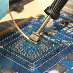
#SMT PCB Job work
Explore tagged Tumblr posts
Visit Tumblr Blog
Explore Tumblr blogs with no restrictions, modern design and the best experience.
Last Seen Tumblr Blogs


Fun Fact
69% of Tumblr users are millennials.
Text
Electronics Technician
JOB ALERT - Electronics Technician Electronics Technician Job Building Electronic PCB Boards using SMT and Soldering.In Rochester, Kent paying £27,000 plus benefits apply via Senex Recruitment. #Hiring #jobsinkent #recruiting #Electronicsjobs #jobs
Electronics Technician job available in Kent. Are you a skilled Electronics Technician / Electronics Operator looking for your next challenge? A medium sized electronics manufacturing company based in the Rochester Kent are searching for a electronics manufacturing professional. If you’re passionate about electronics and want to work in a role where your expertise is truly valued, this could be…
0 notes
Text

Innovative SMT PCB Job Work Signature Cubix Control Systems.
Cubix Control Systems is a leader in SMT PCB jobwork in Delhi NCR, dedicated to accuracy and creativity. Their specialty is using surface-mounting (SMT) techniques to create complex printed circuit boards. By utilizing state-of-the-art equipment and knowledgeable personnel, they guarantee flawless assembly, premium connections, and exceptional electronics production.
#SMTPCBJobwork#SMTPCBJobworkinDelhiNCR#qualitySMTPCBJobwork#affordableSMTPCBJobwork#printedcircuitboardassembly#PCBJobwork#SMTPCBboardmanufacturer#SMTPCBmanufacturer#electronicsproducts#electronicsmanufacturer
0 notes
Text
Reliable, Affordable & Trustworthy Electronics PCB Repair Services & Courses Across Canada/USA
Wireless Training Center is a well-known name in the electronics industry, providing top-notch Electronics PCB repair services in Canada and the USA. With years of experience and expertise, we have established ourselves as one of the best providers of PCB Repair Technician Courses in Canada/ USA.
Wireless Training Center has highly skilled and experienced technicians. Our technicians have been trained to the highest industry standards and are equipped with the latest tools and technology to provide the best possible service and Courses. We can troubleshoot and repair a wide range of PCB issues, including faulty components, damaged circuits, and broken connections.
We use only high-quality components and materials in repairs, ensuring that the repaired PCB will be reliable and long-lasting. Wireless Training Center's PCB repair services are not limited to any specific industry or application. We have experience working with a wide range of PCBs, including those used in the telecommunications, medical, automotive, and industrial sectors. Whether it's a simple repair or a complex overhaul, we have the expertise and experience to get the job done right. This makes us a one-stop-shop for all your electronics needs, whether you're looking for Certified Circuit Board Repair Professionals Training Course or MacBook and iMAC Mother Board Repair Courses in Montreal, Toronto and Vancouver.
Wireless Training Center is also known for its exceptional customer service. We understand that when a customer's PCB is not working, it can have a significant impact on their business operations. That's why we offer quick service to our customers. We also deliver a range of service and course options, including PCB, SMT Rework, reflow and repair training in Canada / USA, to ensure that customers can get their PCBs fixed as quickly and conveniently as possible.
For further info give us a call at (778) 835–2763 or visit us at: https://wirelesstrainingcenter.com/
#PCB#SMT Rework#reflow and repair training in Canada / USA#SMT#THT#Hand Soldering workshops in Canada/ USA#MacBook and iMAC Repair Training Courses in Canada#Cell Phone Repair Course in Calgary#Cell Phone Repair Classes in Mississauga#Circuit Board Certifications#BGA Rework Certifications#Certified Circuit Board Repair Professionals Training Course#Electronics PCB repair services
0 notes
Link
#SMT PCB job work Delhi NCR#SMT plastic Moulding Manufacturers in India#SMT PCB job Work in India#SMT PCB Assembly Equipment Delhi NCR#SMT PCB Job work
0 notes
Text
The Professional PCB Manufacturers

We are providing the finest and high PCB provider of a lot of services and also offer a professional PCB service and a broad range of manufactured PCB which are pretty a lot as good as new. We are various professionals united by way of just one common goal which is to offer one of the best PCB and PCB providers to the purchasers- Pcb
Utilizing high materials and utilizing correct techniques can result in the PCB board being professionally designed. Highly constructed and designed PCB boards will more probably sturdiness long time, with different types of points. They might help them diagnose possible faults on a PCB.
They additionally provide customers good comprehensive services of PCB, smt, PCBA, and components, and that is valuable. This is aimed at the hobbyist who wants a custom PCB for their latest PCB. They will positively be recommending them to all their customers. An incredible PCB service we obtained from us.
They have very trustworthy about the work that must be done and accomplished the job that exceeded my expectations. These PCB services of components and all you'd like is one PCB service of components from our capabilities as per your requirements. For more information, please visit our website https://onepcba.com
0 notes
Text
Reflow ovens

There will be an 8.32 cm spacing between the boards in the oven. To summarize: for our 45 cm board that has a cycle time of 40 seconds, we need a 10-zone oven with a heated tunnel length of 360 cm. These machines vary in size from small boxy. Let’s calculate what it will be:īS = (BL + Spacing)/CT = 1.33 cm/sec => BL+ Spacing = BS x CT => Spacing = BS x CT – BL A SMT reflow oven is an essential machine of the thermal processing of solder for electronics manufacturing. The extra belt speed will allow for a small amount of spacing between the boards. Success! Since 1.33 cm/sec is greater than 1.1125 cm/sec, this 10-zone oven will work. How about the 10-zone oven? Let’s see if the belt speed is greater than the 1.125 cm/sec needed.īS = HTL/Time = 360 cm/270 seconds 1.33 cm/sec Now we can see that the 7-zone oven won’t do the job either. What about a 7-zone oven? Let’s calculate the belt speed for this oven.īS = HTL/Time = 250 cm/270 seconds 0.926 cm/sec The component placers will be presenting a 45 cm board every 40 seconds, so the belt speed needs to be:īS = Board Length/Cycle Time = BL/CT = 45 cm/40 sec = 1.125 cm/sec So if we choose the 5 zone oven the belt speed will be:īelt Speed = BS= Heat Tunnel Length/Time in Heated Tunnel = HTL/Time = 180 cm/270 seconds 0.66 cm/sec SMT Reflow ovens accept PCBs with mounted components in wet solder paste and produce soldered PCBs using convection heating to reflow the solder paste. By studying the reflow profile in above, we see that the amount of time needed in the heated zone is about 4.5 minutes or 270 seconds. Let’s assume that you will be using a typical modern SAC solder paste. Table 1 shows some typical reflow oven metrics: Let’s make some calculations and see if your concerns are justified. But, you are concerned that a 5-zone oven may not have the capacity that is needed to keep up with the component placement machines. Your boss is pressuring you to get another 5-zone oven, as they are cheaper and take up much less space than a 7- or 10-zone oven. The boards are 45 cm long and you expect the cycle time from the component placement machines to be 40 seconds per board. You are putting in a new assembly line to assemble some large boards for which your company just received a 3-year contract. SiP & Heterogeneous Integration & Assembly (HIA).The Indium Corporation & Macartney Family Foundation.Learn more about our products, their applications, find a distributor or access online resources. Our products meet strict regulatory requirements and many are are sustainable, helping protect both people and the planet. MicroCare and its sub-brands, MicroCare Medical, Sticklers and Stereze formulate and blend cleaning coating, lubricating and sterilization fluids used in the manufacture, installation and use of products in the electronics, medical device manufacturing, fiber optic, metal finishing, industrial maintenance and healthcare infection prevention industries. Use with MicroCare lint-free cleaning wipes (MCC-W11) for best results. The noncorrosive fluid is ESD-safe and is safe to use on all metals, synthetics, plastics and elastomers. Money-saving, refillable pump-spray bottle is not TriggerGrip™ compatible. Suitable for use in hand wipe applications or ultrasonic tanks, this cleaner reduces equipment down-time and lowers cleaning costs.Ĭonvenient Packaging Options: The popular 'cubitainers' are easy to store on a shelf and feature a faucet-like valve so the fluid can be dispensed without lifting the container. So, cleaning actually becomes easier over time. During the soldering process, evaporated fluxes as well as gas emissions from solder resist are deposited onto the internal surfaces of. Plus, Reflow Oven Cleaner avoids one of the big problems of alcohol cleaners - the curing and hardening of flux residues in the oven. While I can solder most SMD components by hand, and most components can be bought on break-out boards, I decided that it was time to up my game in the SMD soldering department. This product is so much stronger than IPA alcohol that it slashes oven cleaning times 50% or more while improving cleaning results. Recently, many of my electronics projects have required the use of components that are only available in SMD form. Made with water, alkaloids and proprietary long-chain alcoholsīecause this reflow oven cleaner is nonflammable you can clean the oven while it is still warm, saving time and enhancing the cleaning because warm solvents clean better than cold ones.Cleans all solder paste and flux residues, including RMA, no-clean and lead-free products.Four times faster than IPA (isopropyl alcohol).Activated by the residual heat of the oven.Speeds cleaning of ovens even when warm.Cleaning reflow ovens - in this case, a Heller unit - can be a challenge because of the flux residues that coat the inside of the machines Features:
0 notes
Text
What are the PCBA assembly processes?
With the progress of China's manufacturing capacity, the PCBA industry has also ushered in a climax. In this article, FS Technology will explain to you what technologies Chinese PCBA assembly companies use in assembly.
What is PCB Assembly Process
As we all know, the operation of electronic products is inseparable from the printed circuit board, and PCB is its abbreviation. A PCBA board is assembled from a bare PCB board and electronic components. The bare board refers to the green board, and the electronic components are the objects soldered to the bare board. The bare board cannot function alone. The PCB manufacturing company draws the wiring on the bare board, and the electronic components are electrically connected according to the wiring to function. It can be said that the PCB board is a carrier, and the electronic components are the main body. More differences between PCB and PCBA can be found in FS Technology's blog post PCB vs PCBA .
The PCB assembly process refers to the process in which a turnkey PCB assembly company places components on a bare board through a series of assembly techniques. Generally, surface mount technology or packaging technology is used. That is SMT process and DIP. A qualified turnkey PCB assembly company has the most advanced and professional assembly machines that can work 24 hours a day.
Specific PCBA assembly process
FS Technology provides customized versions, that is, to manufacture suitable PCBA boards according to customer needs. Therefore, we will use different processes according to the size, number of layers, materials, and required functions of the circuit board. What are the pcba processing and assembly processes?FS Technology divides it into the following categories:
Single Side Mount
Single Side Mixed
Double Sided Mounting
Double-sided mixed
Single-sided mounting process
The single-sided mounting process is one of the simplest processes. Generally, the electronic components of this PCB assembly company are mounted components (SMD). FS Technology only needs to stick these components on one side of the pcb board.The specific process is as follows:
Incoming Inspection
Print
Patch
Reflow Soldering
Cleaning
Detect
Single-sided mixing process
Single-side mixing is more difficult than single-side mounting, but even so, most PCB assembly companies can complete the job. The single-sided mixing process refers to mounting different types of PCB components on one side of the bare board, and the components used include mounting and plug-in. The specific process flow is as follows:
Incoming
Detect
Print
Patch
Reflow Soldering
Cleaning
Plugin
Wave Soldering
Cleaning
Detect
Double Sided Mounting Process
The double-sided mounting process means that the components are all mounted components, and the components are mounted on both sides of the PCB board, commonly known as double-sided PCB boards.The specific mounting process is as follows:
Incoming Inspection
A side printing of pcb board
Patch
Reflow Soldering
Flip
PCB board B side printing
Patch
Reflow Soldering
Cleaning
Detect
Double-sided mixing process
The double-sided mixing process refers to components that are both mounted and plug-in, and components are mounted on both sides of the pcb board. This process is very difficult, and few turnkey PCB assembly companies in China can complete it. The specific process is as follows:
Incoming Inspection
A side printing of pcb board
Patch
Reflow Soldering
PCB board B side plug-in
Lead bend
Flip
B-side point patch glue
Patch
Drying
Flip
Wave Soldering
Cleaning
Detect
The above content is a simplified version of the pcba processing and assembly process. The specific processing process can be found in the FS technology blog. Here, FS Technology reminds practitioners in the PCB industry that the PCBA processing and assembly process is very complicated, but every process is indispensable, which directly affects the quality of the assembly. When your project requires a turnkey PCB assembly company, you need to investigate the company's comprehensive content, PCB manufacturing capabilities and assembly capabilities. FS Technology has been doing very well in the past ten years of work, especially the assembly. FS Technology focuses on smt patch proofing, PCB proofing, component procurement and other services. It can be said that it is the best turnkey assembly company in China.
1 note
·
View note
Text
AOI jobs in BAwal Haryana
AOI machine operator jobs in BAwal Haryana
QF:#Polytechnic Diploma , iti #Electronics
#Vacancy :-5
Salary :- 16000 to 22000
Exp:- 2 to 4 year
Gender:- male
whatsapp sent 9887904788) no call
Department:- Quality
Candidate working any Automotive Electronics Industry #aoi #smt #bawal #productions #devplacement #jobseeker #jobhiring #diploma #pcb #permanent #vacancy #electronics #operations #haryana #surface #mount #technology #operator
Interview next week
Plz Cv Send Me
9887904788
https://t.me/placementdev,
https://www.facebook.com/groups/DevPlacement,
https://twitter.com/DevPlacement,
www.devplacement.com,
https://www.linkedin.com/company/devplacemet
Private limited company jobs in BAwal Haryana
Mnc company jobs in BAwal Haryana
Electronic company jobs in BAwal Haryana
Company list in BAwal Haryana
AOI-Operator Omron 3D operation for our Bawal location

0 notes
Text
In the developing world of electronics production, the initial of each tool lies inside its Printed Circuit Board (PCB). The complicated assemblies of electronic components have become the backbone of infinite current gadgets, from smartphones to car manipulation systems. Behind the scenes, a specialized enterprise known as Surface Mount Technology (SMT) PCB Job work performs a pivotal function in bringing those circuit forums to lifestyles.
SMT PCB Job work, frequently referred to as PCB meeting, is a meticulous and noticeably specialized procedure in electronics production internationally. This article delves into the world of SMT PBC job work, shedding mild on its importance and the craftsmanship concerned.
0 notes
Text
Industrial PCB Repair Technician Courses for Beginners

Are you tired of being underpaid and overworked at your job? Do you hate being thought of merely as a machine operator? Are you ready to take control of your life and pursue your real passion? You can do this by gaining an Industrial PCB Repair Technician Certification through our course! Wireless Training Center can help you. Our PCB Repair Technician Courses in Canada/ USA will teach you the basics of a career repairing PCBs in a factory setting. Whether you're a student looking to get ahead in your studies, an adult looking to start a brand new career, or a person just bored one afternoon, our course will give you the know-how you need to be a successful PCB Repair Technician!
Not only that, but you'll be able to work in a number of different sectors from shipbuilding to waste management! You can even work for yourself as a freelance PCB Repair Technician! Our Electronics PCB repair services Courses include lectures, labs, and projects that will give you hands-on experience with using different tools and techniques as well as some theory about how these things work together. The coursework is customized for each student based on their background so that no one else has the same learning experience. Our motto is "dedication towards excellence" because we believe that if an individual wants something badly enough then they would never give up until they get it.
Our Industrial PCB Repair Technician Course for Beginners is a comprehensive program that provides a foundation for a career as a PCB technician. Through the course, you will learn the necessary skills for completing repairs on any Industrial PCB, even those with the most challenging components and multi-layered boards. Here you will also get SMT, THT, and Hand Soldering workshops in Canada/ USA from our experienced instructors, so you can start a career in this growing field that is in high demand across many industries. If you have an interest in working with PCBs, our PCB Repair Technician course isthe right choice for you! To learn more about our PCB Repair Technician course, visit www.wirelesstrainingcenter.com
#SMT#THT#Hand Soldering workshops in Canada/ USA#PCB#SMT Rework#reflow and repair training in Canada / USA
0 notes
Photo

Printed Circuit Board Assembly is the nucleus of Cubix’s activities and the foundation of our success. Use of the latest technologies on surface mount assemblies, combined with a craftsman’s concern for perfection, enables our production team to achieve a high level of throughput and yield for the most complex and demanding PCB Assemblies.
0 notes
Link
Jayshree Instruments provides PCB assembly services in Ahmedabad, India. Including different process such as surface mount technology (SMT), through hole technology, and SMD PCB assembly services.
1 note
·
View note
Text
Low cost PCB assembly
The utility model relates to the technical field of PCB board, particularly to a low-cost PCB assembly with convenient assembly. Background technology: PCB board, also known as the printed circuit board, is the electrical connection of electronic components. The main advantage of using the circuit board is to greatly reduce wiring and assembly errors and improve automation and production labor rate. At present, according to the number of PCB layers, PCB can be divided into a single panel, double-sided board, four-layer board, six-layer board, and other multilayer circuit boards. The PCB board structure is generally composed of a substrate layer and a conductive layer above the substrate layer, and the substrate layer is an insulating layer. In applying the PCB board, the corresponding electronic components will be welded on the electronic component pad on the PCB board’s conductive layer. In the existing technology, the connection between electronic components and the conductive layer is mostly by welding, which has the defects of a cumbersome process, inconvenient assembly, and high production cost. Moreover, the pins of electronic components are fixed on the pad by soldering tin. There may be false soldering. Also, due to the poor thermal conductivity of the resin composite material of the insulating layer, the heat generated by the work of electronic components is mainly transmitted to the external air through the conductive layer’s copper foil. However, the thickness of the copper foil is minimal, and the thermal conductivity is limited. Therefore, it is usually necessary to set a heat dissipation layer at the insulation layer’s bottom. In the existing technology, the heat dissipation layer is generally connected with. However, these methods have the defects of inconvenient assembly.
Both sides of the heat absorbing and cooling material layer are provided with clasps, and the two ends of the base material layer are provided with clamping blocks for connecting with the buckle; The plurality of heat dissipation via holes is inclined. The longitudinal section of the inserting groove is set as U-shaped. The slot of the socket is provided with four elastic conductive sheets for sealing the slot. The inclination angle of the heat dissipation through-hole is set at 5 degrees to 10 degrees. Preferably, the inclination angle of the heat dissipation through-hole is set as 8 degrees. Both ends of the snap are provided with expanded shrapnel. Two expanded shrapnel are relatively arranged at the two ends of the snap.
With the continuous development of science and technology, SMT processing gradually comes into our lives and is gradually known by more people. It belongs to a new type of electronic components, which is more common in the current society. So how can we reduce the production cost of PCBA and do a good job in quality control? The following is a brief introduction made by DEASPCB, a professional PCB assembly factory
For more details on our products and services, please feel free to visit us at: Quick Turn PCB Fabrication, Low Cost PCB Assembly, PCB Fabrication and assembly, China pcb assembly, Quick Turn PCB Assembly.
0 notes
Text
How To Perform Visual Inspection After PCB Assembly?
Visual inspection is a process that must be carried out after PCB Assembly. As you probably know, visual inspection is mainly for the appearance of PCB components and solder joints, and which is also a timely feedback to PCB Assembly as well as improve the soldering of SMT Assembly and product quality.

>Basic working conditions for visual inspection
1. Working conditions: Temperature [ 18°C to 28°C], Humidity [35%~75%];
2. Operation object: All assembled PCB boards;
3. Operator: With certain general SMT and DIP welding status discrimination ability;
4. Job responsibilities: Compare and screen bad welds, write down bad marks, and fill in the corresponding forms.

> Materials required for visual inspection
1. PCBA: Quantity;
2. Label and record of bad product: 1 copy;
3. Anti-static wrist: 1;
4. Anti-static gloves: 1 pair;
5. Anti-static rotating jig: Several.

>Visual inspection procedure
1. Wear anti-static clothes, anti-static wrists and gloves then sit down;
2. Paste the PCBA serial numbers to follow-up quality tracking.
3. Hold the PCBA with both hands and keep the tilt angle of 45°. From left to right, scan key components and connectors line by line from top to bottom to see if there is any bad soldering.
4. Take the long side of the PCBA as the axis and rotate at will at a certain angle to observe whether the key components have bad angles of buoyancy, skew, missing welding and missing welding.
5. If a poorly welded component or connector is found and cannot be determined by itself, the on-site management should be consulted to confirm whether it is qualified, and no judgment should be made at will.

6. When the defective product is found to be obviously defective, the label of the defective product is only the label. Please note that the label of the defective product points to the defective arrow.
7. Flip to the other side of the PCBA and focus on the soldering quality of the connector solder joints: whether there is even tin, missing solder, little solder joints, cold soldering, tin tip, dirt, etc., and abnormal adhesion is found The defective label is distinguished and placed on the shelf of the defective product.
8. Visually inspect key components several times and place abnormal products on the shelf of qualified products.
9. Every 10 PCBA boards should be carried out in groups, and the relevant records should be verified for completeness and transferred to the next process if there is no omission.
10. Fill in the bad product record list, and fill in the description of the bad phenomenon according to the serial number.
11. Defective products should be placed in the specified relatively fixed position, and clearly marked, not to be confused.
https://www.grande-pcba.com/
0 notes
Text
Find advanced Forensics Micro Soldering Course for Law Enforcement at wirelesstrainingcenter.com!!!

In this blog we want to let you know about Wireless Training Center that offers outstanding solution for the Two Way Radio Repair Training Course.
Two-way Radio Repair Technicians, Sales Engineers, Service Technicians, Contractors or beginners who wants to work in the two-way radio repair industry. A two-way radio is a radio that can both transmit and receive a signal (a transceiver), unlike a broadcast receiver which only receives content. Two-way radio systems usually use a single radio channel and operate in a half-duplex mode: the user can talk, or he can listen, but not at the same time.
Wireless Training Center provides instructor-led in-classroom and on-site training courses and workshops in smart phone repair, wireless sales, RF and wireless technologies since 2013. Training is provided to wireless dealers, mobile phone repair stores, online stores, schools and individual students. All our instructors are experienced professionals with 15 plus years of industry experience.
We design, develop and deliver tailor-made customized training courses and workshops for new employees. Customized training programs such as, Forensics Micro Soldering Course for Law Enforcement are designed to make a difference in your bottom line, whether your organization is creating jobs, investing in technology, or streamlining processes for efficiency.
This instructor-led, Advanced Forensics Micro Soldering Course for Law Enforcement course is designed for experienced forensics officers and technicians who have basic cell phone troubleshooting skills. This course can cover advanced board-level soldering, Micro-soldering, troubleshooting and diagnostics, IC chip replacement, reflow, re-balling iPhone, Samsung Galaxy, LG, iPad Mini and more.
This course can be combined with Advanced Micro Soldering Specialist Course Level 4 and IC Specialist Course Level 5. We also bring our courses to your school, train your students; provide all necessary material, phones, equipment, tools, and supplies for hands-on exercises at very attractive rates. Certificates are awarded after the course completion.
This instructor-led, Advanced Micro soldering, hands-on course instructor has 15 plus years of Smartphone repair, BGA Rework, BGA Reflow, SMT Rework, Advanced Micro PCB Soldering experience. Forensics officers, forensics technicians, law enforcement officers, forensics analysts should attend this course.
For further details please visit our website.
0 notes
Photo

Cubix control system is basically a certified Electronics manufacturing services company which offer high quality, innovative and cost-effective product. This company provides full suite services in avant-grade sectors such as consumers electronics, automotive, telecom, IT peripherals, lighting, home appliances, defence etc. It is located in Noida with total production area of 35,000 sq. ft.
#SMT PCB job Work in India#SMT PCB job work Delhi NCR#PCB Assembly Manufacturers Service in India#Electronics Assembly Manufacturer in India#Plastic Moulding Manufacturers in India#Box Build Assembly Manufacturer in India#Electronics Manufacturing Services Export in India#SMT PCB Assembly Equipment Delhi NCR
0 notes