#Integrated Circuit (IC) manufacturers
Explore tagged Tumblr posts
Visit Tumblr Blog
Explore Tumblr blogs with no restrictions, modern design and the best experience.
Last Seen Tumblr Blogs


Fun Fact
69% of Tumblr users are millennials.
Text
What Are LED Driver ICs?
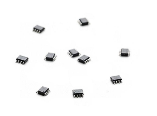
LED Driver ICs are integrated circuits designed specifically to manage and control the power and brightness of LED lighting systems. They play a key role in power conversion, current regulation, and PWM (Pulse Width Modulation) control, ensuring that LED lights operate in an efficient and stable manner.
Get more info: About LED Driver ICs
#electronics#integrated circuits#semiconductor#components#electronic#module#electronic devices#chips#manufacturing#led driver#led display#ics
0 notes
Text
2025 Monthly Topic Poll
As mentioned previously, 2024 is rapidly coming to an end - and that means the end of the 2024 daily posts! Next year, every three months (March, June, Sept, and Dec) I’ll be posting about an MSE topic at least every other day - and it's time to vote on topics! Top four topics will win, unless it's ambiguous, in which case I'll run another poll (or if there's no interest in any of them!)
More explanation for each topic is under the cut:
Acoustics and sound: All about acoustics in materials science, and also the materials science of acoustics, anything from ultrasonic testing to the science of musical instruments.
Atoms: The science of things at the atomic level; electron energy levels, protons, neutrons, isotopes, etc.
*Careers: This one would require input from followers, but would include posting on what kind of careers exist that involve materials science, however directly.
Color: The sources of color in the world around us. Incandescence, color centers, structural color, etc.
Computational materials science: Different techniques and methods of computational materials science
Data: Presenting data, managing data, collecting data, etc.
Elemental groupings: What are the halogens? The refractory elements? Noble metals?
Energy sources: Where are we drawing energy from? What types of solar power exist? What's the status of tidal energy generation?
Integrated circuit (IC) failure analysis: Exactly what it says on the tin, failure analysis of integrated circuits.
Materials maturity levels: Also manufacturing readiness levels; how do we go from testing a new material in the lab to mass production?
Property prefixes and suffixes: Is piezoelectricity the only piezo- property there is? What is the prefix tribo-? How many types of magnetism are there?
Transmission electron microscopy: All about the ins and outs of how transmission electron microscopy works and the different varieties and forms of it.
32 notes
·
View notes
Note
wait you made a genesis controller that's so fucking cool
Hell yeah I did!! I was making custom arcade sticks for a while with my best friend. We made one as a proof of concept for a decently popular speedrunner and when he used it on stream a number of other streamers contacted us looking for controllers. One was a classic Sonic runner that asked for a Genesis controller and I was like "Sure, that sounds like a fun challenge!"
It wound up being... Ultimately not that bad?? But it required a lot of experimentation and learning on my part the details of which are about to be inflicted upon you because you dared to ask
When I started I looked at the Genesis controller pinout my first thought was "oh, that's super easy" - it's 9 pins: 2 that carry power, 6 that carry data, and one SELECT line that changes which pins represent which buttons. This is a hilariously easy C program to write so I got the Pico SDK set up and cranked it out, flashed it using my janky homemade picoprobe carrier, and immediately ran headfirst into problems.

See, my thinking was along the lines of "The Pico runs at like 8x the clockspeed of the Genesis, I just need some level shifters to convert between 3V and 5V signals and we're golden" and that was... Actually mostly true. However, every like 20-30 seconds it would produce either phantom inputs or drop out entirely for half a second or so, which is just laughably unacceptable for speedrunning purposes.
I tried pursuing that implementation for a while - down to comparing signals from my controller and a stock Genesis controller with an oscilloscope - before I ultimately decided that it wasn't worth the effort. I think the final straw was that it was basically working in game but the everdrive menu wouldn't work with it at all?

It was at this time that I finally decided to crack open an old Genesis controller and look at what integrated components (ICs) it used to try to reverse the circuit. The one I had was worthless - after copycat controllers started showing up on the market back in the day SEGA switched all their official controllers to use a single proprietary chip that they produced specifically for this purpose. They even put a glob of some dense cured resin shit over the chip and the traces around it to make it impossible to lift off the board or reverse.
I found a couple grainy scans online of REEEEEEALLY old controller models that and could sus out a multiplexer chip and that's about when things started making sense to me. Previously I had only worked with digital controller protocols like xinput (Xbox/PC) or joybus (N64/GameCube) but that was a level of sophistication only achieved later in the development of game consoles - there is no protocol on the Genesis.
There are 9 pins on the Genesis main board (18 for both controller inputs) that are connected directly to the pins on the controller port. Your controller takes a Long Ass Wire and connects those pins to buttons on the gamepad, with a multiplexer sitting in between so it can swap out a couple buttons based on the SEL line. It didn't matter how fast my chip ran because 1. This is gonna be a noisy signal and measuring it digitally is going to be imperfect, and 2. Literally any latency whatsoever is a problem because this is going to be read at a hugely variable rate. This has to be implemented with logic gates.
For those of you that have a college education (in say, comp sci or comp eng or electrical eng or mech eng) this is likely not that much of a challenge. For me, as a professional software engineer, expressing the logic was trivial:

(I know I probably could've done that with just NAND gates (and the inverter is COMPLETELY unnecessary) but a girl loves easy-to-read circuit diagrams that directly reflect the intended logic)
But manufacturing the damn thing?? THAT was the hard part. My dumb (white, self-taught) ass had never worked with ICs before, so my first draft was literally just sticking all of these together with no resistors or capacitors in there whatsoever. I had basically just made an antenna - moving the controller around in space (or bearing near enough to other electronics) caused voltage fluctuations which resulted in erratic signals being sent to the console.
My SECOND draft however - after consulting with an Actual Electrical Engineer ™ and learning the benefits of capacitors and resistors in logic circuit design - worked fucking great. According to EE friend it was slightly overbuilt - I had given each IC its own power input smoothing capacitor located right next to those pins when just one would likely suffice, and similarly every input pin got its own pull-up resistor - but I was 100% okay with that. Overbuilt is better than underbuilt and this is a handmade low-volume good, a couple cents on electrical components made no meaningful budget impact.
One "oh god fuck doing this by hand" and run of FreeRouting's Auto Router later we had ourselves a PCB layout!

I placed an order for 3 of those from our good friends at OshPark and then it was just a matter of assembly! Soldering it together was easy as hell, the final product ended up looking this (short a few capacitors I was still testing to see if I needed)

Then it was time for assembly!! The client requested black acrylic panels to kind of resemble a B0XX so I took our CAD model of the controller and I added circuit mounting holes to the bottom panel, cut each panel out with my laser cutter, and started piecing the panel joints together with a tight friction fit. To seal the joints I carefully filed the seams of each edge until I had a rounded and near-seamless corner filled with ground acrylic and then used a very fine plastics glue to flood the micro gaps in there and give it more long term sticking power. Notably I didn't do this on the bottom panel as it's meant to be popped on and off by the user if they wanted to replace the buttons or wiring harnesses or something.
Then...it was done!! Because of the raw amount of fuckery involved in this process (and the fact that this wasn't my main source of income/I was selling my house/meeting my fiance/MANY other things) it took about a year between me receiving the commission and actually shipping the finished product, but I'm really proud to say that we did do it and the client LOVES it!!


#aripost#asks#on the one hand I'm sorry for inflicting this on everyone's dash#but on the other hand I'M REALLY FUCKIN PROUD OF THIS THING AND YOU HAVE TO LOOK AT IT OKAY
10 notes
·
View notes
Note
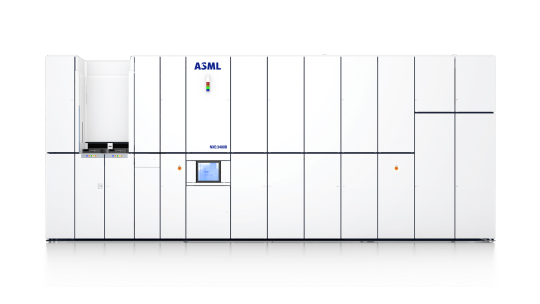
how can an IC fab stepper motor move only 10nm per ste
for reference, this question is talking about machines called steppers that are used in the production of integrated circuits (you know, computer chips)
integrated circuit fabrication is, without a doubt, the most complex and involved behaviour humans have ever exhibited, and we're not going to go into it today, it is way too much. it happens in fabrication facilities which are vast campuses of buildings on the order of dozens and dozens of city blocks. to even get in most of those buildings you even need to wear a special bunny suit. anyways, there is obviously a lot of complicated, expensive equipment involved, but the one that takes the cake is the stepper. it's where the magic happens.
when people talk about chip sizes and moore's law and all that, they're talking about the smallest features we can print onto a chip, usually the transistor gate length. this is on the order of tens of nanometers currently. in order to achieve that, we have to have some device capable of working accurately & precisely down to the tens of nanometers. this is the stepper. it aligns photomasks accurately to such a degree for exposure. that is "the magic" i mentioned
the good modern steppers used in the production of, e.g. the intel i7 CPU in your computer are made by one company. they run about $200mm USD. lol:
with the cowling off:
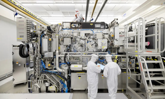
inside this thing, photomasks are physically aligned, and their alignment has to be accurate to within nanometers, like i said. the straightforward answer to this question, is that such alignment is done with linear motors. we just build them to an insane degree of precision, and then control and drive them with ultra-high-accuracy electronics. fundamentally speaking, just like with a normal induction motor, you can measure the electrical characteristics of the windings during operation and deduce details about your rotor (or in this case, where your actuator is in space). if you use ultra-high-precision electronics, you get accordingly precise details. (like, where on the X axis your actuator is sitting)
these sorts of extremely niche motors, of course, also need a whole daughter industry to design and manufacturer. the stepper vendor doesn't just do that in-house. i found one such company. these things, or, these other things would be examples
139 notes
·
View notes
Text

The Birth of an Industry: Fairchild’s Pivotal Role in Shaping Silicon Valley
In the late 1950s, the Santa Clara Valley of California witnessed a transformative convergence of visionary minds, daring entrepreneurship, and groundbreaking technological advancements. At the heart of this revolution was Fairchild Semiconductor, a pioneering company whose innovative spirit, entrepreneurial ethos, and technological breakthroughs not only defined the burgeoning semiconductor industry but also indelibly shaped the region’s evolution into the world-renowned Silicon Valley.
A seminal 1967 promotional film, featuring Dr. Harry Sello and Dr. Jim Angell, offers a fascinating glimpse into Fairchild’s revolutionary work on integrated circuits (ICs), a technology that would soon become the backbone of the burgeoning tech industry. By demystifying IC design, development, and applications, Fairchild exemplified its commitment to innovation and knowledge sharing, setting a precedent for the collaborative and open approach that would characterize Silicon Valley’s tech community. Specifically, Fairchild’s introduction of the planar process and the first monolithic IC in 1959 marked a significant technological leap, with the former enhancing semiconductor manufacturing efficiency by up to 90% and the latter paving the way for the miniaturization of electronic devices.
Beyond its technological feats, Fairchild’s entrepreneurial ethos, nurtured by visionary founders Robert Noyce and Gordon Moore, served as a blueprint for subsequent tech ventures. The company’s talent attraction and nurturing strategies, including competitive compensation packages and intrapreneurship encouragement, helped establish the region as a magnet for innovators and risk-takers. This, in turn, laid the foundation for the dense network of startups, investors, and expertise that defines Silicon Valley’s ecosystem today. Notably, Fairchild’s presence spurred the development of supporting infrastructure, including the expansion of Stanford University’s research facilities and the establishment of specialized supply chains, further solidifying the region’s position as a global tech hub. By 1965, the area witnessed a surge in tech-related employment, with jobs increasing by over 300% compared to the previous decade, a direct testament to Fairchild’s catalyzing effect.
The trajectory of Fairchild Semiconductor, including its challenges and eventual transformation, intriguingly parallels the broader narrative of Silicon Valley’s growth. The company’s decline under later ownership and its subsequent re-emergence underscore the region’s inherent capacity for reinvention and adaptation. This resilience, initially embodied by Fairchild’s pioneering spirit, has become a hallmark of Silicon Valley, enabling the region to navigate the rapid evolution of the tech industry with unparalleled agility.
What future innovations will emerge from the valley, leveraging the foundations laid by pioneers like Fairchild, to shape the global technological horizon in the decades to come?
Dr. Harry Sello and Dr. Jim Angell: The Design and Development Process of the Integrated Circuit (Fairchild Semiconductor Corporation, October 1967)
youtube
Robert Noyce: The Development of the Integrated Circuit and Its Impact on Technology and Society (The Computer Museum, Boston, May 1984)
youtube
Tuesday, December 3, 2024
#silicon valley history#tech industry origins#entrepreneurial ethos#innovation and technology#california santa clara valley#integrated circuits#semiconductor industry development#promotional film#ai assisted writing#machine art#Youtube#lecture
8 notes
·
View notes
Text
Introducing Samsung 24GB GDDR7 DRAM For AI Computing

24GB GDDR7 DRAM
Future AI Computing: Samsung Launches 24GB GDDR7 DRAM. It sets the standard for graphics DRAM with its industry-leading capacity and performance of over 40Gbps.
First 24-gigabit (Gb) GDDR7 DRAM from memory pioneer Samsung was revealed today. Next-generation applications benefit from it’s speed and capacity. Data centers, AI workstations, graphics cards, gaming consoles, and autonomous driving will employ the 24Gb GDDR7 because to its high capacity and excellent performance.
“By introducing next-generation products that meet the expanding demands of the AI market, it will maintain to leadership position in the graphics DRAM market.” The 5th-generation 10-nanometer (nm)-class DRAM used in the 24Gb GDDR7 allows for a 50% increase in cell density while keeping the same package size as the previous model.
The industry-leading graphics DRAM performance of 40 gigabits per second (Gbps), a 25% increase over the previous iteration, is achieved in part by the advanced process node and three-level Pulse-Amplitude Modulation (PAM3) signaling. The performance of it may be further improved to 42.5 Gbps, contingent on the environment in which it is used.
Applying technology previously used in mobile devices to graphics DRAM for the first time also improves power efficiency. Power efficiency may be increased by more than 30% by reducing needless power use via the use of techniques like dual VDD design and clock control management.
The 24Gb GDDR7 uses power gating design approaches to reduce current leakage and increase operational stability during high-speed operations.
Major GPU customers will start validating the 24Gb GDDR7 in next-generation AI computing systems this year, with intentions to commercialize the technology early the next year.
GDDR6 vs GDDR7
Compared to the current 24Gbps GDDR6 DRAM, GDDR7 offers a 20% increase in power efficiency and a 1.4-fold increase in performance.
Today, Samsung Electronics, a global leader in cutting-edge semiconductor technology, said that it has finished creating the first Graphics Double Data Rate 7 (GDDR7) DRAM in the market. This year, it will be first placed in important clients’ next-generation systems for validation, propelling the graphics market’s future expansion and solidifying Samsung’s technical leadership in the industry.
Samsung’s 16-gigabit (Gb) GDDR7 DRAM will provide the fastest speed in the industry to date, after the introduction of the first 24Gbps GDDR6 DRAM in 2022. Despite high-speed operations, new developments in integrated circuit (IC) design and packaging provide more stability.
With a boosted speed per pin of up to 32Gbps, Samsung’s GDDR7 reaches a remarkable 1.5 terabytes per second (TBps), which is 1.4 times that of GDDR6’s 1.1 TBps. The improvements are made feasible by the new memory standard’s use of the Pulse Amplitude Modulation (PAM3) signaling technique rather than the Non Return to Zero (NRZ) from earlier generations. Compared to NRZ, PAM3 enables 50% greater data transmission in a single signaling cycle.
Notably, using power-saving design technologies tailored for high-speed operations, the most recent architecture is 20% more energy efficient than GDDR6. Samsung provides a low-operating voltage option for devices like laptops that are particularly concerned about power consumption.
In addition to optimizing the IC design, the packaging material uses an epoxy molding compound (EMC) with good thermal conductivity to reduce heat production. Compared to GDDR6, these enhancements significantly lower heat resistance by 70%, ensuring reliable product performance even under high-speed operating settings.
GDDR7 Release Date
According to Samsung, commercial manufacturing of their 24GB GDDR7 DRAM is scheduled to begin in early 2024. Although the precise public release date is yet unknown, this year’s certification process with major GPU manufacturers is already under way. With the availability of next-generation GPUs that will support the new memory standard, GDDR7 DRAM is now expected to be readily accessible in the market by 2024.
Read more on Govindhtech.com
#Samsung#Samsung24GBGDDR7#GDDR7DRAM#24GBGDDR7DRAM#DRAM#GDDR6DRAM#GPU#AI#News#Technews#Technology#Technologynews#Technologytrends#govindhtech
3 notes
·
View notes
Text
What is PCB Assembly ?
PCB Assembly manufacturer - Hitech Circuits Co., Limited
It’s the step in the manufacturing process in which you populate a blank board with the electronic components needed to make it into a functional printed circuit board. It’s these components that make a board into the circuit that enables an electronic product to function. PCB assembly typically takes place via one of two processes:
1. Surface-mount technology
SMT: SMT stands for “Surface Mount Technology“. The SMT components are very small sizes and comes in various packages like 0201, 0402, 0603, 1608 packages for resistors and capacitors. Similarly for Integrated circuits ICs we have SOIC, TSSOP, QFP and BGA.
The SMT components assembly is very difficult for human hands and can be time taking process so it is mostly done by automated pick and place machine.
2. Through-hole manufacturing
THT: THT stands for “Through hole Technology”. The components with leads and wires, like resistors, capacitors, inductors, PDIP ICs, transformers, transistors, IGBTs, MOSFETS are example.
The component has to be inserted on one side of PCB and pulled by leg on other side and cut the leg and solder it. The THT components assembly is usually done by hand soldering and is relatively easy.
Printed Circuit Board Assembly Techniques
There are only two common PCBA techniques available for use by a PCB designer. The methods are:
1. Automated PCB Assembly Techniques
Generally, this technique employs the use of state of the art machines, which are fully automatic. For example, the surface mount components are worth positioning with the aid of an automated pick and place machine.
Again, reflow soldering is commonly for surface mount components usually done in a reflow oven. An automated solder stencil is also used to apply the solder paste on the PCB.
Finally, high tech inspection machines are used to confirm and check the quality of the PCBA. Some of which include: Automated optical inspection machine (AOI), X-ray inspection machines, etc.
Above all, due to the precise monitoring, control of soldering, no human input and versatile machines.
This technique ensures utmost efficiency, output consistencies, and limits defects.
2. Manual PCB Assembly Techniques
This method is favorite for use with through-hole parts, which needs manual placement on the board. Besides, with these through-hole parts, it’s advisable you use wave soldering. Note that in the through- hole assembly process, you need to place the components and electronics on the PCB.
After that, you use wave soldering to solder the leads. Typically, you will need an individual to insert a component into a marked PTH. Once done, transfer the PCB to the next station where the next person will be on standby tasked with fixing another part.
What are the Benefits of SMT PCB Assembly?
SMT assembly provides many benefits and some of them are as follows:
It can be used to incorporate small components.
In SMT, the components can be placed on both sides of the board.
It assures high component densities.
Fewer holes need to be drilled for surface mounting than through-hole.
It require low initial costs and time for setting up the mass production.
SMT is the simpler and faster-automated assembly when compared to through-hole.
Errors regarding the component placement can be easily rectified.
Surface mount PCBs feature strong joints, which can easily withstand vibrations.
What are the techniques used in Surface Mount Technology?
There are several techniques for the reflow process. After applying the solder paste or a flux mixture on the board and after placing the components, the boards are conveyed to a reflow soldering oven. The techniques used for reflowing soldering include infrared lamps, hot gas convection, fluorocarbon liquids with a high boiling point, and so on.
What are the different testing methods used in SMT PCB Assembly?
Hitech Circuits as the PCB assembly manufacturer, we perform the following testing and inspection to ensure the quality of surface mount PCBs.
Automated Optical Inspection (AOI): This is performed before and after the soldering to identify the component placement, presence, and solder quality.
X-ray Testing: In this type of testing, the operator relies on the X-ray images of the PCB to check the solder joints and lead-less components such as Quad Flat Packs and ball grid arrays, which are generally not visible to naked eyes.
In-Circuit Testing (ICT): This method is used to detect manufacturing defects by testing the electrical properties in the SMT Assembly.
What type of files or documents should I send for SMT PCB Assembly?
Gerber Files: The file contains all details of physical board layers including solder masks, copper layers, drill data, legends, and so on.
Bill of Materials (BOM): This contains information on the list of items needed for the PCB manufacturing and the instructions of manufacturing.
Pick and Place File: This file contains information on all components to be used in the PCB design and their rotation and X-Y coordinates.
The whole process of PCB Assembly
1. Bare board loader machine
The first step in the PCB assembly is to arrange the bare boards on the rack, and the machine will automatically send the boards one by one into the SMT assembly line.
2. Printing solder paste
When PCB on the SMT production line, firstly, we have to print solder paste on it, and the solder paste will be printed on the pads of the PCB. These solder pastes will be melt and solder the electronic parts to the circuit board when it passes through the high-temperature reflow oven.
In addition, when testing new products, some people will use film board/adhesive cardboard instead of solder paste, which can increase the efficiency for adjusting the SMT machines.
3. Solder paste inspection machine(SPI)
Since the quality of solder paste printing is related to the quality of welding of subsequent parts, some SMT factories will use optical machine to check the quality of solder paste after printed the solder paste in order to ensure stable quality. If there any poorly printed solder paste board, we will wash off the solder paste on it and reprint, or remove the excess solder paste if there is redundant solder paste on it.
4. High speed SMT machine
Usually, we will put some small electronic parts (such as small resistors, capacitors, and inductors) to be printed on the circuit board first, and these parts will be slightly stuck by the solder paste just printed on the circuit board, so even if the speed of printing is very fast and the parts on the board will not fall away. But large parts are not suitable for use in such high speed SMT machines, which will slow down the speed of small parts assembly. And the parts will be shifted from the original position due to the rapid movement of the board.
5. Universal SMT machine
Universal SMT machine is also known as "slow machine", it will be assembled some large electronic components, such as BGA IC, connectors, etc., these parts need more accurate positions, so the alignment is very important. Use a camera to take a picture to confirm the position of the parts, so the speed is much slower than High speed SMT machine we taked before. Due to the size of the components here, not all of them are packed in tape and reel, and some may be packed in trays or tubes. But if you want the SMT machine to recognize the trays or tube-shaped packaging materials, you must configure an additional machine.
Generally, traditional SMT machines are using the principle of suction to move electronic parts, and in order to place the parts successfully, and there must be the flat surface on these electronic components for the suction nozzle of the SMT machine to absorb. However, for some electronic parts don’t have a flat surface for these machines, and it is necessary to order special nozzles for these special-shaped parts, or add a flat tape on the parts, or wear a flat cap for thees electronic parts.
6. Manual parts or visual inspection
After assembled all parts by the high speed SMT machine or Universal SMT machine and before going through the high-temperature reflow oven, and we will set up a visual inspection station here and to pick out the deviation parts or missing components boards etc., because we have to use a soldering iron to repair if there are still defectives boards after passing the high-temperature oven, which will affect the quality of the product and will also increase the cost. in addition, for some larger electronic parts or traditional DIP parts or some special reasons cannot be processed by the SMT machine before, they will be manually placed on pcb here.
7. Reflow oven
The purpose of reflow oven is to melt the solder paste and form a non-metallic compound on the component feet and the circuit board, that means to solder electronic components on the circuit board. The temperature rise and fall curves often affect the soldering quality of the entire circuit board. According to the characteristics of the solder materials, usually the reflow oven will set the preheating zone, soaking zone, reflow zone, and cooling zone to achieve the best soldering effect.
For example, the melting point for SAC305 solder paste with lead-free is about 217°C, which means that the temperature of the reflow oven must be higher than the melting points to remelt the solder paste. What's more, the maximum temperature in the reflow furnace should not exceed 250°C, otherwise many parts will be deformed or melted because they cannot withstand such a high temperature.
Basically, after the pcb passed through the reflow oven, the assembly for the entire circuit board is almost complete. If there are hand-soldered parts, we need to transfer to DIP process, and then we have to check the quality after reflow oven by QC department.
8. Automatic optical inspection(AOI)
The main purpose of setting up AOI is because some high density boards can’t be process the following ICT test, so we used AOI inspection to replace it. But even using AOI inspections, there still have the blind spots for such checking, for example, the solder pads under the components cannot be checked by AOI. At present, it can only check whether the parts have side standing issue, missing parts, displacement, polarity direction, solder bridges, lack of soldering etc., but cannot checking the BGA solderability, resistance value, capacitance value, inductance value and other components quality, so far AOI inspection can’t completely replace ICT test.
Therefore, there is still some risk if only AOI inspection is used to replace ICT testing, but ICT test is also not 100% make sure the good quality, we suggest these two ways can be combined with together to make sure the good quality.
9. PCB unloader machine
After the board is fully assembled, it will be retracted to the unloder machine, which has been designed to allow the SMT machine to automatically pick and place the board without damaging the quality for PCB.
10. Visual inspection for finished products
Normally there will be a visual inspection area in our SMT production line whether there is an AOI station or not, and it will help to check if there are any defectives after completed assembled the pcbs. If there is an AOI station, it can reduce the visual inspection worker on our SMT line, and to reduce the potential cost, and because it is still necessary to check some places that cannot be judged by AOI, many SMT factories will provide the mainly visual inspection templates at this station, which is convenient for visual inspection worker to inspect some key parts and polarity for components.
11. DIP process
DIP process is a very important process in the whole PCBA processing, and the processing quality will directly affect the functional for PCBA boards, so it is necessary to pay more attention to the DIP process. There are many preliminary preparations for DIP process. The basic process is to re-process the electronic components first, like to cut the extra pins for some DIP components, our staff received the components according to the BOM list, and will check whether the material part numbers and specifications are correct or not, and performs pre-production pre-processing according to the PCBA samples. The steps are: Use various related equipment (automatic capacitor pins cutting machine, jumper bending machine, diode and triode automatic forming machine, automatic belt forming machine and other machines) for processing.

12. ICT test
Printed Circuit board open/short circuit test (ICT, In-Circuit Test), The purpose of ICT test is mainly to test whether the components and circuits on the printed circuit board are open or short issues. It can also measure the basic characteristics of most components, such as resistance, capacitance, and inductance values to judge whether the functions of these parts are damaged, wrong parts or missing parts etc. after passing through the high-temperature reflow oven.
ICT test machines are divided into advanced and basic machines. The basic ICT test machines are generally called MDA (Manufacturing Defect Analyzer). It’s just to measure the basic characteristics of electronic components and judge open and short circuits issue we talked above.
In addition to all the functions of the basic ICT test machines, for advanced ICT test machine can also test the whole PCBA by using power, start to testing the PCBA boards by setting the program in the test machine. The advantage is that it can simulate the function of the printed circuit board under the actual power-on condition, this test can partly replace the following functional test machine (Function Test). But the cost for the test fixture of this advanced ICT test can probably buy a car, it’s too expensive and we suggest it can be used in mass production products.
13. PCBA function test
Functional testing is to make up for the ICT test, because ICT only tests the open and short circuits on the the PCBA board, and other functions such as BGA and other fuctions are not tested, so it is necessary to use a functional testing machine to test all functions on the whole PCBA board.
14. Cutting board (assembly board de-panel)
Normally, printed circuit boards will be produced in panel, and it will be assembled to increase the efficiency of SMT production. It means several single boards in one panel, such as two-in-one, four-in-one etc. After finished all the pcb assembly process, it needs to be cut into single boards, and for some printed circuit boards with only single boards also need to cut off some redundant board edges.
There are several ways to cut the printed circuit board. You can design the V-cut using the blade cutting machine (Scoring) or directly manually break off the board (not recommended). For more high density circuit boards, it will be used the professional splitting machine or the router to split the board without any damage the electronic components and printed circuit boards, but the cost and working hours will be a little longer.
Why Choose Hitech Circuits PCB Assembly Manufacturer for Your PCB Assembly Projects?
There are several PCB manufacturers specializing in PCB assemblyservices. However, Hitech Circuits PCB Assembly stands out owing to the following:
Assistance in Material Procurement:
Technically, in PCB assembly services, the quality of parts is the responsibility of the OEM; however, we ease your job by assisting you to make the right selection. We can help you procure all your parts of the same type own a single part number, thanks to our supply chain and vendor network as well as experience. This saves time and cost that goes in ordering single parts as you plan.
Testing procedures:
We are very focused on quality and thus implement stringent testing procedures at each stage of the assembly and after completion.
Fast Turnaround Times:
Our well-equipped facility and the right tools enable us to complete your requirements well before time, and without compromising on the quality or functioning of the PCBs. For simple designs we revert in 24 to 48 hours.
Cost Effectiveness:
While PCB assembly is a cost-effective alternative, we go a step further and assure that the parts you list are of a good quality and suitable for your requirement. Also, you can control the part flow and replenish them as needed. This eliminates the need to buy extra stock and store it.
Quick Quote:
We offer a quick quote based on your BOM. All you need is a detailed BOM, Gerber files, your application requirement sheet, and quantity.
We’re not one to stand still, which is why we use the latest equipment and the finest minds to create your PCB projects. We’re constantly keeping our finger on the pulse of the latest trends. And as a result, we know how to deliver the highest standards of PCB assembly to meet all your requirements.
Our dedicated, friendly customer service team also means that we support you every step of the way. Offering our expert guidance to ensure a complete PCB project that you’re happy with.
Contact us today
No matter what your printed circuit board assemblyneeds are, we always aim to deliver efficient, dependable solutions. For more information about our services, do not hesitate to get in touch with us today for a no-obligation quote
2 notes
·
View notes
Text
Semiconductor Packaging Market : A Push for Eco-Friendly Solution
Introduction
The semiconductor packaging market is witnessing significant growth due to the rising demand for compact, high-performance electronic devices. Semiconductor packaging plays a crucial role in protecting integrated circuits (ICs) from environmental damage while enabling efficient electrical connections. With advancements in 5G technology, artificial intelligence (AI), Internet of Things (IoT), and autonomous vehicles, the need for advanced packaging solutions such as 3D packaging, system-in-package (SiP), and fan-out wafer-level packaging (FOWLP) is increasing.
The Semiconductor Packaging Market Size was valued at USD 40.05 Billion in 2023 and is expected to reach USD 94.04 Billion by 2032 and grow at a CAGR of 10.0% over the forecast period 2024-2032.
Market Growth and Trends
The global semiconductor packaging market is expected to grow at a CAGR of over 8% from 2024 to 2030. The key factors driving this growth include:
Miniaturization of Electronic Devices – Consumer electronics, such as smartphones, wearables, and laptops, require smaller, more efficient semiconductor packages to improve performance and energy efficiency.
Rise of 5G and IoT Technologies – The deployment of 5G networks and the expansion of IoT devices are fueling the demand for advanced semiconductor packaging solutions.
Advancements in AI and Edge Computing – High-performance computing applications require sophisticated packaging techniques to enhance speed and power efficiency.
Growth in the Automotive Industry – The increasing adoption of electric vehicles (EVs) and autonomous driving technologies is driving the demand for high-reliability semiconductor packaging solutions.
Market Challenges
Despite the strong growth potential, the semiconductor packaging market faces several challenges:
High Manufacturing Costs – Advanced packaging solutions require complex fabrication processes, leading to increased production costs.
Supply Chain Disruptions – The semiconductor industry is highly dependent on global supply chains, making it vulnerable to geopolitical tensions and material shortages.
Thermal and Power Management Issues – As semiconductor components become more powerful, managing heat dissipation and power consumption becomes more challenging.
Environmental Concerns – The semiconductor industry faces increasing pressure to develop eco-friendly packaging solutions to reduce electronic waste.
Future Outlook
The future of the semiconductor packaging market looks promising, with continuous innovations in chiplet-based packaging, heterogeneous integration, and advanced substrate technologies. Companies are focusing on reducing costs, improving energy efficiency, and developing eco-friendly materials. As AI, IoT, and 5G adoption continue to rise, the demand for advanced packaging solutions is expected to grow, transforming the semiconductor industry in the coming years.
Conclusion
The semiconductor packaging market is evolving rapidly, driven by the increasing demand for compact, high-performance electronic devices. While challenges such as high costs and supply chain disruptions persist, ongoing innovations in 3D packaging, SiP, and wafer-level packaging are paving the way for a more efficient and sustainable future. As technology advances, semiconductor packaging will continue to play a crucial role in shaping the next generation of electronics.
Read More Insights @ https://www.snsinsider.com/reports/semiconductor-packaging-market-4927
Contact Us:
Akash Anand – Head of Business Development & Strategy
Phone: +1-415-230-0044 (US) | +91-7798602273 (IND)
0 notes
Text
CMP Slurry Market Poised for 6.5% CAGR Growth Through 2034

The global CMP slurry market is poised for substantial growth, driven by the increasing demand for advanced semiconductor devices and 3D NAND technology. Valued at US$ 1.83 Bn in 2023, the market is projected to expand at a CAGR of 6.5%, reaching US$ 3.68 Bn by 2034.
Key Market Drivers
Rising Demand for Consumer Electronics
The proliferation of smart devices, AI, and self-driving cars is fueling demand for miniaturized semiconductors.
CMP slurry plays a critical role in planarization and polishing during semiconductor manufacturing.
Surging Semiconductor Chip Demand
Various industries, including automotive, industrial electronics, and medical devices, require high-performance chips.
CMP slurry is essential in producing microchips, transistors, and solar cells.
Product and Application Insights
Aluminum Oxide Leads Product Segmentation:
34.9% market share in 2023, thanks to its superior hardness, wear resistance, and precision in polishing applications.
Silicon Wafers Dominate Application Segment:
50.3% market share in 2023, expected to grow at 6.7% CAGR, driven by its importance in integrated circuit (IC) production.
Regional Market Trends
Asia Pacific Leads with a 63.8% Share
Dominated by China, Taiwan, South Korea, and Japan, the region benefits from advanced semiconductor manufacturing hubs.
Initiatives like "Made in China 2025" are boosting investments in domestic chip production.
North America Holds 17.0% Market Share
The U.S. remains a key player in semiconductor R&D and next-gen CMP slurries.
Competitive Landscape
The CMP slurry industry is highly competitive, with major players focusing on product innovation, mergers, and strategic alliances. Key manufacturers include:
3M Company, Applied Materials, BASF SE, Cabot Corporation, Dow Chemicals, Fujifilm & Fujimi Corporation, Samsung SDI, Showa Denko Materials Co. Ltd
Future Outlook
The future of CMP slurry market growth is shaped by innovations in sustainable slurry formulations, addressing environmental concerns in semiconductor production. Collaborations with leading semiconductor hubs will be crucial in capturing next-gen node advancements and high-performance computing trends.
With the rapid evolution of AI, IoT, and 5G technologies, the CMP slurry market is set to thrive, supporting the demand for smaller, more efficient semiconductor chips over the next decade.
0 notes
Text
Electronic Design Automation Software Market Size And Share Report, 2030
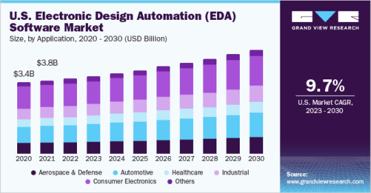
Electronic Design Automation Software Market Growth & Trends
The global electronic design automation software market size is anticipated to reach USD 22.21 billion by 2030, expanding at a CAGR of 9.1% from 2023 to 2030, according to a new study by Grand View Research Inc. The growing usage of advanced electronic components across different areas of healthcare, automotive, and consumer electronic sectors is driving Electronic Design Automation (EDA) software market growth. Apart from this, the proliferation of the Internet of Things (IoT) and connected devices further promotes EDA software market advancement.
Miniaturization of devices and chips is expected to create lucrative opportunities for EDA software. This software assists chipmakers in lowering the errors in Integrated Circuit (IC) and chips, thereby driving the electronic design automation software industry growth. The exponential growth of the integrated circuits market is driving the need for electronic design automation software. The software is increasingly being adopted for designing electronic systems such as printed circuit boards and integrated circuits, supporting the growth of the EDA market.
Furthermore, developments in technology, growing digitization, growth of the electronics manufacturing industry, and increasing adoption of advanced rendering & simulation tools by hardware designers are expected to positively influence the electronic design automation software industry growth over the forecast period. Furthermore, the increasing acceptance and awareness of smart fitness devices are factors enabling electronic design companies to invest in innovative design software tools for designing enhanced & compact products, thereby propelling the EDA software market growth over the forecast period.
Growing demand for EDA software is encouraging various market players to adopt various business strategies to achieve higher profitability in the market for electronic design automation software. Market players are unveiling new solutions by partnering with technology providers to improve their brand identity, propelling the EDA software market growth. For instance, in January 2022, Altium LLC announced a partnership with MacroFab, Inc., a U.S.-based cloud platform provider for electronic production, to launch “Altimade.” The new solution combines elastic manufacturing capabilities and real-time supply chain data, available on the Altium 365 electronic design platform. Altimade empowers customers to request instant quotes and place orders for manufacturing their PCB assembly without exiting the design environment.
Request a free sample copy or view report summary: https://www.grandviewresearch.com/industry-analysis/electronic-design-automation-eda-software-market
Electronic Design Automation Software Market Report Highlights
The services segment is expected to register a CAGR of 10.6% from 2023 to 2030. The segment growth can be attributed to the increasing proclivity of OEMs to outsource their design needs. Furthermore, electronic circuit boards are in high demand in the industry due to their increasing importance in a variety of vital electronic products such as mobile phones and tablets
The cloud segment is expected to register a CAGR of 10.8% from 2023 to 2030. Cloud-based deployment allows for faster distribution, less maintenance, lower costs, and more scalability
The healthcare segment is expected to register a CAGR of 11.5% from 2023 to 2030. The segment growth can be attributed to the benefits of EDA software in healthcare, such as lower costs, improved patient outcomes, faster design & development, enabled regulatory compliance of medical devices, and simulation and testing of medical equipment
The microprocessors & controllers segment is expected to register a CAGR of 9.5% from 2023 to 2030. The increased use of microprocessors in consumer devices such as smartphones, personal computers (PCs), and laptops is expected to drive global demand for the segment
Asia Pacific is anticipated to emerge as the fastest-growing region over the forecast period at a CAGR of 9.6%. A surge in demand for electronic devices together with the prevalence of key electronic component manufacturers in Greater China is expected to drive regional growth
Electronic Design Automation Software Market Segmentation
Grand View Research has segmented the global electronic design automation software market based on product, deployment, application, end-use, and region:
Electronic Design Automation (EDA) Software Product Outlook (Revenue, USD Billion, 2018 - 2030)
Computer-aided Engineering (CAE)
IC Physical Design and Verification
Printed Circuit Board and Multi-chip Module (PCB and MCM)
Semiconductor Intellectual Property (SIP)
Services
Electronic Design Automation (EDA) Software Deployment Outlook (Revenue, USD Billion, 2018 - 2030)
Cloud
On-premise
Electronic Design Automation (EDA) Software Application Outlook (Revenue, USD Billion, 2018 - 2030)
Aerospace and Defense
Automotive
Healthcare
Industrial
Consumer Electronics
Others
Electronic Design Automation (EDA) Software End-use Outlook (Revenue, USD Billion, 2018 - 2030)
Microprocessors & Controllers
Memory Management Unit (MMU)
Others
Electronic Design Automation (EDA) Software Regional Outlook (Revenue, USD Billion, 2018 - 2030)
North America
Europe
Asia Pacific
Latin America
Middle East & Africa
List of Key Players in the Electronic Design Automation Software Market
Advanced Micro Devices, Inc.
Aldec, Inc.
Altair Engineering Inc.
Altium LLC
Autodesk, Inc.
ANSYS, Inc.
Cadence Design Systems, Inc.
eInfochips
EMA Design Automation, Inc.
Keysight Technologies
Microsemi
Synopsys, Inc.
Silvaco, Inc.
The MathWorks, Inc.
Vennsa Technologies
Zuken
Browse Full Report: https://www.grandviewresearch.com/industry-analysis/electronic-design-automation-eda-software-market
#Electronic Design Automation Software Market#Electronic Design Automation Software Market Size#Electronic Design Automation Software Market Share
0 notes
Text
How Are Ethernet ICs Now?

Ethernet ICs are vital components in the electronic components industry, enabling data communication and network connectivity.
In recent years, the market shipments of Ethernet ICs have witnessed continuous growth. According to data, the global market size of Ethernet ICs has been steadily expanding, driven by their widespread adoption in the fields of computers, communications, and industry.
Some well-known Ethernet IC manufacturers include Intel, Broadcom, Cisco, Renesas Electronics, and Texas Instruments. These companies possess extensive expertise and advanced product portfolios in the field of Ethernet technology, constantly driving industry development and innovation.
0 notes
Text
Exploring BGA Assembly: The Key to High-Performance Electronics
Ball Grid Array (BGA) assembly has become a critical technology in the manufacturing of modern electronic devices, offering superior performance and reliability compared to traditional packaging methods. As electronic devices continue to shrink in size while increasing in complexity, BGA has emerged as the go-to solution for mounting integrated circuits (ICs) on printed circuit boards (PCBs). This article delves into the principles of BGA assembly, its benefits, the process involved, and why it has become essential in high-performance electronics.

What is BGA Assembly?
Ball Grid Array (BGA) is a type of surface-mount packaging used for mounting integrated circuits (ICs) onto PCBs. Unlike conventional packages that use leads or pins to make connections, BGA packages use a grid of small solder balls on the underside of the IC, which directly connect to corresponding pads on the PCB. The solder balls are typically made of a tin-lead or lead-free alloy and are arranged in a grid pattern. When the package is placed on the PCB and heated, the solder balls melt, creating a strong electrical and mechanical connection.
BGA assembly is favored for its ability to handle high-density packaging, improve thermal performance, and increase reliability. With the rapid growth of mobile devices, computers, and other high-performance electronics, BGA has become the preferred choice for many manufacturers.
The BGA Assembly Process
The BGA assembly process involves several crucial steps, from PCB preparation to final testing. Here’s an overview of the typical BGA assembly process:
1. PCB Preparation
Before the BGA component can be placed on the PCB, the board needs to be prepared. This step includes cleaning the board to remove any dirt or contaminants that could interfere with soldering. Next, a layer of solder paste is applied to the PCB pads that will correspond with the BGA’s solder balls. The solder paste is typically applied using a stencil to ensure precision.
2. Component Placement
In this step, the BGA component is aligned and placed onto the PCB. This is typically done using automated pick-and-place machines, which use precision robotics to pick up the BGA package and place it onto the PCB pads covered with solder paste. Unlike other surface-mount packages, the BGA package has no leads sticking out, making placement easier and more precise.
Due to the high number of solder balls in a typical BGA package, accurate placement is essential to avoid misalignment, which can lead to poor electrical connections and device failure.
3. Reflow Soldering
Once the BGA component is placed on the PCB, the assembly enters the reflow soldering phase. The entire PCB is heated in a reflow oven, where the temperature gradually rises until the solder paste melts, creating a strong bond between the BGA balls and the PCB pads. After the solder melts, it solidifies as the PCB cools, forming a reliable connection between the BGA and the board.
Reflow soldering is particularly advantageous in BGA assembly because it allows the solder balls to melt simultaneously, ensuring uniform solder joints around the entire package. This process eliminates the risk of cold or dry solder joints, which can result in electrical failures.
4. Inspection and Testing
After reflow soldering, the PCB undergoes inspection to ensure that the BGA has been properly soldered and that there are no defects in the connections. One of the key challenges in BGA assembly is ensuring the quality of solder joints, which are hidden under the package and not visible for visual inspection.
To address this, manufacturers use specialized inspection techniques:
X-Ray Inspection: X-ray imaging is commonly used to inspect the hidden solder joints beneath the BGA package. This allows for the detection of issues such as solder bridges, voids, or incomplete joints that could affect performance.
Automated Optical Inspection (AOI): While AOI is effective for inspecting surface-mounted components, it cannot directly inspect BGA solder joints. However, it is still useful for checking the placement of components and overall board quality.
Electrical Testing: Functional or in-circuit testing is conducted to verify that the BGA connections are electrically sound and the assembled PCB functions as expected.
5. Final Assembly and Packaging
Once the BGA component has passed inspection and testing, the PCB is integrated into its final assembly. This may involve attaching the PCB to other components, encasing it in a protective housing, or connecting it to a power supply or other systems. The finished product is then packaged for shipment or further distribution.
Advantages of BGA Assembly
BGA assembly offers several advantages, which explain why it is increasingly used in high-performance electronics manufacturing:
1. Higher Density and Compactness
One of the key benefits of BGA assembly is its ability to accommodate a high number of connections in a relatively small space. The grid of solder balls enables dense packaging, which allows more components to fit on the PCB without sacrificing size. This is crucial in devices like smartphones and laptops, where space is limited but performance needs are high.
2. Improved Electrical Performance
The BGA package’s direct connection between the chip and the PCB, using the solder balls as conductive paths, reduces the electrical resistance and improves signal integrity. This leads to faster, more reliable signal transmission, making BGA ideal for high-speed circuits and data-intensive applications.
3. Superior Thermal Performance
BGA packages also offer superior heat dissipation compared to traditional packages with leads or pins. The grid of solder balls allows for better heat distribution across the PCB, which is especially important for high-power or high-performance devices that generate a significant amount of heat.
4. Greater Reliability
BGA connections are more robust than traditional leaded packages because the solder balls provide multiple contact points, reducing the risk of mechanical failure. This is especially important in applications where durability and long-term reliability are critical, such as automotive, aerospace, and industrial devices.
5. Smaller Footprint
BGA assemblies have a much smaller footprint than other packaging types, such as leaded packages or chip-on-board (COB) configurations. The reduced size allows for more efficient use of PCB real estate and contributes to the overall compactness of modern devices.
Challenges of BGA Assembly
Despite its many benefits, BGA assembly does come with its own set of challenges:
Inspection and Testing: As mentioned, BGA solder joints are hidden under the component, making it difficult to visually inspect the connections. While X-ray inspection can address this issue, it is expensive and adds to the overall manufacturing cost.
Placement Accuracy: BGA components have a high number of solder balls, and precise placement is essential for creating reliable connections. Misalignment can result in poor performance or failure, which requires meticulous control during the assembly process.
Conclusion
BGA assembly plays a pivotal role in the development of high-performance, compact, and reliable electronic devices. By offering advantages in terms of density, electrical performance, thermal management, and reliability, BGA has become a staple in industries ranging from consumer electronics to automotive and medical technology. Despite challenges related to inspection and placement, advances in automation and inspection technologies continue to enhance the BGA assembly process, ensuring that it remains a cornerstone of modern electronics manufacturing. As technology continues to evolve, BGA assembly will likely remain a key enabler of the increasingly complex and compact devices that define our digital world.
0 notes
Text
Complete Guide to Modern SMT Assembly Line Components and Maintenance
In today's rapidly evolving electronics manufacturing landscape, maintaining an efficient Surface Mount Technology (SMT) assembly line is crucial for producing high-quality printed circuit boards (PCBs). This comprehensive guide explores essential components and maintenance practices that keep your production running smoothly and efficiently.
Understanding Core SMT Assembly Line Components
Pick and Place Machines: The Heart of SMT Assembly
Modern pick and place machines form the cornerstone of any SMT assembly line. These sophisticated machines precisely position components onto PCBs at high speeds. Different manufacturers offer various models to suit different production needs, from high-volume manufacturing to prototype development.
High-speed placement machines come equipped with advanced features like automatic component recognition, vision systems for accurate placement, and flexible feeding systems. These machines can handle components ranging from tiny 0201 packages to larger ICs and connectors.
Feeding Systems: Ensuring Continuous Production
Reliable component feeding systems are essential for maintaining consistent production flow. Modern feeders have evolved significantly, offering features like:
Quick-change mechanisms for rapid product changeover
Smart recognition systems for error prevention
Vibration-free operation for stable component delivery
Enhanced tape handling capabilities for various component sizes
When selecting feeders, compatibility with your pick and place machine is crucial. Regular maintenance of feeders helps prevent common issues like misfeeds or component jams.
Nozzle Systems and Component Handling
Nozzle selection and maintenance significantly impact placement accuracy and speed. Different component types require specific nozzle designs for optimal handling. Modern nozzle systems feature:
Quick-change capabilities for reduced downtime
Self-cleaning mechanisms
Wear-resistant materials
Precise vacuum control
Essential Maintenance Practices
Daily Maintenance Routines
Implementing consistent daily maintenance procedures is crucial for optimal performance:
Visual inspection of critical components
Cleaning of nozzles and feeding systems
Checking vacuum levels and air pressure
Verifying placement accuracy
Inspecting conveyor belt condition
Weekly Maintenance Tasks
More thorough maintenance should be performed weekly:
Deep cleaning of feeding systems
Comprehensive nozzle inspection and cleaning
Checking and adjusting belt tensions
Calibrating placement heads
Inspecting and cleaning vacuum generators
Monthly Preventive Maintenance
Monthly maintenance helps prevent major issues:
Complete system calibration
Thorough inspection of all mechanical components
Lubrication of moving parts
Software updates and backup
Comprehensive accuracy testing
Optimizing Assembly Line Performance
Production Line Integration
Modern SMT assembly lines require seamless integration between components. Consider these factors:
Compatible communication protocols between machines
Synchronized conveyor systems
Integrated quality control systems
Efficient component replenishment systems
Quality Control Measures
Implementing robust quality control measures ensures consistent output:
Regular verification of placement accuracy
Component alignment checks
Solder paste inspection
Post-placement inspection
Temperature profile monitoring
Troubleshooting Common Issues
Component Placement Problems
Address common placement issues through:
Regular calibration of placement heads
Proper nozzle selection and maintenance
Optimal feeder setup and alignment
Regular vision system calibration
Feeder-Related Issues
Prevent feeding problems by:
Regular cleaning and maintenance
Proper tape tension adjustment
Correct splicing techniques
Monitoring wear on critical components
Future-Proofing Your Assembly Line
Upgrading Considerations
Stay competitive by considering these upgrade factors:
Production volume requirements
Component size handling capabilities
Placement speed and accuracy needs
Integration with Industry 4.0 technologies
Training and Documentation
Maintain operational excellence through:
Regular operator training programs
Detailed maintenance documentation
Standard operating procedures
Troubleshooting guides
Conclusion
A well-maintained SMT assembly line is crucial for consistent, high-quality PCB production. By following proper maintenance procedures and understanding your equipment's needs, you can maximize efficiency and minimize downtime. Regular updates to both equipment and procedures ensure your assembly line remains competitive in the ever-evolving electronics manufacturing industry.
Remember that successful SMT assembly operation requires a balance of quality equipment, proper maintenance, and well-trained staff. Investing in these areas will pay dividends in improved productivity and reduced operational issues.
0 notes
Text
Top Electronic Components Manufacturers in India | Powered by Semikart
India has emerged as a significant hub for electronic components manufacturing, driven by the rapid growth of the electronics industry and the government’s initiatives such as ‘Make in India’ and ‘Digital India.’ Electronic components form the backbone of innovation and technology from consumer electronics to industrial equipment. This article highlights India’s top electronic components manufacturers and how Semikart simplifies sourcing these components.
1. Bharat Electronics Limited (BEL)
India’s government owns Bharat Electronics Limited (BEL), a company that specializes in military electronics. For example, it makes parts for radar systems, transmission gear, and semiconductor devices. Based on its reputation for dependability and innovation, BEL serves a wide range of military and civilian uses.
2. Havells India Limited
There is a well-known brand name for electrical and computer parts called Havells. It makes switches, capacitors, and other important parts that are used in a lot of consumer and commercial electronics. Businesses choose Havells because it focuses on quality and new ideas.
3. Kaynes Technology
In India, Kaynes Technology is one of the best companies for Electronic Manufacturing Services (EMS). Kaynes works with companies in the automotive, healthcare, and telecommunications industries because they are good at developing and making custom electronic parts.
4. Continental Device India Ltd. (CDIL)
For making semiconductors, CDIL is one of India’s oldest companies. Customers in industries like automobile, industrial, and consumer electronics buy transistors, diodes, and integrated circuits (ICs). These CDIL goods are famous for being of the highest quality and lasting a long time.
5. SPEL Semiconductor
SPEL Semiconductor was one of the first companies to package and test semiconductors. Integrated circuits and other parts used in advanced technology are made by this company. Because it cares about the environment and making sure its products are accurate, it is a major player in the business.
6. Molex India
Customers love Molex India’s connectors and interconnect options. In fields like healthcare, telecom, and automobiles, Molex is a reliable partner for businesses looking for high-performance electronic parts.
7. Vishay Components India
Passive electrical parts like resistors, capacitors, and inductors are what Vishay Components India does best. It can be used for many things, from home technology to factory automation.
How Semikart Simplifies Electronic Component Sourcing
Semikart connects producers with customers. It is India’s biggest online market for electronic parts. This is how Semikart makes your sources better:
Wide Range of Products: Semikart offers an extensive inventory of components from India’s top manufacturers, ensuring you find everything you need in one place.
Easy Online Access: With a user-friendly platform, Semikart allows businesses and individuals to browse, compare, and purchase components effortlessly.
Competitive Pricing: Semikart direct partnerships with manufacturers ensure competitive pricing and access to genuine products.
Technical Support: The platform provides expert guidance and support to help you choose the right components for your projects.
Fast Delivery: With a robust supply chain network, Semikart ensures timely delivery across India.
Conclusion
An interesting mix of well-known companies and new, innovative ones is helping India’s electronic components business grow. Their high-quality products are shaping the future of technology at companies like Bharat technology Limited, Havells, and Kaynes Technology. The easy way to get these parts is to work with Semikart. This lets you focus on growth and new ideas. Use Semikart to find the best companies in India that make electrical parts for your projects and make sure they work well and reliably.
#semikart#components#electronic parts distributor#buy online electronics components#electronic components distributor#best electronics components#electroniccomponents#electronics
0 notes
Text
Understanding the Physical Design Flow: A Step-by-Step Guide

The design and development of Very Large Scale Integration (VLSI) circuits are pivotal in creating the chips that power today’s electronics. While logical design defines what a chip does, the physical design flow ensures that the chip is manufacturable and performs efficiently. This blog provides an in-depth look at the key steps in the physical design flow of VLSI and its importance in the semiconductor industry.
What is Physical Design in VLSI?
Physical design in VLSI refers to the process of converting a chip’s logical design into a physical layout that can be manufactured on a silicon wafer. It involves placing and routing electronic components and ensuring that the design meets performance, area, power, and manufacturability constraints.
The physical design flow can be broadly categorized into six key stages:
Partitioning
Floorplanning
Placement
Clock Tree Synthesis (CTS)
Routing
Sign-off and Verification
Let’s explore each stage in detail.
1. Partitioning
Partitioning divides the large design into smaller, manageable blocks. This step is crucial for hierarchical designs where sub-blocks are developed and optimized independently. Proper partitioning ensures that communication between blocks is efficient and manageable during later stages of the design.
2. Floorplanning
Floorplanning involves defining the size and shape of the chip and the arrangement of the blocks within it. Key activities during floorplanning include:
Defining Power Planning: Establishing power grids to ensure robust power delivery to all components.
Area Estimation: Estimating the total area required by blocks and interconnections.
Placement of Macro Cells: Positioning large components, such as memory and I/O blocks, to optimize performance and connectivity.
3. Placement
Placement determines the exact locations of standard cells within the chip’s floorplan. The primary goals of placement are:
Minimizing wirelength to reduce signal delay and power consumption.
Ensuring that cells are placed without overlap and that there is enough space for routing.
Optimizing timing constraints to meet performance goals.
4. Clock Tree Synthesis (CTS)
Clock Tree Synthesis ensures that the clock signal reaches all parts of the chip with minimal skew and latency. Key aspects of CTS include:
Clock Buffer Insertion: Adding buffers to balance delays.
Minimizing Skew: Ensuring that the clock arrives at all registers simultaneously.
Optimizing Power Consumption: Reducing dynamic power used by the clock distribution network.
5. Routing
Routing involves establishing physical connections between the placed cells using metal layers. The routing process is divided into two main stages:
Global Routing: Identifies approximate paths for interconnections while avoiding congestion.
Detailed Routing: Creates precise connections between pins and ensures adherence to design rules (DRC).
Challenges during routing include:
Ensuring signal integrity by minimizing crosstalk and electromagnetic interference.
Managing design-rule violations and congestion in dense layouts.
6. Sign-off and Verification
Before manufacturing, the design undergoes rigorous verification to ensure it meets all specifications. This includes:
Timing Analysis: Ensuring the design meets setup and hold time constraints.
Power Analysis: Verifying that power consumption is within acceptable limits.
Design Rule Check (DRC): Ensuring compliance with manufacturing constraints.
Layout vs. Schematic (LVS): Checking that the layout matches the original schematic design.
Once the design passes all sign-off checks, it is sent for tape-out, the final step before manufacturing.
Tools Used in Physical Design
Several Electronic Design Automation (EDA) tools assist in the physical design flow, including:
Synopsys: IC Compiler, PrimeTime
Cadence: Innovus, Tempus
Mentor Graphics: Calibre for DRC and LVS
These tools automate many aspects of the design process, ensuring high efficiency and accuracy.
Challenges in Physical Design
Scaling with Technology Nodes: As feature sizes shrink, managing power, performance, and area (PPA) becomes increasingly complex.
Thermal Management: Ensuring effective heat dissipation in densely packed chips.
Signal Integrity: Maintaining robust communication between components in high-speed designs.
Design Rule Violations: Resolving issues caused by stringent manufacturing constraints.
Conclusion
The physical design flow in VLSI bridges the gap between logical design and chip fabrication, ensuring that designs are optimized for performance, power, and manufacturability. As technology evolves, innovations in physical design methodologies and tools will continue to drive advancements in semiconductor technology. Understanding the intricacies of this process is crucial for engineers aspiring to excel in the semiconductor industry.
#Best Physical Design Service companies in Bengaluru#Top Most Physical Design Service companies in Hyderabad#Most Famous Physical Design Service companies in India#Popular Physical Design Service companies in USA
0 notes
Text
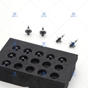
Materials Used in the Manufacturing of IC Sockets for Inspection
Summary
By selecting the right materials, manufacturers can ensure that their IC sockets are not only durable and reliable but also capable of supporting the cutting-edge technologies of tomorrow. As new materials and innovations continue to emerge, the future of IC socket manufacturing promises even greater efficiency and performance for testing and inspection applications.
Introduction
Integrated Circuit (IC) sockets are vital components in the electronics industry, enabling quick and easy testing and inspection of ICs. These sockets facilitate the evaluation of the functionality and performance of ICs without the need to permanently attach them to a circuit board.
The materials used to manufacture these sockets are crucial for their durability, functionality, and reliability during testing. In recent years, semiconductor packages like BGA and QFP have become more compact.
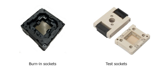
Importance of Material Selection for IC Sockets
The materials used for IC sockets must meet several key requirements to ensure reliable performance during inspection:
Thermal Resistance: IC sockets must be able to withstand high temperatures as they are often subjected to heat during testing. This is especially important when dealing with ICs that operate at elevated temperatures or undergo thermal cycling during the inspection process.
Mechanical Strength: The materials must be robust enough to handle the mechanical stresses of frequent insertion and removal of ICs. This includes maintaining their structural integrity over repeated usage.
Electrical Insulation: As IC sockets often handle high-frequency signals, the materials must be excellent electrical insulators to prevent unintended electrical conduction or short circuits.
Dimensional Stability: The socket must retain its precise shape and alignment even after repeated exposure to heat and mechanical stresses. Any deformation could result in poor connectivity and unreliable testing results.
Machinability: The material must be easy to machine into precise socket designs that accommodate different types of ICs, from simple through-hole packages to more complex BGA sockets (Ball Grid Array) and LGA sockets (Land Grid Array).
Common Materials Used in IC Socket Manufacturing
Several materials are commonly used in the production of IC sockets, each offering specific advantages suited for inspection and testing applications. Below are the most widely used materials:
1. Engineering Plastics
Engineering plastics are among the most common materials used for IC sockets, particularly for high-performance applications. These materials offer a good balance of thermal stability, mechanical strength, and electrical insulation properties.
Polyetheretherketone (PEEK): PEEK is a high-performance thermoplastic known for its excellent thermal resistance, mechanical strength, and chemical stability. It can withstand temperatures up to 250°C, making it ideal for high-temperature inspection applications. PEEK is often used in high-reliability sectors, such as aerospace and semiconductor testing.
Polyetherimide (PEI): PEI is another engineering plastic widely used for IC sockets. It has strong dimensional stability and is capable of withstanding moderate to high temperatures (up to 170°C). PEI is also known for its electrical insulation properties, making it a preferred choice for sockets used in testing ICs with high-frequency signals.
Polyimide (PI): Polyimide is renowned for its exceptional thermal stability, withstanding temperatures as high as 300°C without significant degradation. It is commonly used in advanced testing scenarios, where both high thermal performance and excellent electrical properties are required.
2. Ceramic-Filled Composites
Ceramic-filled composites are often chosen for their enhanced thermal conductivity and dimensional stability. These materials combine the benefits of polymers with ceramic fillers, offering improved mechanical properties and the ability to handle heat better than standard engineering plastics.
3. Metals and Metal Alloys
While the body of the IC socket is generally made from plastics or composites, metal contacts are essential for ensuring good electrical conductivity. These metal components are typically used in the pins or contact areas of the socket.
Beryllium Copper: This alloy is widely used for socket contacts due to its excellent electrical conductivity, high strength, and good corrosion resistance. Beryllium copper allows for the creation of thin, resilient contact points that maintain reliable electrical connections over time.
Phosphor Bronze: Phosphor bronze is another metal alloy used for contact pins. It is known for its durability and ability to retain spring-like properties, ensuring proper engagement with the IC leads.
Read the full article to know more about icsockets
0 notes