#HDI improvement
Explore tagged Tumblr posts
Visit Tumblr Blog
Explore Tumblr blogs with no restrictions, modern design and the best experience.
Last Seen Tumblr Blogs


Fun Fact
Tumblr has a low social media market share in South America.
Note
!!! Recently did a research assignment (annotated bibliography) about research into CDD's so I saw this blog and thought it would be a good place to share!
My topic was originally meant to be recent research into OSDD- but since there's so little research specifically on OSDD, most of the sources I found studied CDDs in general, and it was just that OSDD was included in the sample.
It was a fairly small annotated bibliography so I only had to find 3 sources- but they were all interesting to read. Since I already had to look through them for the assignment I'll provide a brief overview of each one to hopefully make combing through it easier on you.
First One: https://doi.org/10.1708/3814.37993
This one was a case study, aiming to find if a specific type of therapy referred to as schema therapy (which the meaning of is defined in the text as a form of therapy that focuses on improving early maladaptive schemas-- or frameworks for how a person sees things-- by replacing maladaptive coping mechanisms with adaptive ones) is an effective method for treating CDDs. The patient being studied was a 38 year old man with OSDD, as well as PTSD and BPD. He went to therapy once a week for 60 minute sessions with 2 therapists present. To measure how effective the therapy was, he took a questionnaire to measure symptoms before and after treatment. There's no definite conclusion due to limitations of the study such as the fact that CDD patients often have inconsistent results in things like questionnaires- but the study did show an improvement of the scores for symptoms, and a decrease in time spent in therapy in comparison to other methods, indicating it may be useful for treatment for CDDs.
Second One: https://doi.org/10.1080/20008198.2021.1976954
This study focused on seeing if there is a correlation of symptoms of anhedonia- a condition where the person loses the ability to feel pleasure- such as negative affect interference (negative emotions/thoughts interfering with ability to feel positive emotions) and hedonic deficits (deficits in ability to feel pleasure), with the symptoms of dissociation and identity alteration that come with CDD's. The study took a sample of 25 patients in an inpatient program with CDD's and divided them into 4 groups to take questionnaires. They took multiple questionnaires to measure various symptoms, including the HDIS (Hedonic Deficit & Interference Scale), IDQ (International Trauma Questionnaire), and DSO (Disturbances in Self-Organization). From the results they found a moderate to strong correlation between negative affect interference and symptoms in PTSD, with the correlation being higher than in patients with PTSD that didn't have CDD's. However they didn't found a correlation between negative affect interference and hedonic deficits, indicating further need for study on that in patients with CDD's.
Third One: https://doi.org/10.1080/20008198.2022.2031592
This study looked at the link between emotional dysregulation, self injury, and dissociative symptoms, as well as the severity of emotional dysregulation and dissociation in those that have recent history of self injury. The study took a sample of 235 patients with DID, DDNOS, and OSDD- it also lists out other groupings in the patients and the amounts, indicating that the majority groups in the sample were white, women, and had DID. The patients took the DERS (Difficulty in Emotional Regulation Scale) to measure emotional dysregulation, the Dissociative Experiences Scale-II to measure dissociative symptoms, and data from their records was taken for information on history of self injury. A high correlation between the three was found, with 68% of patients having a history of self injury, and 44% having self injured within the past 6 months. Those with recent history of self injury also showed higher levels of emotional dysregulation and dissociative symptoms.
Hope this is an interesting read for you (and anyone else who sees this) as well! It's rather long, but I personally think it's all rather interesting to read into.
Congratulations on your annotated bibliography! I know those are a lot of work, and we really appreciate the dedication and love that goes into each and every one 🫶🫶🫶 Seeing as you linked 3 studies, we'll make 3 different posts for them, all of which will have this ask linked and your account tagged.
If you turned your AnBi in for a grade, we hope you do well 💝💝 We'll get started on these as soon as we can!
Thank you so much for this submission!!
7 notes
·
View notes
Text

Men have grown twice as much as women over past century, study shows (Ian Sample, The Guardian, Jan 22 2025)
"Analysis of records from dozens of countries found that for every 0.2 point increase in HDI, women were on average 1.7cm taller and 2.7kg heavier, while men were 4cm taller and 6.5kg heavier.
This suggests that as living conditions improve, both height and weight increase, but more than twice as fast in men than women.
To see whether similar trends played out within countries, the researchers delved into historical height records in the UK where HDI rose from 0.8 in 1900 to 0.94 in 2022.
During the first half of the century, average female height increased 1.9% from 159cm to 162cm, while average male height rose 4% from 170cm to 177cm.
“To put this in perspective, about one in four women born in 1905 was taller than the average man born in 1905, but this dropped to about one in eight women for those born in 1958,” Halsey said.
Writing in Biology Letters in a study titled “The sexy and formidable male body: men’s height and weight are condition-dependent, sexually selected traits”, the scientists speculate that women’s sexual preferences may have fuelled a trend for taller, more muscular men – although in an age of obesity, heavy does not necessarily mean muscular. (…)
The findings build on previous work that found women want taller men more than men want shorter women.
But there are downsides to being tall. While taller people tend to earn more, they are also more prone to various cancers, possibly because they have more cells that can accumulate mutations which culminate in the disease.
Michael Wilson, professor of ecology, evolution and behaviour at the University of Minnesota, said the faster increase in male height and weight was “striking”.
He said it was consistent with a long-standing idea that females are “the more ecologically constrained” sex because of the demands of reproduction, particularly in mammals where pregnancy and nursing are “energetically expensive”.
“Investment in greater body size by males appears to be sensitive to nutritional conditions,” he said.
“When men grow up with more energy-dense food, they grow bigger bodies, to a greater extent than women."
7 notes
·
View notes
Note
And now that we have discussed GDP, lets address the remaining points I made:
HDI is a slightly better indicator, but the US is also only on the 21st place regardless, behind Canada, Belgium, the United Kingdom and Denmark.
The US has the worlds strongest military. Yes, this is true. But would China or Russia be a better country if they had a stronger one?
If we look at the crime rates, the US is at 89 out of 147 countries, beaten by Morocco, Italy, Vietnam, Kazakhstan and Moldova.
The only thing the US is really the best at (if we don't count the military) is its economy, which is still ranked first globally. But I don't know how that's good for any citizen when their standard of living isn't benefiting from it.
Our HDI is good yes now it could be better. I think if we had better socialist policies that could help people when they do reach poverty or homelessness that would help tremendously. I believe each of those policies should be implemented by the states because that state would know their situation the best.
Neither Russia nor China would be better if their military was stronger because they are corrupt powers and have communist and oligarch interests. Which use their military to benefit themselves unlike America which has used their military to benefit others (Nato)
Our crime is a direct influence of the culture. In my part of the country there is minimal crime and murders so to speak. Now if we were to jump down to El Paso and San Diego we will see a different story as those cities are influenced by the crime of the cartel. Furthermore big American cities have gang cultures which perpetuate crime and violence. But crime is also a response to poverty as people resort to desperation to survive.
The economy plugs back into every American citizens life. The more money that is put into the economy instead of the government is usually money that will improve their lives by the products they consume or their business they’re employed by becomes more successful. Leading to more money into every Americans pocket.
6 notes
·
View notes
Text

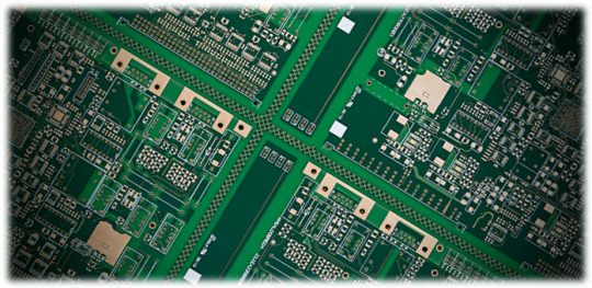
What affects PCB Lead Time
When working with PCB suppliers, you may wonder why some orders take longer than expected. Here’s a clear breakdown of the main factors affecting delivery schedules — based on real industry experience.
1. Design Complexity & Engineering Time • Multilayer PCBs (especially 8+ layers), HDI designs, and impedance control require longer engineering time. • Unclear documentation or last-minute design changes can cause 1–2 day delays.
2. Material & Supply Chain Risks • Fluctuations in copper foil, special base materials, and IC chip availability can extend procurement time. • Global component shortages may prolong lead times by 30%–50%.
3. Manufacturing Process & Quality Control • Special processes such as via-in-pad, heavy copper, or castellated holes require separate scheduling and add time. • Lack of First Article Inspection (FAI) increases the chance of rework, causing 2–3 days of additional delay.
4. Production Issues & External Disruptions • High-difficulty boards like HDI may require re-fabrication in case of defects. • Logistics constraints, regulations (e.g. environmental restrictions), and unexpected events (e.g. quarantines) can also impact delivery.
5. Order Volume & Capacity Allocation • Large orders often need batch processing, while small-volume jobs may be prioritized. • Limited production capacity or poor scheduling can lead to extended delivery times.
✅ How to Improve Delivery Reliability: • Finalize design and engineering requirements early • Maintain safety stock for critical materials • Ensure thorough production testing and reporting • Align expectations and timelines in contracts • Start with trial orders before scaling up
Looking for a trusted PCB manufacturing partner? Hitech is the leading manufacturer in China. We provide professional, on-time delivery from prototyping to mass production. Send us your design files for a quick, competitive quote--we’re ready to support your PCB project.
0 notes
Text
GDP or HDI - how to measure a nation’s development?
Economic development and human well-being are often assessed using two major indicators: Gross Domestic Product (GDP) and the Human Development Index (HDI). GDP, widely used as a benchmark for economic growth, measures the total monetary value of all goods and services produced within the national territory in a given time period. Whereas, Human Development Index (HDI) measures development more holistically and includes dimensions of health, education and income, thereby providing a more rounded perspective on human well-being and overall quality of life.


While GDP reflects economic productivity, HDI includes social factors that contribute to human well-being. For example, countries with high GDP may not have high HDI if wealth is unequally distributed or if healthcare and education services are underdeveloped.
To illustrate the above, given below is a table comparing GDP and HDI of selected countries: United States, Germany, Brazil, India, and Nigeria. These countries represent a range of income levels and development standards.

World Bank. “World Development Indicators: GDP and GDP per capita.” Accessed 2023. https://data.worldbank.org. United Nations Development Programme. “Human Development Index (HDI) Data Center.” Accessed 2023. https://hdr.undp.org/data-center/human development-index.
Key Takeaways:
United States - has a high GDP and is one of the world’s leading economies, yet it ranks lower in HDI compared to countries with similar economic output. Issues like income inequality, limited healthcare access, and high living costs contribute to its lower HDI rank. This means that high GDP does not guarantee high quality of life as social services and equitable income distribution are essential.
Germany - demonstrates balanced development with both high GDP and HDI. Its comprehensive social welfare programs, universal healthcare and quality education contribute to a high HDI. Germany’s HDI ranking illustrates that strong economic policies combined with social welfare result in higher quality of life.
Brazil - is an example of an emerging economy where GDP growth does not fully translate to high HDI. While Brazil has made significant progress, it faces challenges in reducing income inequality, improving public health, and enhancing education access. This implies that economic growth in emerging economies does not always lead to immediate improvements in HDI.
India - has a growing GDP that reflects in its rising economic power, but its HDI remains low due to challenges in healthcare, education and uneven distribution income. Rapid urbanization has also created issues such as pollution and housing shortages.
Nigeria - has low GDP and HDI. These are attributed to factors like political instability, low income levels, limited access to healthcare and education. Despite being an oil-rich country, the benefits of this wealth are not evenly distributed, affecting human development.
Conclusion:
Combined use of GDP and HDI is essential for understanding true development in a nation. This balanced approach allows governments to design policies that foster both economic and social progress, ensuring improved quality of life for all citizens. Only when both GDP and HDI are focal points, will the economy experience sustainable development.
1 note
·
View note
Text
Thin Double Sided FPC Market: Key Players, Competitive Analysis, 2025-2032

MARKET INSIGHTS
The global Thin Double Sided FPC market size was valued at US$ 2.73 billion in 2024 and is projected to reach US$ 4.78 billion by 2032, at a CAGR of 8.6% during the forecast period 2025-2032. While the U.S. market accounted for 28% of global revenue in 2024, China is expected to witness the fastest growth with a projected CAGR of 7.9% through 2032.
A thin double-sided flexible printed circuit (FPC) is a specialized circuit board that combines enhanced flexibility with double-sided micro-wiring capabilities through an ultra-thin substrate (typically under 0.1mm thickness). These advanced PCBs reduce mechanical stress and bias force while maintaining high-density interconnects, making them ideal for compact electronic devices. Key material variations include gold-plated (accounting for 42% market share) and copper-plated (38% share) configurations, each offering distinct conductivity and durability characteristics.
The market growth is primarily driven by expanding applications in consumer electronics (58% of 2024 demand), particularly smartphones and wearables requiring lightweight, bendable circuitry. Furthermore, automotive electrification trends are creating new opportunities, with FPCs increasingly used in advanced driver-assistance systems (ADAS) and in-vehicle infotainment. Recent technological developments include Nitto Denko’s 2023 launch of a 25μm ultra-thin FPC with improved heat resistance, addressing growing thermal management requirements in 5G devices. Market leaders Nippon Mektron and Sumitomo Electric continue to dominate, collectively holding over 35% of global production capacity.
MARKET DYNAMICS
MARKET DRIVERS
Proliferation of Consumer Electronics to Spur Demand for Thin Double-Sided FPCs
The consumer electronics industry remains the largest end-user of thin double-sided flexible printed circuits (FPCs), accounting for over 60% of global demand. This dominance stems from the technology’s ability to enable miniaturization while maintaining reliability in smartphones, wearables, and tablets. With smartphone shipments projected to reach 1.2 billion units annually by 2025, manufacturers increasingly adopt thin double-sided FPCs for their space-saving advantages in high-density interconnect (HDI) designs. These circuits allow for complex multilayer routing in constrained spaces – a critical requirement as device thickness continues to decrease while functionality expands. Recent innovations in gold-plated FPCs offer enhanced signal integrity, further driving adoption in premium consumer devices. The trend towards foldable displays has created additional demand, with FPCs enabling the necessary flexible connections between hinge components.
Automotive Electrification and ADAS Adoption Accelerates Market Growth
Automotive applications represent the fastest-growing segment for thin double-sided FPCs, with demand escalating at nearly 15% CAGR. This surge correlates directly with the automotive industry’s rapid transition to electric vehicles (EVs) and advanced driver-assistance systems (ADAS). Modern vehicles now incorporate over 100 FPCs on average, handling everything from infotainment systems to battery management. The thin double-sided variant proves particularly valuable in EVs where weight reduction is paramount – these circuits can be up to 70% lighter than traditional wiring harnesses while offering superior vibration resistance. Autonomous driving systems further compound demand, requiring high-reliability interconnects for sensors and cameras that must withstand harsh automotive environments. Major manufacturers have responded by developing automotive-grade FPCs with enhanced thermal and chemical resistance, opening new avenues for market expansion.
➤ Leading automotive suppliers have begun incorporating double-sided FPCs in battery monitoring systems, where their thin profile allows integration between cells while monitoring voltage and temperature with minimal space consumption.
MARKET RESTRAINTS
High Manufacturing Costs Limit Adoption in Price-Sensitive Markets
Despite their advantages, thin double-sided FPCs face significant adoption barriers due to production costs that can be 40-60% higher than single-sided alternatives. The sophisticated manufacturing process requires specialized equipment for precise laminating of ultra-thin substrates, along with advanced plating techniques to ensure reliability. This cost premium makes the technology less accessible for budget-oriented applications, particularly in developing markets where price sensitivity remains high. While material innovations continue to drive costs down, the gap remains substantial enough to limit market penetration in mid-range consumer products and industrial applications where cost often outweighs performance benefits.
Technical Challenges in High-Frequency Applications Hinder Wider Implementation
As electronic systems push toward higher frequencies to support 5G and millimeter-wave applications, thin double-sided FPCs face signal integrity challenges. The very thin dielectric layers that enable flexibility can lead to increased crosstalk and insertion losses at frequencies above 10GHz. This poses particular difficulties for RF applications in telecommunications infrastructure and advanced radar systems. While manufacturers have developed specialized materials with low dielectric loss tangents, these premium solutions come at substantially higher costs. The industry continues to grapple with balancing electrical performance, mechanical flexibility, and economic feasibility in next-generation applications.
MARKET OPPORTUNITIES
Medical Electronics Emerges as High-Growth Vertical for Thin Double-Sided FPCs
The medical device sector presents substantial untapped potential, with the global medical electronics market projected to exceed $80 billion by 2027. Thin double-sided FPCs are increasingly specified for implantable devices and wearable medical monitors where flexibility and reliability are paramount. Applications range from cochlear implants to continuous glucose monitors, where the technology’s biocompatibility and fatigue resistance offer distinct advantages. Recent regulatory approvals for novel medical wearables have accelerated development cycles, prompting manufacturers to develop medically-certified FPC solutions with enhanced durability and sterilization compatibility. The trend toward minimally invasive surgical tools also creates demand for ultra-thin FPCs that can navigate tight anatomical spaces while maintaining signal integrity.
Roll-to-Roll Manufacturing Breakthroughs Promise Cost Reductions
Emerging roll-to-roll (R2R) production techniques could significantly lower thin double-sided FPC manufacturing costs while improving yield rates. Current batch processing methods limit throughput and contribute to material waste, but continuous R2R approaches demonstrate potential for 30-40% cost reductions at scale. Several industry leaders have made substantial R&D investments in this area, with pilot production lines already demonstrating promising results for consumer applications. Successful commercialization of these methods could dramatically improve the economic viability of thin double-sided FPCs, potentially opening new application areas in IoT devices and smart packaging where cost has previously been prohibitive.
MARKET CHALLENGES
Supply Chain Vulnerabilities Impact Material Availability
The thin double-sided FPC market faces ongoing supply chain challenges, particularly for specialized polyimide substrates and high-performance adhesives. Over 70% of polyimide production remains concentrated in a limited number of facilities, creating bottlenecks during periods of high demand. Recent geopolitical tensions have exacerbated these issues, with trade restrictions affecting material flows between key manufacturing regions. Manufacturers must navigate extended lead times while maintaining inventory buffers – an expensive proposition given the high material costs. The situation has prompted some producers to explore alternative substrate materials, though these alternatives often require extensive qualification processes that delay time-to-market.
Technical Workforce Shortage Constrains Production Scaling
Industry expansion faces significant headwinds from a global shortage of skilled technicians capable of operating advanced FPC manufacturing equipment. The specialized nature of thin double-sided FPC production requires extensive training in precision lamination, laser drilling, and micro-via plating processes. As veteran operators retire, manufacturers struggle to fill positions, with some reporting vacancy rates exceeding 20% for critical technical roles. This skills gap has forced companies to invest heavily in training programs while simultaneously slowing capacity expansion plans. The challenge is particularly acute in established manufacturing hubs where competition for skilled labor is most intense.
THIN DOUBLE SIDED FPC MARKET TRENDS
Rising Demand for Compact Consumer Electronics to Drive Market Growth
The global thin double-sided FPC market is experiencing robust growth, primarily driven by exponential demand for lightweight and compact consumer electronics. Smartphones, wearables, and foldable devices require high-density, flexible circuits to accommodate advanced functionalities while maintaining slim form factors. The consumer electronics segment currently accounts for approximately 52% of total market revenue, with projections indicating sustained growth at a CAGR of 8.4% through 2035. Furthermore, the miniaturization trend in IoT devices and portable medical equipment continues to accelerate adoption of these ultra-thin circuit boards.
Other Trends
Automotive Electronics Modernization
The automotive sector is witnessing a paradigm shift in electronic architecture, with thin double-sided FPCs becoming critical enablers for next-generation vehicle designs. Modern vehicles now incorporate over 70 electronic control units on average, each requiring reliable connectivity solutions. Flexible printed circuits provide the necessary durability to withstand vibration and thermal stresses in automotive environments. Market analysts project the automotive electronics segment to grow at 9.7% annually through 2030, fueled by increasing autonomous driving capabilities and electric vehicle production.
Material Innovation and Manufacturing Advancements
Material science breakthroughs are significantly enhancing the performance characteristics of thin double-sided FPCs. Recent developments in polyimide substrates with improved thermal conductivity (up to 2.5 W/mK) allow for better heat dissipation in high-power applications. Meanwhile, advanced plating techniques now enable copper trace thicknesses below 10μm while maintaining excellent conductivity. Manufacturing innovations such as roll-to-roll processing have increased production efficiency by 28% compared to traditional batch methods, contributing to cost reductions across the supply chain.
Geographic Market Expansion
Asia-Pacific continues to dominate the thin double-sided FPC market, representing about 63% of global production capacity. While China maintains leadership in volume manufacturing, Southeast Asian countries are emerging as competitive alternatives due to lower operational costs. North America and Europe are experiencing above-average growth rates (7.9% and 6.8% respectively) driven by demand for specialized aerospace and defense applications, where reliability and performance outweigh cost considerations.
COMPETITIVE LANDSCAPE
Key Industry Players
Market Leaders Leverage Innovation and Strategic Partnerships to Maintain Dominance
The global thin double-sided FPC market features a moderately consolidated competitive landscape dominated by major Asian manufacturers, with Nitto Denko and Nippon Mektron collectively holding approximately 25% market share in 2024. These established players benefit from decades of experience in flexible circuit technology, vertically integrated manufacturing capabilities, and strong relationships with electronics OEMs.
While Japanese firms traditionally led this space, Korean and Chinese competitors like Sumitomo Electric and MFS Technology are rapidly gaining traction through aggressive pricing strategies and expanding production capacities. This shift reflects broader supply chain realignments as global electronics brands diversify their supplier base.
Recent industry developments show established players are responding to competitive pressures by: – Investing in advanced roll-to-roll manufacturing technologies for higher yields – Developing thinner substrates (below 25μm) for next-gen wearables and foldables – Expanding application-specific product lines for automotive and medical markets
Meanwhile, emerging Chinese manufacturers such as Shenzhen Baolifeng Electronic and JiangXi Redboard Technology are disrupting traditional value chains through localized production and shorter lead times, particularly for domestic smartphone makers.
List of Key Thin Double Sided FPC Manufacturers
Nitto Denko (Japan)
Nippon Mektron (Japan)
Sumitomo Electric (Japan)
DK-Daleba (South Korea)
Oki Electric Cable (Japan)
TATSUTA Electric Wire and Cable (Japan)
Meiko Electronics (Japan)
NOK Corporation (Japan)
Qdos (Singapore)
MFS Technology (Singapore)
Uniflex Technology (China)
Best Technology Co (China)
Shenzhen Meidear (China)
3G Technology Co (China)
DSBJ (China)
Segment Analysis:
By Type
Gold Plated Segment Leads Due to Superior Conductivity and Durability in High-Frequency Applications
The market is segmented based on type into:
Gold Plated
Subtypes: Electroplated Gold, Immersion Gold
Copper Plated
Subtypes: Rolled Annealed Copper, Electrodeposited Copper
Others
By Application
Consumer Electronics Segment Dominates Due to Rising Demand for Compact, Flexible Circuit Solutions
The market is segmented based on application into:
Consumer Electronics
Subtypes: Smartphones, Wearables, Tablets
Aerospace
Automotive Electronics
Others
By End-User
OEMs Segment Holds Significant Share Due to Direct Integration in Final Products
The market is segmented based on end-user into:
Original Equipment Manufacturers (OEMs)
Contract Manufacturers
Aftermarket Suppliers
Regional Analysis: Thin Double Sided FPC Market
North America The North American thin double-sided FPC market is driven by strong demand from the consumer electronics and aerospace sectors, particularly in the U.S., which accounts for the largest regional market share. Major manufacturers such as Nitto Denko and Sumitomo Electric have a strong presence here, leveraging advanced manufacturing technologies. The region benefits from high R&D investments—approximately $35 billion annually in semiconductor and electronics research—which fosters innovation in flexible circuitry. However, stringent environmental regulations and rising raw material costs pose challenges for suppliers. Nonetheless, the expansion of 5G and IoT applications continues to fuel demand for high-performance FPCs in smart devices and automotive electronics.
Europe Europe’s market is characterized by a focus on precision and sustainability, with key players like DK-Daleba and Meiko Electronics leading the adoption of eco-friendly manufacturing processes. The EU’s Circular Economy Action Plan has accelerated the shift toward recyclable materials in FPC production, particularly in Germany and France. The automotive electronics segment dominates due to the region’s emphasis on electric vehicles (EVs), where thin double-sided FPCs are critical for battery management systems. However, slower growth in consumer electronics and reliance on imports from Asia create supply chain vulnerabilities. Collaboration between academic institutions and manufacturers is helping bridge this gap through localized R&D initiatives.
Asia-Pacific As the largest and fastest-growing market, the Asia-Pacific region, led by China, Japan, and South Korea, accounts for over 65% of global FPC production. China’s market alone is projected to reach $2.8 billion by 2030, fueled by massive electronics manufacturing hubs and government subsidies for domestic players like Nippon Mektron and MFS Technology. The consumer electronics boom—driven by smartphones, wearables, and foldable devices—is the primary growth driver. However, intense price competition and overcapacity in low-tier FPCs have pressured margins. Southeast Asian nations like Vietnam and Thailand are emerging as alternative manufacturing bases, offering cost advantages and tax incentives for foreign investors.
South America South America remains a niche market, with Brazil as the primary adopter of thin double-sided FPCs for automotive and industrial applications. The region’s growth is hindered by economic instability, limited local expertise, and reliance on imported FPCs—particularly from China and the U.S. However, rising FDI in Brazil’s automotive sector, coupled with increasing demand for aftermarket electronics, presents opportunities. Local suppliers like DSBJ are partnering with global manufacturers to improve technical capabilities, though scaling remains slow due to infrastructure bottlenecks and currency fluctuations. The lack of standardized regulations further complicates market entry for foreign players.
Middle East & Africa This region shows long-term potential but limited current traction, with demand concentrated in Israel, Turkey, and the UAE. The automotive and aerospace sectors are the key adopters, though volumes are modest compared to other regions. JHDPCB and Shenzhen Baolifeng Electronic have begun supplying FPCs for defense and telecommunications projects, leveraging partnerships with local distributors. Challenges include high import dependency, underdeveloped supply chains, and low consumer electronics penetration. However, ongoing smart city initiatives—particularly in Saudi Arabia’s NEOM project—are expected to drive incremental demand for advanced FPCs in IoT and renewable energy applications.
Report Scope
This market research report provides a comprehensive analysis of the Global and regional Thin Double Sided FPC (Flexible Printed Circuit) markets, covering the forecast period 2025–2032. It offers detailed insights into market dynamics, technological advancements, competitive landscape, and key trends shaping the industry.
Key focus areas of the report include:
Market Size & Forecast: Historical data and future projections for revenue, unit shipments, and market value across major regions and segments. The Global Thin Double Sided FPC market was valued at USD million in 2024 and is projected to reach USD million by 2032, growing at a CAGR of % during the forecast period.
Segmentation Analysis: Detailed breakdown by product type (Gold Plated, Copper Plated, Others), application (Consumer Electronics, Aerospace, Automotive Electronics, Others), and end-user industry to identify high-growth segments and investment opportunities.
Regional Outlook: Insights into market performance across North America, Europe, Asia-Pacific, Latin America, and the Middle East & Africa, including country-level analysis. The U.S. market size is estimated at USD million in 2024, while China is projected to reach USD million by 2032.
Competitive Landscape: Profiles of leading market participants including Nitto Denko, Nippon Mektron, Sumitomo Electric, DK-Daleba, and others, covering their product offerings, R&D focus, manufacturing capacity, and recent developments.
Technology Trends & Innovation: Assessment of emerging technologies in flexible circuit manufacturing, material advancements, and evolving industry standards for thin double-sided FPCs.
Market Drivers & Restraints: Evaluation of factors driving market growth along with challenges, supply chain constraints, regulatory issues, and market-entry barriers.
Stakeholder Analysis: Insights for component suppliers, OEMs, system integrators, investors, and policymakers regarding the evolving ecosystem and strategic opportunities in the FPC market.
Related Reports:https://semiconductorblogs21.blogspot.com/2025/06/fieldbus-distributors-market-size-and.htmlhttps://semiconductorblogs21.blogspot.com/2025/06/consumer-electronics-printed-circuit.htmlhttps://semiconductorblogs21.blogspot.com/2025/06/metal-alloy-current-sensing-resistor.htmlhttps://semiconductorblogs21.blogspot.com/2025/06/modular-hall-effect-sensors-market.htmlhttps://semiconductorblogs21.blogspot.com/2025/06/integrated-optic-chip-for-gyroscope.htmlhttps://semiconductorblogs21.blogspot.com/2025/06/industrial-pulsed-fiber-laser-market.htmlhttps://semiconductorblogs21.blogspot.com/2025/06/unipolar-transistor-market-strategic.htmlhttps://semiconductorblogs21.blogspot.com/2025/06/zener-barrier-market-industry-growth.htmlhttps://semiconductorblogs21.blogspot.com/2025/06/led-shunt-surge-protection-device.htmlhttps://semiconductorblogs21.blogspot.com/2025/06/type-tested-assembly-tta-market.htmlhttps://semiconductorblogs21.blogspot.com/2025/06/traffic-automatic-identification.htmlhttps://semiconductorblogs21.blogspot.com/2025/06/one-time-fuse-market-how-industry.htmlhttps://semiconductorblogs21.blogspot.com/2025/06/pbga-substrate-market-size-share-and.htmlhttps://semiconductorblogs21.blogspot.com/2025/06/nfc-tag-chip-market-growth-potential-of.htmlhttps://semiconductorblogs21.blogspot.com/2025/06/silver-nanosheets-market-objectives-and.html
0 notes
Text
Best China PCB Manufacturer By Cesgate
In the short-evolving electronics enterprise, choosing a dependable PCB dealer is an important choice for groups aiming for innovation and cost-overall performance. One of the most famous alternatives globally is a China PCB Manufacturer, the country’s strong manufacturing infrastructure, aggressive pricing, and technological enhancements. Whether you're a startup or a massive agency, sourcing your posted circuit boards from China can provide awesome blessings.
Why Choose a China PCB Manufacturer?
There are numerous compelling motives why groups global favor to paintings with a China PCB Manufacturer. First and fundamental is fee-effectiveness. China's big commercial scale permits for lower production expenses, which translates to better pricing for clients. Additionally, many manufacturers in China provide prototyping and mass manufacturing services, giving businesses flexibility at particular stages of product improvement.
Another key benefit is the price of producing. A PCB Manufacturer commonly has the capability to supply quick-turn PCBs interior days, even for complex designs. This can notably reduce time-to-marketplace for brand spanking new products, this is important in pretty competitive industries like customer electronics, vehicle, and clinical devices.
Quality and Technological Advancements
While low fee is a vital detail, it doesn’t come at the rate of first-rate. Leading PCB manufacturers are ISO certified and study worldwide requirements collectively with RoHS, UL, and IPC. Many of these producers spend money on the present day era, inclusive of superior multilayer PCB fabrication, HDI boards, and flexible PCBs, ensuring they meet worldwide pleasant expectations.
China is likewise on the leading edge of smart production. Automation, AI-pushed first-rate tests, and on-line order tracking systems are absolutely extensive in plenty of facilities. This technique while you select a China PCB Manufacturer, you also are profiting from a streamlined and obvious manufacturing method.
Choosing the Right Partner
With such a whole lot of alternatives to be had, how do you pick the high-quality PCB Manufacturer in China to your venture? Start via assessing their revel in and organization awareness. Some producers focus on automotive PCBs, others in customer electronics or enterprise programs. Checking consumer critiques, certifications, and sample merchandise can also provide precious insights into their reliability.
Communication is some other key factor. An authentic PCB Supplier in China can have a responsive income and assist group that speaks your language, is aware of your requirements, and is capable of offering technical help even as needed.
Conclusion
Partnering with a China PCB Manufacturer can provide your commercial business enterprise an aggressive component thru reduced costs, fast turnaround times, and get entry to remarkable products. However, deciding on the right accomplice calls for careful evaluation. By focusing on super, experience, and communique, you may find out a dependable production companion in China that allows you to supply your digital improvements to lifestyles successfully and fee-successfully.
0 notes
Text
HDI PCBs: The Backbone of Modern Miniaturized Electronics
In today’s fast-paced, technology-driven world, electronic devices are becoming smaller, faster, and more powerful. This evolution demands an equally advanced foundation to support it. That’s where HDI Printed Circuit Boards (HDI PCBs) come in. At Pcb-Togo Electronic, Inc, we specialize in crafting high-quality HDI PCBs that are not only compact but also deliver exceptional performance, reliability, and innovation.
What Are HDI PCBs?
HDI stands for High-Density Interconnect, a type of printed circuit board that offers a higher wiring density per unit area than traditional PCBs. These boards incorporate fine lines and spaces, smaller vias, and capture pads to maximize the efficiency of interconnections. HDI PCBs typically feature blind and buried vias and often utilize via-in-pad technology to further reduce space.
Their compact design and high-layer density make them the ideal choice for electronics where space and weight are at a premium, such as smartphones, tablets, wearable devices, and advanced medical equipment.
Why HDI PCBs Are Essential for Miniaturized Electronics
As electronic products shrink in size, the demand for lightweight, compact circuit boards with more functionality grows exponentially. HDI PCBs fulfill this demand by enabling the integration of more components within smaller footprints without sacrificing performance.
At Pcb-Togo Electronic, Inc, our HDI PCB manufacturing process focuses on precision and quality to ensure that every board can handle the demands of modern electronic devices. With tighter tolerances and enhanced electrical performance, HDI PCBs are engineered to meet the rigorous expectations of the industry’s leading innovators.
Go right here to explore how our HDI PCBs support high-speed signal transmission and minimize signal loss—two vital characteristics for devices where performance is non-negotiable.
Key Benefits of Choosing HDI Printed Circuit Boards
Compact Design
HDI technology allows for reduced board size by utilizing microvias and tighter trace widths. This not only saves valuable space but also helps decrease the overall weight of the end product—an essential factor in mobile and wearable electronics.
Improved Signal Integrity
The advanced layout of HDI PCBs reduces the signal paths, lowering the risk of signal degradation. At Pcb-Togo Electronic, Inc, we incorporate state-of-the-art techniques to maintain signal clarity, making our HDI PCBs ideal for high-frequency applications.
Higher Reliability
Fewer connection points and more direct routing result in enhanced mechanical and electrical performance. HDI PCBs manufactured by us are rigorously tested for durability and function under various stress conditions to ensure long-term reliability.
Faster Transmission
Shorter routing distances and lower cross-talk make HDI PCBs capable of faster signal transmission—vital for devices requiring real-time processing and responsiveness.
Design Flexibility
With multiple build-up layers and more complex stack-ups, designers have greater flexibility in incorporating intricate components. This freedom allows for innovation in product design and performance optimization.
Industries That Rely on HDI PCB Technology
HDI Printed Circuit Boards are not limited to consumer electronics. Their applications span across several high-tech industries, including:
Automotive electronics, where they enable the development of advanced driver assistance systems (ADAS) and infotainment.
Medical devices, such as wearable heart monitors and diagnostic tools that require miniaturized but reliable circuitry.
Aerospace and defense, where every gram and millimeter counts, and reliability is mission-critical.
Industrial automation, which demands robust and compact PCBs to support sensors, controllers, and IoT-enabled machinery.
Why Choose Pcb-Togo Electronic, Inc?
As a trusted manufacturer of HDI Printed Circuit Boards, Pcb-Togo Electronic, Inc combines technical expertise with customer-centric service. From rapid prototyping to large-scale production, we work closely with clients to deliver tailored solutions that align with their product goals.
We understand that time-to-market can be critical, so our streamlined production processes are designed to reduce lead times without compromising on quality. Plus, our engineers are available for technical support throughout the product development cycle.
You can find out more about our services and capabilities by visiting our website or contacting our customer support team directly.
Actionable Steps to Get Started
If you're an OEM, engineer, or product designer looking to upgrade your electronic products, consider the following steps:
Evaluate your current PCB needs – Consider the limitations of your existing designs and where HDI PCBs could enhance performance.
Consult with our experts – At Pcb-Togo Electronic, Inc, we offer free consultations to help you determine the best stack-up and layout strategy.
Request a prototype – Begin your journey with a prototype to validate the design before scaling up production.
Scale confidently – With proven quality assurance protocols, we ensure consistency in every production run.
Find Out More about how our team can help bring your next-generation product to life using cutting-edge HDI PCB technology.
Conclusion
In the world of modern electronics, precision, performance, and miniaturization are non-negotiable. HDI PCBs stand at the forefront of this transformation, and Pcb-Togo Electronic, Inc is proud to be a leader in this space. Our expertise in HDI Printed Circuit Boards ensures that our clients stay ahead of the curve with reliable, high-performance circuit solutions.
Whether you're developing the next smartphone or a critical medical device, partnering with us guarantees you access to the best in HDI technology. Go right here to connect with our experts and start your next innovation journey today.
Original Link: https://pcbtogo.blogspot.com/2025/06/hdi-pcbs-backbone-of-modern.html
0 notes
Text
Electronics Evolution Powers 9.9% CAGR Growth in Global ED Copper Foils Market
Electrodeposited copper foils (ED copper foils) are thin copper layers produced through an electroplating process, whereby an electric current deposits a uniform, ultra-thin copper film onto a conductive substrate. As a foundational component in the electronics industry, ED copper foils are integral to the manufacture of printed circuit boards (PCBs), serving as the conductive foundation for electronic components in devices ranging from smartphones and laptops to industrial controls and automotive electronics.
According to recent analysis, the global ED copper foils market was valued at US$ 9.5 billion in 2022. Fueled by accelerated demand in electronics, miniaturization trends, and burgeoning applications in electric vehicles (EVs) and renewable energy, the market is projected to grow at a compound annual growth rate (CAGR) of 9.9% from 2023 to 2031, reaching US$ 22.2 billion by the end of 2031. This significant expansion underscores the pivotal role of ED copper foils in next-generation technologies and manufacturing processes.
Market Drivers & Trends
Electronics Miniaturization
Ongoing innovations in semiconductor devices, integrated circuits, and electronic components drive the trend toward smaller, lighter, and more compact electronic devices. ED copper foils, with their ability to offer extremely thin, uniform conductive layers, enable designers to pack more circuitry into limited PCB real estate. As consumer electronics continue to shrink and performance demands rise, manufacturers rely on advanced ED copper foils to achieve higher layer counts, finer line widths, and improved signal integrity.
Flexible Electronics & High-Density Interconnect (HDI) Boards
The rise of flexible electronics—used in foldable smartphones, wearable devices, and medical sensors—demands copper foils that can bend without cracking or losing conductivity. ED copper foils, characterized by high ductility and uniform thickness, meet these requirements. Likewise, HDI PCBs, which offer faster signal transmission and greater component density, depend on ultra-thin ED copper foils to form microvias and fine traces.
Electric Vehicle (EV) and Renewable Energy Adoption
As automakers accelerate EV production, ED copper foils find application in battery packs, power electronics modules, and onboard chargers. The superior conductivity, thermal management, and lightweight properties of ED copper foils contribute to battery efficiency and overall vehicle performance. In parallel, renewable energy storage systems—particularly lithium-ion batteries used for solar and wind power—incorporate ED copper foils as current collectors, driving incremental demand in energy sectors.
Advanced Manufacturing Processes
The Modified Semi Additive Process (MSAP) represents a breakthrough in PCB fabrication, enabling finer line widths and reduced material usage. Innovations such as Mitsui’s “MicroThin™” and Circuit Foil’s “DoubleThin” ED copper foils optimize MSAP performance, yielding higher circuit densities and improved reliability. R&D investments by leading manufacturers continually refine deposition technologies, surface treatments, and carrier foil properties to meet evolving PCB fabrication requirements.
Diversification of End-Use Applications
Beyond consumer electronics, ED copper foils serve in automotive electronics (airbag systems, infotainment, advanced driver-assistance systems), aerospace avionics, healthcare instrumentation, and industrial automation. As these sectors increasingly rely on sophisticated PCBs for control, sensing, and communication, the addressable market for ED copper foils expands accordingly.
Latest Market Trends
Thin-Gauge Foil Adoption: Manufacturers now offer ED copper foils with thicknesses as low as 1 µm (micron), catering to next-generation chip-scale packaging and ultra-HD mobile devices. Thinner foils reduce weight, lower material costs, and improve thermal dissipation—all critical for high-performance applications.
Surface Treatment Innovations: Electrochemical surface treatments (e.g., black oxide, micro-roughening) enhance adhesion between copper foil and dielectric substrates. This is especially important for high-frequency and high-pressure laminates used in 5G infrastructure and advanced radar systems.
Eco-Friendly Processing: Environmental regulations and sustainability goals drive the development of greener electroplating chemistries and water-recycling systems. Key players are investing in closed-loop plating baths, waste reduction, and energy-efficient deposition lines to minimize carbon footprints.
Customized Foil Solutions: To address unique customer specifications, suppliers increasingly offer tailored foil properties—such as specific grain orientations, tensile strength levels, and peel strengths—enabling better compatibility with diverse PCB manufacturing processes.
Key Players and Industry Leaders
The global ED copper foils market features a mix of established conglomerates and specialized manufacturers. Major industry participants include:
Oak-Mitsui Technologies LLC
Circuit Foil USA
All Foils, Inc.
Mitsui Kinzoku
Sheldahl Flexible Technologies, Inc.
Arlon
Rogers Corporation
JX Nippon Mining & Metals Corporation
Nitto Denko Corporation
Avocet Precision Metals
CIVEN Metal
Denkai America
Targray Technology International
NAN YA PLASTICS CORPORATION
Others
These players collectively hold a significant market share, continuously investing in research, expanding capacities, and forging strategic partnerships to stay ahead of technological shifts.
Recent Developments
Global Patent License Agreement (April 1, 2020): Circuit Foil Luxembourg and Mitsui Mining & Smelting Co., Ltd. entered a global patent license concerning Mitsui’s MSAP technology. This agreement enables fabricators to use Circuit Foil’s ultra-thin “DoubleThin” copper in MSAP processes, accelerating adoption of finer line HDI PCBs and boosting demand for next-gen ED copper foils.
Capacity Expansions (2023–2024):
Oak-Mitsui Technologies inaugurated a new high-volume plating line in Texas (USA) to support rising EV battery substrate demand.
All Foils, Inc. expanded its Illinois plant with a dedicated R&D pilot line for sub-3 µm foil development, targeting advanced semiconductor packaging.
R&D Collaboration (2024): Arlon partnered with a leading automotive OEM to co-develop copper foil alloys optimized for harsh under-hood environments and high-temperature electrical connectors in EVs.
Strategic Acquisitions (2024): JX Nippon Mining & Metals acquired a minority stake in a Taiwanese ED copper foil startup focused on sustainable plating chemistries, strengthening its foothold in the rapidly growing Asia Pacific market.
Download now to explore primary insights from our Report in this sample - https://www.transparencymarketresearch.com/sample/sample.php?flag=S&rep_id=70767
Market Opportunities
Customized Product Development: As PCB OEMs demand foils with precise mechanical and electrical specifications (e.g., specific peel strengths and grain structures), manufacturers that offer bespoke foil solutions can secure long-term contracts and premium pricing.
Expansion into Emerging Markets: Rapid industrialization and digitalization in Southeast Asia, Latin America, and Eastern Europe open new avenues for ED copper foil supply. Localizing production or forging distribution partnerships in these regions can yield first-mover advantages.
Integration with Renewable Energy Storage: With global renewable energy capacity expected to double by 2030, demand for high-performance Li-ion batteries and energy storage systems will surge. ED copper foils serve as essential current collectors; thus, foil producers partnering with battery manufacturers can tap into multi-billion-dollar opportunities.
Electric Vehicle Supply Chains: As EV penetration accelerates (projected to exceed 30% of new vehicle sales by 2030), copper foil requirements for battery packs, motor windings, and power electronics will escalate. Companies aligning product roadmaps to EV OEM specifications can capture significant share in this specialized segment.
Advanced Packaging & 5G Infrastructure: The rollout of 5G networks and adoption of advanced semiconductor packaging techniques (e.g., chip-scale packaging, fan-out wafer-level packaging) create demand for ultra-thin, high-reliability ED copper foils. Foil suppliers focusing on sub-2 µm thicknesses and enhanced thermal management properties can capitalize on next-generation electronics trends.
Future Outlook
Looking ahead to 2031, the ED copper foils market is poised for sustained double-digit growth, driven by:
Proliferation of 5G-Enabled Devices: With projected global 5G smartphone shipments exceeding 1 billion units by 2026, HDI and multi-layer PCBs will become ubiquitous. ED copper foils enabling high-frequency signal integrity and miniaturized interconnects will see robust demand.
Automotive Electrification & Autonomous Systems: By 2030, EVs may comprise over 50% of new vehicle sales in key markets (e.g., Europe, China, North America). Additionally, advanced driver-assistance systems (ADAS) and in-vehicle infotainment continue to demand sophisticated PCBs. Consequently, ED copper foil usage in batteries, onboard chargers, and complex electronic modules will expand.
Energy Storage & Renewable Integration: As grids evolve to incorporate more intermittent renewable sources, large-scale battery storage projects will drive demand for ED copper foils in energy storage modules. Research into solid-state batteries and next-gen chemistries may further alter foil requirements, favoring high-purity, high-conductivity variants.
Sustainability & Circular Economy Initiatives: Regulatory pressures in North America and Europe focusing on reduced hazardous waste and greenhouse gas emissions—will encourage adoption of eco-friendly plating chemistries and closed-loop water treatment. Suppliers investing in sustainable production processes will gain market differentiation and compliance advantages.
Overall, industry analysts believe that continuous innovation in foil composition, surface treatments, and deposition techniques combined with strategic alignment to end-user requirements—will shape the competitive landscape through 2031. Manufacturers that proactively invest in R&D, scalable production capabilities, and strategic partnerships will be well-positioned to capitalize on the projected US$ 22.2 billion market by 2031.
Market Segmentation
By Form
Rolls
Sheets
By Type
Standard ED Copper
Rolled Copper
Resistive Copper
Others
By Application
Printed Circuit Boards (PCBs
Copper Clad Laminates (CCL
Li-ion Batteries
IC Package Substrates
High-Density Interconnect (HDI) Boards
High-Frequency Circuit Substrates
EMI Shielding
Others
Regions Covered
North America
Latin America
Europe
Asia Pacific
Middle East & Africa
Why Buy This Report?
Comprehensive Market Analysis: Detailed insights into global and regional market dynamics, including cross-segment analysis (form, type, application) and in-depth qualitative assessments (drivers, restraints, opportunities, trends).
Historical & Forecast Data: Quantitative data for 2022 (historical baseline) and a robust forecast through 2031, including market size (US$ billion) and volume (tons).
Competitive Landscape: Company profiles of leading players (e.g., Oak-Mitsui, Circuit Foil, All Foils, Mitsui Kinzoku, Sheldahl, Arlon, Rogers, JX Nippon, Nitto Denko, Avocet, CIVEN, Denkai, Targray, NAN YA), highlighting strategies, financials, product portfolios, and recent developments.
Technological Insights: Coverage of advanced manufacturing processes (MSAP, thin-gauge deposition), surface treatments (black oxide, micro-rough), and sustainable plating technologies.
Future Outlook & Strategic Recommendations: Analyst viewpoints on emerging trends (5G, EVs, renewable integration), along with actionable recommendations for market entry, product development, and M&A opportunities.
Value-Added Resources: Delivered in Electronic (PDF) + Excel formats, including pivot tables, forecasting models, Porter’s Five Forces analysis, value chain assessment, and country-level breakdowns for key markets (U.S., Canada, Germany, U.K., France, Spain, Italy, Russia & CIS, Japan, China, India, ASEAN, Brazil, Mexico, GCC, South Africa).
Explore Latest Research Reports by Transparency Market Research:
Zeolite Membrane Market: https://www.transparencymarketresearch.com/zeolite-membrane-market.html
Bulletproof Glass Market: https://www.transparencymarketresearch.com/bulletproof-glass-market.html
RDX, HMX, and C-4 Market: https://www.transparencymarketresearch.com/rdx-hmx-and-c-4-market.html
Nonwoven Hygiene Materials Market: https://www.transparencymarketresearch.com/nonwoven-hygiene-materials-market.html
About Transparency Market Research Transparency Market Research, a global market research company registered at Wilmington, Delaware, United States, provides custom research and consulting services. Our exclusive blend of quantitative forecasting and trends analysis provides forward-looking insights for thousands of decision makers. Our experienced team of Analysts, Researchers, and Consultants use proprietary data sources and various tools & techniques to gather and analyses information. Our data repository is continuously updated and revised by a team of research experts, so that it always reflects the latest trends and information. With a broad research and analysis capability, Transparency Market Research employs rigorous primary and secondary research techniques in developing distinctive data sets and research material for business reports. Contact: Transparency Market Research Inc. CORPORATE HEADQUARTER DOWNTOWN, 1000 N. West Street, Suite 1200, Wilmington, Delaware 19801 USA Tel: +1-518-618-1030 USA - Canada Toll Free: 866-552-3453 Website: https://www.transparencymarketresearch.com Email: [email protected]
0 notes
Text
Printed Circuit Board Market Future Trends: Emerging Technologies and Growth Opportunities Driving Innovation
The printed circuit board market is witnessing significant transformation as innovation and technological advancements propel its growth. PCBs, the backbone of modern electronic devices, continue to evolve in response to emerging industry needs, consumer demands, and new applications. Understanding the future trends shaping the PCB market is essential for manufacturers, investors, and technology enthusiasts seeking to capitalize on opportunities and anticipate challenges.

One of the foremost trends in the PCB market is the increasing demand for miniaturization. As electronic devices become more compact and multifunctional, the need for smaller, lighter, and more efficient PCBs has intensified. This trend is especially prominent in sectors like consumer electronics, healthcare, and automotive, where space constraints and performance requirements drive innovation. Flexible PCBs and rigid-flex boards are gaining popularity as they allow intricate designs that fit into compact devices without compromising functionality.
Advanced materials are another crucial factor shaping the PCB market’s future. The traditional use of fiberglass and epoxy resins is gradually being supplemented or replaced by high-performance substrates such as polyimide, ceramic, and Teflon. These materials offer superior thermal stability, electrical performance, and mechanical strength, which are critical for high-frequency and high-speed applications. This shift supports the growing demands of 5G technology, aerospace, and military electronics where reliability under extreme conditions is vital.
The rise of 5G technology is a major catalyst driving the evolution of PCBs. The implementation of 5G networks requires PCBs that can handle high-frequency signals with minimal interference and signal loss. This has led to innovations in high-density interconnect (HDI) PCBs, which allow more components to be packed into a smaller area with enhanced electrical performance. The demand for HDI PCBs is expected to surge as 5G infrastructure expands globally, impacting telecommunications, IoT devices, and smart cities.
Sustainability and environmental concerns are increasingly influencing the PCB market’s future. The electronics industry is under pressure to reduce its environmental footprint, leading to the development of eco-friendly PCB manufacturing processes and materials. Lead-free soldering, recyclable substrates, and reduced hazardous chemical use are becoming standard practices. Companies that embrace green manufacturing are likely to gain competitive advantages as consumers and regulators prioritize sustainability.
Automation and Industry 4.0 integration are revolutionizing PCB manufacturing. The adoption of artificial intelligence (AI), robotics, and machine learning in production lines improves precision, reduces defects, and accelerates manufacturing cycles. Automated optical inspection (AOI) systems and real-time monitoring help maintain high-quality standards while reducing costs. This trend not only boosts efficiency but also allows manufacturers to respond swiftly to customized and small-batch orders, which are increasingly common due to diversified product demands.
The automotive industry continues to be a major driver of PCB market growth, especially with the rise of electric vehicles (EVs) and autonomous driving technology. PCBs in EVs must withstand higher temperatures and voltages while maintaining safety and durability. Advanced PCBs facilitate battery management systems, power electronics, and sensor integration crucial for EV performance. Additionally, autonomous vehicles rely heavily on sophisticated sensor arrays and computing power, all of which depend on innovative PCB designs.
Healthcare technology is another promising sector influencing PCB trends. The surge in wearable medical devices, telehealth solutions, and diagnostic equipment requires PCBs that offer reliability, miniaturization, and biocompatibility. Flexible PCBs enable comfortable and accurate wearable sensors, while multilayer PCBs support complex diagnostic devices. The ongoing digitalization of healthcare creates a continuous demand for cutting-edge PCB solutions tailored to medical applications.
Global supply chain dynamics also impact the PCB market’s future. The COVID-19 pandemic exposed vulnerabilities in electronics supply chains, prompting companies to rethink sourcing and manufacturing strategies. There is a noticeable trend toward regionalization and diversification to minimize risks and reduce lead times. This shift may result in increased investments in local PCB manufacturing capabilities, encouraging innovation and customization closer to end markets.
Another important future trend is the increasing use of embedded components within PCBs. Embedding passive and active components directly into the PCB substrate reduces assembly time, improves reliability, and enables higher circuit density. This technology is particularly valuable in compact and high-performance devices such as smartphones, tablets, and aerospace electronics, where every millimeter of space counts.
Lastly, the integration of PCBs with emerging technologies such as augmented reality (AR), virtual reality (VR), and artificial intelligence (AI) will open new growth avenues. These technologies demand highly complex, lightweight, and reliable PCBs to support sensors, processors, and communication modules. As these applications gain traction across entertainment, education, and industrial sectors, PCB manufacturers will need to innovate to meet their unique requirements.
In conclusion, the printed circuit board market is poised for dynamic growth fueled by miniaturization, advanced materials, 5G adoption, sustainability initiatives, and Industry 4.0 automation. Key industries such as automotive, healthcare, and telecommunications will continue to drive demand for innovative PCB solutions. Manufacturers who embrace emerging technologies, invest in eco-friendly processes, and adapt to shifting supply chain models will be best positioned to thrive. As the market evolves, staying informed about these future trends will be essential for all stakeholders navigating the complex landscape of PCB technology.
0 notes
Text
PCB Design Software Market Outlook: Size, Trends & Forecast from 2025 to 2035
The PCB design software market is expected to expand at a high growth rate from 2025 to 2035 with the development of high-end electronics, PCB design automation, and the emergence of AI-based circuit optimization. It is expected to grow from USD 5.35 billion in 2025 to USD 21.91 billion in 2035 at a compound annual growth rate (CAGR) of 15.1% over the forecast period.
Get Sample Report: - https://www.futuremarketinsights.com/reports/sample/rep-gb-854
Global PCB (printed circuit board) design software market has become an essential component of the electronics industry, which strengthens innovation in areas such as consumer electronics, automotive, healthcare, aerospace and telecommunications. Such as devices become more compact, powerful and interconnected, demand for sophisticated PCB layouts and designs has increased rapidly. PCB design enables software engineers and designers to create accurate, functional circuit board layouts, simulate circuit behavior and verify the design parameters before the physical prototype. It not only improves product reliability, but also accelerates time-to-market and reduces growth costs. With the ongoing development of techniques like 5G, IOT, and AI, PCB design tools are more important in helping tool companies maintain a competitive lead.
Key Market Insights
One of the most important trends that shape the PCB design software market is to increase cloud-based solutions. Cloud-competent PCB tools provide many advantages on traditional on-primeses software, such as real-time cooperation, spontaneous updates and access from any device. This change allows design teams worldwide to work efficiently, reduce bottlenecks and increase productivity.
Another major trend design software has an integration of artificial intelligence and machine learning abilities. These characteristics can automate regular functions, detect potential design defects, and adapt to the layout for performance and cost. Since PCBs become more complicated with high-gradation interconnects (HDIs) and the rise of flexible boards, AI-assisted design tools help manage the complexity and improve accuracy.
PCB is also affecting PCB design practices. Designers are focused on rapidly reducing power consumption, reducing physical waste and choosing environmentally friendly components. PCB design software is developing to include characteristics that support these goals, such as thermal analysis, electrical integrity equipment and life cycle assessment.
Challenges and Opportunities
Despite its growth, PCB design software faces many challenges in the market. One of the primary issues is the steep learning state associated with advanced design devices. Many small and medium enterprises (SMEs) struggle with limited technical expertise and resources and adopt and use high-end software. This makes a demand for more spontaneous, user -friendly platforms that do not compromise on performance or functionality.
Rapid changing technology scenario is also a challenge. As new standard and communication protocols emerge, software vendors must continuously update their platforms to remain relevant. Ensuring compatibility with various hardware configurations and developing customers' requirements requires constant innovation and investment.
On the other hand, these challenges create enough opportunities. The increasing demand for consumer electronics and smart devices, especially in emerging markets, is meeting the requirement of efficient PCB design solutions. Educational institutions and training centers are also adopting PCB software for engineering courses by compreheering user Aadhaar. Additionally, software providers are searching for membership-based pricing models to attract cost-conscious customers, allowing more market to enter the market.
Regional Analysis
Geographically, the North America PCB design software holds an important part of the market, inspired by the presence of leading technology firms, strong R&D infrastructure and advanced engineering equipment. The United States, in particular, is a major market focusing on innovation and the high concentration of electronics manufacturing companies.
The Asia-Pacific is expected to see the fastest growth in the forecast period, which is inspired by increasing electronics production in countries such as China, Japan, South Korea and India. Cost benefits of the region, government support for manufacturing, and expanding semiconductor industry makes it a hotband for PCB design activities. Local firms are investing rapidly in advanced design software to increase productivity and product quality.
Europe also plays an important role in the market, especially in areas such as motor vehicle, industrial equipment and healthcare. Countries such as Germany, UK and France are known for engineering excellence and are adopting a fast digital design equipment to streamline product development processes. Meanwhile, the Middle East, Africa and Latin America are experiencing gradual development, with the possibility of industrial digitization and development of infrastructure.
Competitive Outlook
PCB design software market is highly competitive, strive to separate themselves through product innovation, customer service and strategic partnership with mixed players and emerging vendors. Companies are focusing on offering end-to-end solutions that cover planned capture, layout design, signal integrity analysis and manufacturing documentation. Integration with other devices in the product development life cycle, such as mechanical CAD and simulation software, is becoming increasingly important to offer an innate design experience.
The merger and acquisition is a common strategy among market leaders to expand their portfolio and enter new markets. Open-source platforms and startups are also creating waves by offering hobbies, cost-effective options for educational users and small enterprises.
Explore In-Depth Analysis-Click Here to Access the Report:- https://www.futuremarketinsights.com/reports/pcb-design-software-market
List of Top PCB Design Software Companies
Altium Limited
Cadence Design Systems
Siemens EDA (Mentor Graphics)
Autodesk Inc.
Keysight Technologies
Zuken Inc.
Ansys Inc
DipTrace
Proteus Design Suite (Labcenter Electronics)
Eagle (Autodesk)
Segmentation Outlook
By Component:
By component, the market includes PCB design software, PCB layout, schematic capture, and PCB design services, which are further segmented into designing services and support & maintenance.
By Deployment:
By deployment, the market is categorized into on-premise PCB design software and cloud-based PCB design software.
By Application:
By application, the market covers IT & computing, consumer electronics, telecommunications, healthcare, automotive, defense & military, and others.
About Future Market Insights (FMI)
Future Market Insights, Inc. (ESOMAR certified, recipient of the Stevie Award, and a member of the Greater New York Chamber of Commerce) offers profound insights into the driving factors that are boosting demand in the market. FMI stands as the leading global provider of market intelligence, advisory services, consulting, and events for the Packaging, Food and Beverage, Consumer Technology, Healthcare, Industrial, and Chemicals markets. With a vast team of over 400 analystsworldwide, FMI provides global, regional, and local expertise on diverse domains and industry trends across more than 110 countries.
Contact Us:
Future Market Insights Inc. Christiana Corporate, 200 Continental Drive, Suite 401, Newark, Delaware – 19713, USA T: +1-347-918-3531 For Sales Enquiries: [email protected] Website: https://www.futuremarketinsights.com LinkedIn| Twitter| Blogs | YouTube
0 notes
Text
How to Choose the Right PCB Manufacturer for Your Project
When you're developing a new electronic product, one of the most critical decisions you'll make is selecting a printed circuit board (PCB) manufacturer. A high-quality PCB is the backbone of any electronic device, and a reliable manufacturer ensures your designs are brought to life with precision, durability, and performance in mind. But with so many options available, how do you know which one is right for your needs?
In this guide, we’ll walk through the key factors to consider when choosing a PCB partner, what makes a manufacturer stand out, and how to avoid common pitfalls. Whether you're a startup working on a prototype or an established company moving into mass production, this article will help you make an informed decision.
Why Your Choice of PCB Manufacturer Matters
The PCB is not just another component—it’s the heart of your device. Poor-quality boards can lead to product failures, delays in production, and costly revisions. On the other hand, working with the right manufacturer can improve your product’s reliability, speed up development cycles, and even reduce costs.
This is why many professionals in the electronics space invest time in researching and partnering with trusted printed circuit board manufacturers who have a proven track record.
Key Factors to Consider When Choosing a PCB Manufacturer
1. Experience and Specialization
Not all PCB manufacturers are created equal. Some focus on low-volume prototyping, while others are geared toward high-volume production. Depending on your project, you should look for a manufacturer that aligns with your specific needs.
For example, if you're designing complex multi-layer boards, make sure the manufacturer has extensive experience in producing such designs. A company that regularly handles high-frequency or HDI (High-Density Interconnect) boards will be more equipped to handle advanced requirements.
2. Quality Standards and Certifications
Quality assurance is essential in PCB manufacturing. Look for certifications such as ISO 9001, UL listing, or IPC standards compliance. These certifications indicate that the manufacturer follows recognized best practices and quality control protocols.
Ask if they conduct Electrical Testing (E-Test), X-ray inspection, and other reliability tests. A manufacturer that prioritizes quality will always have robust systems in place to ensure each board meets the required specifications.
3. Production Capabilities
It’s crucial to understand the scope of what your manufacturer can offer. Can they handle the board sizes, layer counts, and materials your design requires? What about turnaround times for prototyping or mass production?
A good manufacturer will offer a clear breakdown of their capabilities, including:
Minimum and maximum board sizes
Supported layer counts
Material types (e.g., FR4, Rogers, etc.)
Surface finish options (e.g., HASL, ENIG, OSP)
Lead time flexibility
Having this information upfront helps you determine if the manufacturer can scale with your project’s needs.
4. Customer Support and Communication
Your relationship with a PCB manufacturer should feel like a partnership. Responsive communication and good customer support are essential, especially if issues arise during production.
Choose a company that provides clear, timely responses and is open to discussing your technical concerns. Ideally, you’ll work with a team that’s invested in helping you succeed—not just one that processes orders and moves on.
5. Pricing Transparency
Cost is always a factor, but the cheapest option isn't always the best. Look for manufacturers that provide detailed quotes, including breakdowns of tooling, materials, testing, and shipping. This ensures there are no surprises later.
You should also understand their pricing model—some manufacturers offer better rates for bulk orders, while others specialize in fast-turn prototypes at a premium.
Domestic vs. Overseas Manufacturers
A common question in the selection process is whether to go with a domestic or overseas manufacturer.
Domestic manufacturers often offer faster shipping, better communication, and easier quality control. They may cost more upfront, but the reduced risk and faster turnarounds can make up for it in the long run.
Overseas manufacturers, particularly in Asia, tend to offer lower costs. However, language barriers, longer shipping times, and quality control challenges can be drawbacks, especially for time-sensitive or high-precision projects.
That said, many printed circuit board manufacturers based in the U.S. or Europe now offer the best of both worlds—competitive pricing with high-quality standards and excellent customer service.
Red Flags to Watch Out For
Choosing the wrong PCB partner can result in production delays, increased costs, or even complete project failure. Here are some warning signs to watch for:
Lack of certifications or quality assurance processes
Poor or inconsistent communication
No clear information about production capabilities
Hidden fees or vague pricing
Limited reviews or a poor reputation in the industry
Always do your due diligence—read reviews, request samples, and even visit their facilities if possible.
Questions to Ask Before Committing
Here are some questions to ask when evaluating potential PCB partners:
What industries do you typically serve?
Can you share recent case studies or examples of similar projects?
What testing and inspection processes do you use?
What is your typical lead time for prototypes and production runs?
How do you handle design revisions or errors?
Asking these questions upfront helps set expectations and ensures you’re working with a manufacturer that understands your goals.
The Value of Long-Term Partnerships
As your product evolves, having a dependable PCB partner becomes even more valuable. A strong relationship can lead to better pricing, faster response times, and even input on design for manufacturability (DFM). The right printed circuit board manufacturers act not just as suppliers, but as strategic allies in your product development journey.
Final Thoughts
Choosing the right PCB manufacturer can make or break your electronics project. It’s not just about finding someone who can produce your board—it’s about finding a partner who understands your vision, meets your quality expectations, and grows with your business.
Take your time, do your research, and don’t hesitate to reach out to multiple manufacturers before making your decision. When done right, the relationship you build with your PCB manufacturer can be one of the most valuable assets in your entire product development process.
0 notes
Text
U.S. Railing Market: From Classic to Contemporary – Design That Defines
U.S. Railing Industry Overview
The U.S. Railing Market was valued at USD 5.92 billion in 2022. It is projected to expand at a compound annual growth rate (CAGR) of 3.9% from 2023 to 2030. This growth stems from several key factors, including the increasing demand for affordable housing and rising government investments in residential construction.
Additionally, a growing preference for eco-friendly products, driven by heightened environmental concerns, is contributing to the market's expansion. The rapid growth of the U.S. construction industry, fueled by modernization and the ongoing shift of populations from rural to urban areas for better opportunities, also plays a significant role. Furthermore, the U.S. Administration's announced plans for constructing affordable homes in the coming years are expected to further propel the growth of the railing market.
Detailed Segmentation:
Material Insights
The wood railing segment led the market and accounted for the largest revenue share of 41.5% in 2022. The segment is expected to witness growth on account of the excellent aesthetic properties and affordable prices of wood. Due to its high strength, longevity, and ease of maintenance, wood is extensively used in railing applications.
The demand for metal railing is expected to grow at a CAGR of 4.2% throughout the projected period 2023-2030 on account of their high strength and durability. Metal railings are made of stainless steel, aluminum, brass, wrought iron, and cast iron. Metal railings are robust, sturdy, and require minimal maintenance, which, in turn, is expected to lead to the growth of the railing market in the U.S.

Application Insights
The residential application segment accounted for the highest market share of 52.0% in 2022 and is anticipated to grow at a CAGR of 4.1% over the forecast year. The majority of the revenue generated by the residential railing market comes from metal and composite railing. The residential sector has been growing significantly and is predicted to rise considerably throughout the projection period. The growth in single-family residential construction and remodeling activities in the U.S. are mainly driving the residential sector. Therefore, the demand for railing in the U.S. is anticipated to increase with the increase in residential construction and remodeling activities.
The non-residential sector accounted for USD 2,848.1 in 2022, and it is growing at a significant rate over the forecast year. The demand for railing in the non-residential sector of the U.S. is expected to increase due to the rebounding of offices and commercial spaces. In addition, corporate buildings, hotels, retail centers, and industrial structures need railing installed across their properties for security purposes. These elements are expected to encourage the expansion of the non-residential railing market in the U.S.
Gather more insights about the market drivers, restraints, and growth of the U.S. Railing Market
Key Companies & Market Share Insights
The U.S. railing market exhibits high competition owing to the presence of established players in this market with vertical integration across the value chain of railing. Some competitors also focus on increasing their innovations through mergers and acquisitions with top manufacturers in order to gain a competitive edge.
Key participants in the market are also focusing on technological developments for improving the quality of raw materials, components, and installation processes, thus, creating strong competition for new entrants. Additionally, the players are fulfilling the demand for eco-friendly railing systems, and hence their market penetration is higher. Some prominent players in the U.S. railing market include:
Q-railing
VIVA Railing
Century Aluminum Railing
GRECO Architectural Metals
AMERICAN RAILING SYSTEMS, INC.
The Wagner Companies
ViewRail
Fortress Building Products
HDI Railing Systems
Trex Company, Inc.
Barrette Outdoor Living
Order a free sample PDF of the Market Intelligence Study, published by Grand View Research.
0 notes
Text
How Sandpiper Fits is Revolutionizing Industrial Efficiency
In the ever-evolving landscape of industrial engineering, precision and efficiency remain at the core of every breakthrough technology. One such innovation reshaping industries is Sandpiper Fits, a concept that integrates advanced material science with manufacturing processes to optimize performance. Whether applied in automated systems, pneumatic conveying, or specialized mechanical applications, Sandpiper Fits offers enhanced durability, seamless integration, and significant efficiency gains.Get more news about Sandpiper Fits,you can vist our website!
What Makes Sandpiper Fits Stand Out? At its core, Sandpiper Fits represents a fusion of precision engineering and industrial adaptability. It incorporates state-of-the-art components engineered for longevity and optimal performance, making it a preferred choice in demanding applications. By ensuring tighter tolerances and superior compatibility with existing systems, manufacturers can reduce downtime, enhance workflow, and lower maintenance costs.
One of the most compelling aspects of Sandpiper Fits is its role in automation. Industries relying on conveyor systems, fluid dynamics, and pneumatic solutions find immense value in its precision-oriented design. For example, in material handling processes, accurate fits reduce friction, minimizing wear and ensuring prolonged operational efficiency.
Applications Across Industries Sandpiper Fits is particularly relevant in fields such as:
Pneumatic and Liquid Conveying Systems: It helps maintain airtight seals and reduces operational inefficiencies.
Precision Manufacturing: Components designed under the Sandpiper Fits framework adhere to stricter tolerances, improving performance.
Automated Systems: Enhanced compatibility ensures smoother integration in force automation and sales force automation setups.
Given your expertise in industrial processes and automation, Sandpiper Fits aligns well with innovations in HDI PCBs, advanced ceramics, and specialized engineering solutions. Its precision-driven approach complements high-performance materials like boron nitride and ceramic valve cores, which you’ve previously explored in your structured articles.
Future Prospects and Industry Advancements Looking ahead, the continued refinement of Sandpiper Fits technology promises even greater improvements in efficiency and sustainability. With the global industry pushing toward eco-friendly and cost-effective solutions, implementing such precise components will help reduce waste, improve production cycles, and support greener practices.
As industries advance, integrating technologies like Sandpiper Fits into automated systems will become a standard practice rather than an exception. Its ability to streamline processes and enhance productivity ensures that companies adopting it will stay ahead in the competitive landscape.
0 notes
Text
UV Exposure Etching Machine Market Set to Reach $711.7 Million by 2035
The UV Exposure Etching Machine market is projected to grow from $420.5 million in 2024 to $711.7 million by 2035, with a compound annual growth rate (CAGR) of 4.9% over the forecast period. This growth is primarily driven by the rising demand across high-precision applications in semiconductor fabrication, PCBs, MEMS, and integrated optics.
Detailed Analysis - https://datastringconsulting.com/industry-analysis/uv-exposure-etching-machine-market-research-report
Key Applications and Growth Drivers
UV Exposure Etching Machines are instrumental in producing detailed and accurate micro-patterns, essential for:
Semiconductor Fabrication: Ensures precise photolithography for wafer processing.
Printed Circuit Boards (PCBs): Used in high-density interconnect (HDI) boards for modern electronics.
MEMS Production: Enables intricate pattern etching needed for microdevices.
Integrated Optics: Supports the development of photonic integrated circuits for data communication and sensors.
The increasing integration of electronics in consumer devices, automotive systems, and healthcare technology continues to drive market demand. The evolution toward miniaturized, high-performance components further underscores the critical need for advanced UV etching technologies.
Industry Landscape and Competitive Dynamics
The UV Exposure Etching Machine market is characterized by intense competition, with several key players leading innovation and market expansion. Prominent companies include:
Circuit Specialists Inc.
Photo Chemical Systems Inc.
GeSi Equipment Ltd.
Radiant Technologies Inc.
Mycronic AB
Plasma-Therm LLC
Rudolph Technologies Inc.
EV Group
Visitech AS
Technic Inc.
Tokyo Electron Limited
These firms are investing heavily in R&D, automation, and AI-driven etching processes, enabling faster throughput and improved resolution for increasingly complex electronic architectures.
Market Trends and Strategic Opportunities
Several factors are shaping the future trajectory of the market:
Technological Innovation: The shift toward UV nanoimprint lithography and hybrid etching systems is creating performance advantages.
Rising Consumer Electronics Demand: Smartphones, wearables, and IoT devices require high-precision circuitry that UV etching systems deliver.
Industry-Wide Adoption: Beyond electronics, industries such as aerospace, defense, and biomedical engineering are adopting UV exposure etching for advanced microfabrication tasks.
Strategic partnerships and collaborations with OEMs (Original Equipment Manufacturers), alongside the entry into untapped regional markets, present significant opportunities for market players aiming to expand their global footprint.
Regional Trends and Market Expansion
North America and Asia Pacific are the leading regions in terms of adoption and production. The market dynamics in these regions are defined by:
Strong demand from electronics and semiconductor industries
Government incentives supporting high-tech manufacturing
Established supply chains with advanced technology integration
While these mature markets continue to drive core revenues, growth is expected to accelerate in emerging economies such as Brazil, Saudi Arabia, and South Africa. These regions present opportunities for TAM expansion and revenue diversification, as infrastructure investments and industrial automation gain momentum.
Supply Chain Outlook
The supply chain of the UV Exposure Etching Machine market is evolving due to:
Technological Complexity: High-precision systems require advanced component sourcing and testing.
Cost Barriers: Significant capital investment is needed for equipment, R&D, and workforce training.
Global Distribution Strategies: Manufacturers are focusing on optimizing logistics and after-sales support in high-growth regions.
From raw material suppliers and equipment manufacturers to distributors and end users, the ecosystem is undergoing a shift toward integration and agility, driven by the growing demand for lean production methods and rapid deployment.
About DataString Consulting
DataString Consulting provides end-to-end market research and business intelligence services for both B2B and B2C markets. With over 30 years of combined leadership experience, our team specializes in:
Strategic roadmap development
TAM (Total Addressable Market) assessments
Competitive benchmarking
Opportunity mapping
We deliver tailored insights that filter market noise and translate complex data into actionable strategies. With industry specialists monitoring over 15 industries and 60+ sub-sectors, we empower organizations to unlock hidden potential and stay ahead of market trends.
0 notes
Text
Understanding the Differences Between Rigid, Flex, and Rigid-Flex PCBs

Introduction
In the world of electronics manufacturing services, PCBs (Printed Circuit Boards) are a critical component in nearly all electronic devices. From smartphones to medical devices, PCBs are the backbone of modern electronics. However, not all PCBs are created equal. Depending on the application, PCBs can be designed in various forms, such as rigid, flexible, or rigid-flex.
In this blog, we will delve into the differences between rigid, flex, and rigid-flex PCBs, helping you understand which type is best suited for your specific electronics manufacturing services needs.
1. Rigid PCBs: The Standard Choice
Rigid PCBs are the most common type of circuit boards used in electronics today. They are made from a solid, inflexible material such as FR4, which is a composite of fiberglass and resin. Rigid PCBs are typically used in applications where the circuit board will remain stationary and not be exposed to constant bending or flexing.
Key Features of Rigid PCBs:
Sturdy and Durable: Rigid PCBs are highly durable and can handle the demands of many different applications.
Cost-Effective: Due to their widespread use and simple design, rigid PCBs are often the most cost-effective option.
Common Applications: Rigid PCBs are commonly used in consumer electronics, automotive systems, and industrial equipment.
Benefits of Rigid PCBs:
Reliability: Rigid PCBs offer a solid foundation for electronic components, ensuring stable and reliable performance.
Ease of Assembly: The rigid structure makes it easier to assemble and mount electronic components, which is essential for mass production.
2. Flexible PCBs: Ideal for Compact and Portable Devices
Flexible PCBs are designed to be bent, twisted, and shaped to fit into compact or irregularly shaped enclosures. Made from flexible materials like Polyimide (PI) or PET (Polyethylene Terephthalate), flexible PCBs can be folded and flexed without breaking or damaging the circuitry.
Key Features of Flexible PCBs:
Flexibility: Flexible PCBs can bend and conform to different shapes, making them ideal for applications with space constraints.
Lightweight: Flexible PCBs are lightweight, which is important in portable devices.
Thin and Compact: These PCBs are thinner and more compact than rigid PCBs, offering more design flexibility.
Benefits of Flexible PCBs:
Space Efficiency: Flexible PCBs allow for smaller and more compact device designs.
Durability in Challenging Environments: These PCBs can withstand vibrations, shocks, and environmental stresses, making them ideal for wearables and medical devices.
Reduced Wiring: With flexible PCBs, designers can eliminate the need for multiple connectors and wiring, simplifying the design and improving reliability.
3. Rigid-Flex PCBs: A Hybrid Solution for Complex Designs
Rigid-flex PCBs combine the best features of both rigid and flexible PCBs. These PCBs are made by integrating rigid PCB sections with flexible PCB sections. The result is a hybrid design that offers the durability of rigid PCBs with the flexibility of flexible PCBs.
Key Features of Rigid-Flex PCBs:
Hybrid Design: Rigid-flex PCBs consist of both rigid and flexible sections, allowing for more complex and versatile designs.
High-Density Interconnects (HDI): Rigid-flex PCBs are often used in high-density applications where space is limited but performance requirements are high.
Compact and Reliable: The integration of both rigid and flexible components allows for high-density designs without sacrificing durability.
Benefits of Rigid-Flex PCBs:
Design Flexibility: Rigid-flex PCBs allow for intricate and compact designs while maintaining high performance and reliability.
Improved Durability: By combining both rigid and flexible sections, these PCBs are less prone to damage caused by flexing or mechanical stress.
Space Optimization: Rigid-flex PCBs can be folded and bent into tight spaces, making them ideal for applications such as smartphones, tablets, and medical devices.
4. Choosing the Right PCB Type for Your Application
When deciding between rigid, flex, and rigid-flex PCBs, it’s essential to consider your application’s specific requirements. Each type of PCB has its advantages and limitations, making it suitable for different use cases.
When to Choose Rigid PCBs:
If your application involves static electronics where the circuit board will remain stationary.
When cost is a major factor and the design does not require flexibility.
If the application involves consumer electronics, industrial systems, or automotive electronics.
When to Choose Flexible PCBs:
If your application requires compact or portable devices where space is limited.
When flexibility is needed for bending or folding the circuit board to fit into irregularly shaped enclosures.
If the application is in wearables, medical devices, or mobile electronics.
When to Choose Rigid-Flex PCBs:
When your application requires the best of both worlds—rigid sections for stability and flexible sections for space efficiency and durability.
In applications that involve high-density interconnects or complex geometries, such as smartphones, tablets, or advanced medical devices.
When flexibility is needed in some parts of the circuit board but rigidity is required in others.
Conclusion
Choosing the right type of PCB for your project depends on several factors, including size, flexibility, cost, and performance requirements. Whether you need the sturdiness of rigid PCBs, the flexibility of flexible PCBs, or the hybrid benefits of rigid-flex PCBs, each type plays a crucial role in the electronics manufacturing services landscape.
By understanding the differences between rigid, flex, and rigid-flex PCBs, you can make an informed decision about the best solution for your product, ensuring that it meets both design and performance requirements.
Ready to explore high-quality electronics manufacturing services for your PCB manufacturing needs? Reach out to a trusted manufacturer today to ensure reliable and cost-effective solutions.
Also read:
How to Choose the Right Electronics Manufacturing Services Partner for Your Project
Custom PCB Manufacturing for Niche Electronics Applications
Cost-Effective Strategies in Circuit Board Manufacturing Without Compromising Quality
How Global Supply Chain Challenges Are Impacting Circuit Board Manufacturing
#electronics manufacturing#electronics#circuit board manufacturing#pcb manufacturing#electronics manufacturing services
0 notes