#Bypass capacitor
Text

Hey Persia,
Shit's gone to hell, as usual. Managed to limp my ride into some podunk town called Yucca. Found a "mechanic" - and I use that term loosely. Place is called "Yucca Car Repair Shop," but it looks more like a junkyard had a baby with a scrapheap.
This is Mike, the so-called expert. Pendejo looks like he couldn't fix a toaster, let alone my wheels. Problem is, I'm already behind schedule. Got a gig lined up and every minute I waste here is eddies slipping through my fingers.
Been thinkin' about bypassing the coupling and rigging a hotwire. Mike's squawking that it'll fry the compressor, but what the hell does he know? All I need is for this bucket of bolts to make it to Night City. Well, after I knock out this quick cargo run.
Persia, you'd be laughing your ass off if you could see this place. Remember when we used to joke about those "mechanics" who couldn't tell a flux capacitor from their own culo? This guy's their king.
Fuck it. I'm gonna do it my way. If the car explodes, at least it'll be more exciting than this dustbowl. Wish me luck, chica. I'll need it.
Still miss ya,
V
3 notes
·
View notes
Text
EXG Synapse — DIY Neuroscience Kit | HCI/BCI & Robotics for Beginners
Neuphony Synapse has comprehensive biopotential signal compatibility, covering ECG, EEG, EOG, and EMG, ensures a versatile solution for various physiological monitoring applications. It seamlessly pairs with any MCU featuring ADC, expanding compatibility across platforms like Arduino, ESP32, STM32, and more. Enjoy flexibility with an optional bypass of the bandpass filter allowing tailored signal output for diverse analysis.
Technical Specifications:
Input Voltage: 3.3V
Input Impedance: 20⁹ Ω
Compatible Hardware: Any ADC input
Biopotentials: ECG EMG, EOG, or EEG (configurable bandpass) | By default configured for a bandwidth of 1.6Hz to 47Hz and Gain 50
No. of channels: 1
Electrodes: 3
Dimensions: 30.0 x 33.0 mm
Open Source: Hardware
Very Compact and space-utilized EXG Synapse
What’s Inside the Kit?:
We offer three types of packages i.e. Explorer Edition, Innovator Bundle & Pioneer Pro Kit. Based on the package you purchase, you’ll get the following components for your DIY Neuroscience Kit.
EXG Synapse PCB
Medical EXG Sensors
Wet Wipes
Nuprep Gel
Snap Cable
Head Strap
Jumper Cable
Straight Pin Header
Angeled Pin Header
Resistors (1MR, 1.5MR, 1.8MR, 2.1MR)
Capacitors (3nF, 0.1uF, 0.2uF, 0.5uF)
ESP32 (with Micro USB cable)
Dry Sensors
more info:https://neuphony.com/product/exg-synapse/
2 notes
·
View notes
Text
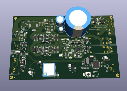
Let me introduce my current main WIP. It's not fandom related, it's for my model railroad, and it's not yet finished.
This is a rendering of a circuit board that I'm designing at the moment. It will be a DCC command station. My model railroad is run digitally, which means the tracks carry digital signals that tell each locomotive and switch individually how to run, which lights to turn and so on. The command station is the device that generates that. I have a number of different layouts, one of which has a good command station, one of which has a crappy old one, and the final one isn't even digital yet. So this will be the one that solves all issues for me, hopefully.
The design above isn't finished yet, and even the parts that are are not yet fully representative. The different capacitors are just there as options; some screen print overlaps; and some components (in particular all plugs and the relays that control the programming track) don't have 3D models so they don't show up.
Planned features:
Four layer board
10-25 V DC output, software controllable
Up to 5A output power, limited mainly by the main switching regulator.
Input 15-25V either AC or DC with polarity protection, selectable with some solder bridges (not yet in there). Optionally you can also bypass the main power regulator with another solder bridge (that I haven't added yet); useful in case you use e.g. a laptop power supply with a switchable voltage and don't need any regulation after that.
Railcom support
USB connection; not yet sure what for, but the main chip I'm using has USB support and I have some spare USB connectors here, so in it goes.
Speaking: The chip is an STM32L433RCT6P, chosen because I found it in stock at an electronics distributor. 64 kB RAM, 256 kB EEPROM, with support for an additional up to 256 MB externally (there's a spot for that on the board) and lots of fun extras that I don't technically need. It has an FPU! I don't need an FPU, but I will definitely do some floating point math computation on it just for fun.
Main external connection is WLAN using an ESP32 WROOM U module. I haven't decided on the housing, but I may go for extruded aluminum, so it's the U version that allows and requires an external antenna
It supports XBUS/XpressNet connections for old throttles from Lenz and Roco that I should probably throw away, but I paid good money for them, dang it.
It supports CAN for LCC / OpenLCB. I may not populate this part on all boards that I'm building, because I haven't actually decided whether I am interested. But the chip has CAN functionality built in, so why not.
There's an I2C connection to connect a cheap tiny OLED display for status messages.
Test points for all important signals (in particular the different internal voltage levels; yes, there is 3.3V, A3.3V and -3.3V and I need all of them).
Stuff still to add:
I will add pin headers (or space for pin headers anyway) for all the remaining pins on the STM32, and perhaps some on the ESP32, for future expansions.
Status LED and stop/go button on the front
Wire it all up, maybe move some stuff (mostly the STM32 around), which will cause all sorts of fun new routing issues.
Adjustments to make the jacks line up with the front panel once I've decided on a housing.
Features I'm not considering adding:
s88. I vaguely know what it is but I don't have any devices like that, and if that ever changed I could probably build (or perhaps buy) a converter that connects them via CAN.
Other buses like LocoNet.
Ethernet. I don't need it and it's actually more expensive than WLAN in this day and age.
In terms of software, I'm planning to use DCC-Ex on it. The whole project actually started out as a DCC-Ex shield, but once I realised that this wouldn't fit, I decided to make it standalone. Now, DCC-Ex is designed for Arduino, not STM32, and it doesn't support XpressNet, nor OpenLCB, nor Railcom, and their Wifi protocol is pretty weird and annoying which will be an issue (I'm planning to write my own control app for iPhone for it), so I'll probably change that or just replace it with the z21 one… so really, the software will not look a lot like DCC-Ex once I'm done with it.
Will this all work? I have honestly no idea. I mean, I'm fairly confident, I'd have given up on this long ago otherwise, but I have no guarantees either way until I've spent a lot of money on components and circuit boards and start soldering. Turns out doing it this way is not really cheaper than just buying a half-way decent one. That's what makes it exciting, though!
If it does work, obviously this will be released as open source. But it's still going to be a few days (more realistically weeks) before it's even ready to order the parts, and then a lot of soldering (current BOM stands at 194 actual components), and then a lot of software development before it's ready for that.
5 notes
·
View notes
Text
I love my ipod mini. I want to do a bypass capacitor mod on it and get a newer battery for it. I already flash modded it with 512GB of storage. I've used these since childhood so rhey have never felt old to me, they just are a thing. This particular one I bought for really cheap, and every part was defective in some way. I'm still giving it all the love I can

3 notes
·
View notes
Text
Principles of anti-interference design for printed circuit boards
Principles of anti-interference design for printed circuit boards
Layout of power cord:
1. According to the current size, try to widen the wire routing as much as possible.
2. The direction of power and ground wires should be consistent with the direction of data transmission.
3. A decoupling capacitor of 10-100 μ F should be connected to the power input terminal of the printed circuit board.
Layout of secondary ground wire:
1. Separate digital from analog.
2. The grounding wire should be thickened as much as possible, and at least 3 times the allowable current on the printed board should be passed, generally up to 2-3mm.
3. The grounding wire should form a dead loop as much as possible, which can reduce the potential difference of the grounding wire.
Three decoupling capacitor configuration:
1. The input end of the printed circuit board power supply is connected to an electrolytic capacitor with a temperature of 10-100 μ F. It would be even better if it could be greater than 100 μ F.
2. A 0.01~0.1 μ F ceramic capacitor is connected across the VCC and GND of each integrated chip. If space does not allow, a 1-10 μ F tantalum capacitor can be configured for every 4-10 chips.
3. Devices with weak anti noise capabilities and large changes in turn off current, as well as ROM and RAM, should have capacitors indirectly decoupled at VCC and GND.
4. Install a 0.01 μ F decoupling capacitor on the reset terminal "RESET" of the microcontroller.
5. The lead wires of decoupling capacitors should not be too long, especially for high-frequency bypass capacitors that cannot have leads.
Four component configuration:
1. The clock input terminals of the clock generator, crystal oscillator, and CPU should be as close and far away from other low-frequency devices as possible.
2. Try to keep low current circuits and high current circuits as far away from logic circuits as possible.
3. The position and orientation of the printed circuit board in the chassis should ensure that the components with high heat generation are located above.
Separate the wiring of five power lines, AC lines, and signal lines
Power lines and AC lines should be arranged on boards different from signal lines as much as possible, otherwise they should be routed separately from signal lines.
Six other principles:
1. Adding a pull-up resistor of around 10K to the bus is beneficial for anti-interference.
2. When wiring, try to have all address lines of the same length and as short as possible.
3. The lines on both sides of the PCB board should be arranged vertically as much as possible to prevent mutual interference.
4. The size of the decoupling capacitor is generally taken as C=1/F, where F is the data transmission frequency.
5. Unused pins can be connected to VCC through pull-up resistors (around 10K) or connected in parallel with the used pins.
6. Heating components (such as high-power resistors) should avoid devices that are easily affected by temperature (such as electrolytic capacitors).
7. Using full decoding has stronger anti-interference ability than line decoding.
To suppress the interference of high-power devices on the digital element circuits of microcontrollers and the interference of digital circuits on analog circuits, a high-frequency choke loop is used when connecting the digital ground to the common ground point. This is a cylindrical ferrite magnetic material with several holes in the axial direction. A thicker copper wire is passed through the holes and wound one or two times. This device can be regarded as having zero impedance for low-frequency signals and as an inductor for high-frequency signal interference Due to the high DC resistance of inductors, they cannot be used as high-frequency chokes
When signal lines outside the printed circuit board are connected, shielded cables are usually used. For high-frequency and digital signals, both ends of the shielded cable should be grounded. For low-frequency analog signals, it is better to ground one end of the shielded cable.
Circuits that are highly sensitive to noise and interference, or circuits with particularly severe high-frequency noise, should be shielded with a metal cover. The effect of ferromagnetic shielding on high-frequency noise at 500KHz is not significant, while the shielding effect of thin copper skin is better. When fixing the shielding cover with screws, attention should be paid to the corrosion caused by the potential difference when different materials come into contact
Seven good decoupling capacitors
The decoupling capacitor between the power supply and ground of an integrated circuit has two functions: on the one hand, it serves as the energy storage capacitor of the integrated circuit, and on the other hand, it bypasses the high-frequency noise of the device. The typical decoupling capacitance value in digital circuits is 0.1 μ F. The typical value of the distributed inductance of this capacitor is 5 μ H. A 0.1 μ F decoupling capacitor has a distributed inductance of 5 μ H, and its parallel resonance frequency is approximately 7MHz. This means that it has a good decoupling effect on noise below 10MHz and almost no effect on noise above 40MHz.
Capacitors with 1 μ F and 10 μ F have a parallel resonance frequency above 20MHz, which results in better removal of high-frequency noise.
Every 10 or so integrated circuits require the addition of one charging and discharging capacitor, or one energy storage capacitor, with an optional range of around 10 μ F. It is best not to use electrolytic capacitors. Electrolytic capacitors are made by rolling two layers of thin film together, and this rolled up structure appears as inductance at high frequencies. Use tantalum capacitors or polycarbonate capacitors.
The selection of decoupling capacitors is not strict, and can be based on C=1/F, that is, 0.1 μ F for 10MHz and 0.01 μ F for 100MHz.
When welding, the pins of the decoupling capacitor should be as short as possible, as long pins can cause the decoupling capacitor to self resonate. For example, when the pin length of a 1000pF ceramic capacitor is 6.3mm, the self resonant frequency is about 35MHz, and when the pin length is 12.6mm, it is 32MHz.
Eight experiences in reducing noise and electromagnetic interference
Principles of anti-interference design for printed circuit boards
1. The method of connecting resistors in series can be used to reduce the jumping rate of the upper and lower edges of the control circuit.
2. Try to make the potential around the clock signal circuit approach zero, circle the clock area with a ground wire, and keep the clock line as short as possible.
3. The I/O driver circuit should be located as close as possible to the edge of the printed board.
4. Do not hang the output terminal of the unused gate circuit, and the positive input terminal of the unused operational amplifier should be grounded, and the negative input terminal should be connected to the output terminal.
5. Try to use 45 ° polylines instead of 90 ° polylines for wiring to reduce the transmission and coupling of high-frequency signals to the outside world.
6. The clock line perpendicular to the I/O line has less interference than parallel to the I/O line.
6. The pins of the components should be as short as possible.
8. Do not trace wires under the quartz crystal oscillator and under components that are particularly sensitive to noise.
9. Do not form a current loop around the ground wire of weak signal circuits and low-frequency circuits.
10. When necessary, add ferrite high-frequency choke coils to the circuit to separate signals, noise, power, and ground.
A via on the printed circuit board causes a capacitance of approximately 0.6pF; The packaging material of an integrated circuit itself causes a distributed capacitance of 2pF~10pF; A connector on a circuit board with a distributed inductance of 520 μ H; A dual in-line 24 pin integrated circuit socket with a distributed inductance of 4 μ H~18 μ H.
Layout of power cord:
1. According to the current size, try to widen the wire routing as much as possible.
2. The direction of power and ground wires should be consistent with the direction of data transmission.
3. A decoupling capacitor of 10-100 μ F should be connected to the power input terminal of the printed circuit board.
Layout of secondary ground wire:
1. Separate digital from analog.
2. The grounding wire should be thickened as much as possible, and at least 3 times the allowable current on the printed board should be passed, generally up to 2-3mm.
3. The grounding wire should form a dead loop as much as possible, which can reduce the potential difference of the grounding wire.
Three decoupling capacitor configuration:
1. The input end of the printed circuit board power supply is connected to an electrolytic capacitor with a temperature of 10-100 μ F. It would be even better if it could be greater than 100 μ F.
2. A 0.01~0.1 μ F ceramic capacitor is connected across the VCC and GND of each integrated chip. If space does not allow, a 1-10 μ F tantalum capacitor can be configured for every 4-10 chips.
3. Devices with weak anti noise capabilities and large changes in turn off current, as well as ROM and RAM, should have capacitors indirectly decoupled at VCC and GND.
4. Install a 0.01 μ F decoupling capacitor on the reset terminal "RESET" of the microcontroller.
5. The lead wires of decoupling capacitors should not be too long, especially for high-frequency bypass capacitors that cannot have leads.
Four component configuration:
1. The clock input terminals of the clock generator, crystal oscillator, and CPU should be as close and far away from other low-frequency devices as possible.
2. Try to keep low current circuits and high current circuits as far away from logic circuits as possible.
3. The position and orientation of the printed circuit board in the chassis should ensure that the components with high heat generation are located above.
Separate the wiring of five power lines, AC lines, and signal lines
Power lines and AC lines should be arranged on boards different from signal lines as much as possible, otherwise they should be routed separately from signal lines.
Six other principles:
1. Adding a pull-up resistor of around 10K to the bus is beneficial for anti-interference.
2. When wiring, try to have all address lines of the same length and as short as possible.
3. The lines on both sides of the PCB board should be arranged vertically as much as possible to prevent mutual interference.
4. The size of the decoupling capacitor is generally taken as C=1/F, where F is the data transmission frequency.
5. Unused pins can be connected to VCC through pull-up resistors (around 10K) or connected in parallel with the used pins.
6. Heating components (such as high-power resistors) should avoid devices that are easily affected by temperature (such as electrolytic capacitors).
7. Using full decoding has stronger anti-interference ability than line decoding.
To suppress the interference of high-power devices on the digital element circuits of microcontrollers and the interference of digital circuits on analog circuits, a high-frequency choke loop is used when connecting the digital ground to the common ground point. This is a cylindrical ferrite magnetic material with several holes in the axial direction. A thicker copper wire is passed through the holes and wound one or two times. This device can be regarded as having zero impedance for low-frequency signals and as an inductor for high-frequency signal interference Due to the high DC resistance of inductors, they cannot be used as high-frequency chokes
When signal lines outside the printed circuit board are connected, shielded cables are usually used. For high-frequency and digital signals, both ends of the shielded cable should be grounded. For low-frequency analog signals, it is better to ground one end of the shielded cable.
Circuits that are highly sensitive to noise and interference, or circuits with particularly severe high-frequency noise, should be shielded with a metal cover. The effect of ferromagnetic shielding on high-frequency noise at 500KHz is not significant, while the shielding effect of thin copper skin is better. When fixing the shielding cover with screws, attention should be paid to the corrosion caused by the potential difference when different materials come into contact
Seven good decoupling capacitors
The decoupling capacitor between the power supply and ground of an integrated circuit has two functions: on the one hand, it serves as the energy storage capacitor of the integrated circuit, and on the other hand, it bypasses the high-frequency noise of the device. The typical decoupling capacitance value in digital circuits is 0.1 μ F. The typical value of the distributed inductance of this capacitor is 5 μ H. A decoupling capacitor with 0.1 μ F has a distributed inductance of 5 μ H, and its parallel resonance frequency is approximately 7MHz. This means that it has a good decoupling effect on noise below 10MHz and almost no effect on noise above 40MHz.
Capacitors with 1 μ F and 10 μ F have a parallel resonance frequency above 20MHz, which results in better removal of high-frequency noise.
Every 10 or so integrated circuits require the addition of one charging and discharging capacitor, or one energy storage capacitor, with an optional range of around 10 μ F. It is best not to use electrolytic capacitors. Electrolytic capacitors are made by rolling two layers of thin film together, and this rolled up structure appears as inductance at high frequencies. Use tantalum capacitors or polycarbonate capacitors.
The selection of decoupling capacitors is not strict, and can be based on C=1/F, that is, 0.1 μ F for 10MHz and 0.01 μ F for 100MHz.
When welding, the pins of the decoupling capacitor should be as short as possible, as long pins can cause the decoupling capacitor to self resonate. For example, when the pin length of a 1000pF ceramic capacitor is 6.3mm, the self resonant frequency is about 35MHz, and when the pin length is 12.6mm, it is 32MHz.
Eight experiences in reducing noise and electromagnetic interference
Principles of anti-interference design for printed circuit boards
1. The method of connecting resistors in series can be used to reduce the jumping rate of the upper and lower edges of the control circuit.
2. Try to make the potential around the clock signal circuit approach zero, circle the clock area with a ground wire, and keep the clock line as short as possible.
3. The I/O driver circuit should be located as close as possible to the edge of the printed board.
4. Do not hang the output terminal of the unused gate circuit, and the positive input terminal of the unused operational amplifier should be grounded, and the negative input terminal should be connected to the output terminal.
5. Try to use 45 ° polylines instead of 90 ° polylines for wiring to reduce the transmission and coupling of high-frequency signals to the outside world.
6. The clock line perpendicular to the I/O line has less interference than parallel to the I/O line.
6. The pins of the components should be as short as possible.
8. Do not trace wires under the quartz crystal oscillator and under components that are particularly sensitive to noise.
9. Do not form a current loop around the ground wire of weak signal circuits and low-frequency circuits.
10. When necessary, add ferrite high-frequency choke coils to the circuit to separate signals, noise, power, and ground.
A via on the printed circuit board causes a capacitance of approximately 0.6pF; The packaging material of an integrated circuit itself causes a distributed capacitance of 2pF~10pF; A connector on a circuit board with a distributed inductance of 520 μ H; A dual in-line 24 pin integrated circuit socket with a distributed inductance of 4 μ H~18 μ H.
Anti interference design of digital circuits and microcontrollers
In electronic system design, in order to avoid detours and save time, it is necessary to fully consider and meet the requirements of anti-interference, and avoid errors
After the design is completed, proceed with anti-interference remedial measures. There are three basic elements that form interference:
(1) Interference source refers to the components, equipment or signals that generate interference, described in mathematical language as follows: du/dt, di/dt is large ground
Fang is the source of interference. For example, lightning, relays, thyristors, motors, high-frequency clocks, etc. can all become sources of interference.
(2) The propagation path refers to the pathway or medium through which interference propagates from the interference source to the sensitive device. The typical interference propagation path is through
The conduction of wires and radiation in space.
(3) Sensitive devices refer to objects that are easily disturbed. For example: A/D, D/A converters, microcontrollers, digital ICs, weak signal amplifiers
Equipment, etc.
The basic principle of anti-interference design is to suppress interference sources, cut off interference propagation paths, and improve the anti-interference performance of sensitive devices.
(Similar to the prevention of infectious diseases)
1. Suppress interference sources
Suppressing interference sources means minimizing their du/dt and di/dt as much as possible. This is the top priority and most important principle in anti-interference design, often achieving twice the result with half the effort. Reducing the du/dt of the interference source is mainly achieved by paralleling capacitors at both ends of the interference source. Reducing the di/dt of the interference source is achieved by connecting an inductor or resistor in series with the interference source circuit and adding a freewheeling diode.
The common measures to suppress interference sources are as follows:
(1) Add a freewheeling diode to the relay coil to eliminate the back electromotive force interference generated when the coil is disconnected. Adding only a freewheeling diode will cause a delay in the disconnection time of the relay, while adding a voltage regulator diode will allow the relay to operate more times per unit time.
(2) Connect a spark suppression circuit (usually an RC series circuit, with a resistance of several K to tens of K and a capacitance of 0.01uF) in parallel at both ends of the relay contact to reduce the impact of electric sparks.
(3) Add a filtering circuit to the motor, paying attention to keeping the capacitor and inductor leads as short as possible.
(4) Each IC on the circuit board should be connected in parallel with a high-frequency capacitor of 0.01 μ F to 0.1 μ F to reduce the impact of the IC on the power supply. Pay attention to the wiring of high-frequency capacitors. The connection should be close to the power supply end and as thick and short as possible. Otherwise, it will increase the equivalent series resistance of the capacitor, which will affect the filtering effect.
(5) Avoid 90 degree creases during wiring to reduce high-frequency noise emissions.
(6) Connect RC suppression circuit at both ends of the thyristor to reduce the noise generated by the thyristor (which may cause breakdown of the thyristor in severe cases).
According to the propagation path of interference, it can be divided into two categories: conducted interference and radiated interference.
The so-called conducted interference refers to the interference that propagates through wires to sensitive devices. The frequency bands of high-frequency interference noise and useful signals are different, which can be cut off by adding filters on the wires to cut off the propagation of high-frequency interference noise. Sometimes, isolation optocouplers can also be added to solve the problem. The harm of power noise is the greatest, and special attention should be paid to handling it. The so-called radiation interference refers to the interference that propagates to sensitive devices through space radiation. The general solution is to increase the distance between the interference source and the sensitive device, isolate them with a ground wire, and add a shield on the sensitive device.
The common measures to cut off the interference propagation path are as follows:
(1) Fully consider the impact of power supply on the microcontroller. If the power supply is done well, the anti-interference of the entire circuit is solved by half. Many microcontrollers are sensitive to power noise, and it is necessary to add filtering circuits or voltage regulators to the microcontroller power supply to reduce the interference of power noise on the microcontroller. For example, a π - shaped filtering circuit can be composed of magnetic beads and capacitors. Of course, when conditions are not high, a 100 Ω resistor can also be used instead of magnetic beads.
(2) If the I/O port of the microcontroller is used to control noisy devices such as motors, isolation should be added between the I/O port and the noise source (by adding a π - shaped filtering circuit). Control noise components such as motors, and isolate them between the I/O port and the noise source by adding a π - shaped filtering circuit.
(3) Pay attention to the crystal oscillator wiring. The crystal oscillator and microcontroller pins should be as close as possible, and the clock area should be isolated with a ground wire. The crystal oscillator housing should be grounded and fixed. This measure can solve many difficult problems.
(4) Reasonable partitioning of circuit boards, such as strong and weak signals, digital and analog signals. Try to keep interference sources (such as motors and relays) as far away as possible from sensitive components (such as microcontrollers).
(5) Isolate the digital area from the analog area with a ground wire, separate the digital ground from the analog ground, and finally connect to the power ground at one point. The wiring of A/D and D/A chips is also based on this principle, and the manufacturer has considered this requirement when allocating the pin arrangement of A/D and D/A chips.
(6) The ground wires of microcontrollers and high-power devices should be separately grounded to reduce mutual interference. High power devices should be placed at the edge of the circuit board as much as possible.
(7) The use of anti-interference components such as magnetic beads, magnetic rings, power filters, and shielding covers in key areas such as microcontroller I/O ports, power lines, and circuit board connection lines can significantly improve the anti-interference performance of the circuit.
3. Improve the anti-interference performance of sensitive devices
Improving the anti-interference performance of sensitive devices refers to minimizing the picking up of interference noise from the perspective of sensitive devices, as well as methods for recovering from abnormal states as soon as possible.
The common measures to improve the anti-interference performance of sensitive devices are as follows:
(1) When wiring, try to minimize the area of the loop to reduce induced noise.
(2) When wiring, the power and ground wires should be as thick as possible. In addition to reducing pressure drop, it is more important to reduce coupling noise.
(3) For idle I/O ports of microcontrollers, do not hang them in the air. They should be grounded or powered on. The idle terminals of other ICs can be grounded or powered on without changing the system logic.
(4) The use of power monitoring and watchdog circuits for microcontrollers, such as IMP809, IMP706, IMP813, X25043, X25045, etc., can significantly improve the anti-interference performance of the entire circuit.
(5) On the premise that the speed can meet the requirements, try to reduce the crystal oscillator of the microcontroller and choose low-speed digital circuits as much as possible.
(6) IC devices should be soldered directly onto the circuit board as much as possible, with less use of IC sockets.
Let me first share my experience in this area:
In terms of software:
1. I am used to clearing all unused code space to "0" because it is equivalent to NOP and can be reset when the program runs away;
2. Add a few NOPs before the jump instruction, with the same purpose of 1;
3. When there is no hardware WatchDog, software simulation of WatchDog can be used to monitor the operation of the program;
4. When dealing with the adjustment or setting of external device parameters, in order to prevent errors caused by interference, the parameters can be resent at regular intervals, which can help the external devices recover as soon as possible;
5. Anti interference in communication can be achieved by adding data check bits and adopting a 3-to-2 or 5-to-3 strategy;
6. When there are communication lines, such as I ^ 2C and three wire systems, we have found that setting the Data line, CLK line, and INH line to high normally results in better anti-interference performance than setting them to low.
In terms of hardware:
1. The grounding and power lines are definitely important!
2. The disconnection of the route;
3. Separation of numbers and models;
4. Each digital component requires a 104 capacitor between ground and power supply;
5. In applications with relays, especially at high currents, to prevent interference from relay contact sparks on the circuit, a 104 and diode can be connected between the relay coils, and a 472 capacitor can be indirectly connected between the contacts and the starting point. The effect is good!
6. To prevent crosstalk between I/O ports, I/O ports can be isolated using methods such as diode isolation, gate circuit isolation, optocoupler isolation, electromagnetic isolation, etc;
7. Of course, the anti-interference ability of multi-layer panels is definitely better than that of single panels, but the cost is several times higher.
8. Choosing a device with strong anti-interference ability is more effective than any other method, and I think this should be the most important point. Because the inherent shortcomings of devices are difficult to compensate for through external methods, but often those with strong anti-interference ability are more expensive, while those with poor anti-interference ability are cheaper, just like Taiwan's Dongdong is cheap but its performance is greatly reduced! It mainly depends on your application scenarios
Printed circuit board (PC8) is a supporting component for circuit components and devices in electronic products. It provides electrical connections between circuit components and devices. With the rapid development of electrical technology, the density of PGB is getting higher and higher. The quality of PCB design has a significant impact on its anti-interference ability. Therefore, when designing PCBs, it is necessary to follow the general principles of PCB design and meet the requirements of anti-interference design.
0 notes
Text
I Built an iPhone that Charges in 9 MinutesHave you ever wondered how fast you could charge an iPhone if you threw caution to the wind and tried some pretty unconventional methods? I did, and the results were nothing short of electrifying. This story is about my journey to achieve the fastest iPhone charge time, involving some wild experiments, multiple iPhones, and a lot of technical tinkering.## The Experiment BeginsThe first step in my quest was to start with a baseline. I chose an iPhone 8, primarily because it was the first iPhone to support fast charging, and I knew I would be breaking a lot of phones during my experiments. I didn’t want to spend big bucks on the latest model just to see it fry under the pressure. Using the fastest charger I had, the iPhone 8 charged from empty to full in about an hour and 57 minutes. That was my benchmark to beat.### More Chargers, More Power?Inspired by a fellow tech enthusiast, TechRax, I decided to go all out and connect 100 chargers to the iPhone. It sounds crazy, but I had to try it. After spending what felt like an eternity stripping wires and setting up, I connected the iPhone to this forest of chargers. To my disappointment, it didn’t speed up the charging process. In fact, it was significantly slower. Despite my calculations that each charger should provide one amp, which in theory should charge the 1821 mAh battery in just over a minute, the results didn’t match up.### Understanding the LimitationTo figure out why this approach failed, I hooked up a second iPhone to my benchtop power supply. Even though the power supply could deliver up to 10 amps, the iPhone only drew around 9.6 amps. The culprit? The Battery Management System (BMS) inside the iPhone’s battery. The BMS regulates the charging process to prevent overcharging, overheating, and other potential hazards. It became clear that I needed to bypass this system if I wanted to achieve faster charging times.## Going Around the BMSBy disassembling the iPhone and its battery, I soldered wires directly to the battery cells, effectively bypassing the BMS. This was risky as overheating the battery could lead to dangerous situations, but it was a necessary step for the experiment. Using a heavy-duty power supply, I charged the battery at 90 amps. Surprisingly, the battery handled it well, charging faster than before but still not as quickly as I hoped.### Lithium Titanate BatteriesTraditional lithium polymer batteries have their limitations, so I switched to lithium titanate batteries, known for their fast-charging capabilities. I built a small battery pack from these batteries and connected it to the iPhone, removing the standard battery and BMS. This setup allowed the iPhone to charge at 10 amps, significantly faster than with the stock battery. The iPhone went from empty to full in about 22 minutes.## The Final Challenge: Super CapacitorsDetermined to push the boundaries even further, I turned to super capacitors, which can charge and discharge much more quickly than traditional batteries. I used a 5000 Farad lithium carbon super capacitor, capable of handling a maximum charge current of 47 amps. After connecting it with robust wiring and a powerful charger, the super capacitor charged the iPhone in just 9 minutes. This was 13 times faster than the stock iPhone charging time.### Trade-offs and Real-world ApplicationsWhile super capacitors achieved the fastest charge time, they come with significant trade-offs. Super capacitors are less energy-dense than lithium batteries, meaning they need to be larger to store the same amount of energy. This poses a question: would you prefer an iPhone that charges in 9 minutes but lasts half as long, or one that charges quickly but is twice as bulky?## Lessons Learned and Future ProspectsThis experiment highlighted the importance of understanding the underlying technology and limitations. The BMS, while seemingly a hurdle, is essential for safety and battery longevity. By exploring alternatives
like lithium titanate batteries and super capacitors, I uncovered potential paths for future innovation in battery technology.### Dive Deeper with Gadget KingsIf you’re fascinated by this kind of hands-on experimentation and want to learn more about phone repairs and modifications, check out Gadget Kings. They offer expert phone repair services across a wide range of locations including Murrumba Downs, Kallangur, and many more. You can explore their services and read insightful blogs on their website [Gadget Kings](https://gadgetkingsprs.com.au/).### Continuous Learning with BrilliantThroughout this project, I had to learn new concepts in physics and chemistry. This constant learning is crucial for any engineer or creator. Brilliant.org, a sponsor of this experiment, is an excellent resource for learning math, science, and computer science through active problem-solving. Their interactive courses helped me brush up on my chemistry knowledge, which was instrumental for this project.If you want to enhance your problem-solving skills and dive into subjects like chemistry, physics, or computer science, check out Brilliant. They offer a free trial, and if you sign up using the link brilliant.org/strangeparts, you’ll get 20% off your annual premium subscription.## ConclusionIn the end, the experiment was a mix of success and learning. Charging an iPhone in 9 minutes was a thrilling achievement, but it also underscored the practical limitations and trade-offs involved in pushing technology to its limits. Whether you’re a tech enthusiast or just curious about how things work, there’s always more to explore and learn. And if you need professional phone repair services, remember Gadget Kings has got you covered.
0 notes
Text
Circuit Designing process in Electrical Engineering

How can we design a circuit?
A circuit is any loop through which matter is carried. For an electronic circuit, the matter carried is the charge by electronics and the source of these electrons is the positive terminal of the voltage source. When this charge flows from the positive terminal, through the loop, and reaches the negative terminal, the circuit is said to be completed. However, this circuit consists of several components that affect the flow of charge in many ways. Some may provide a hindrance to the flow of charge, some simple store, or dissipate the charge. Some require an external source of energy, some supply energy. This process is easy for the students of electrical & electronics engineering colleges in Jaipur.
Why We Need to Build a Circuit?
At times we may need to glow a lamp, run a motor, etc. All these devices-a lamps, a motor, LED are what we call as loads. Each load requires a certain current or voltage to start its operation. This voltage may be a constant DC voltage or an AC voltage. However, it is not possible to build a circuit just with a source and a load. We need a few more components that help in the proper flow of charge and process the charge supplied by the source such that an appropriate amount of charge flows to the load.
Most of the circuits or electronic devices require a DC voltage for their operation. Students of best engineering colleges in Jaipur can use simple batteries to provide the voltage, but the major problem with batteries is their limited lifetime. For this reason, the only way we have is to convert the AC voltage supply at our homes to the required DC voltage.
Process of Converting AC Voltage to DC Voltage
AC voltage from the supply at 230V is first stepped down to low voltage AC using a step-down transformer. A transformer is a device with two windings including primary and secondary, wherein the voltage applied across the primary winding, appears across the secondary winding by the virtue of inductive coupling. Since the secondary coil has a lesser number of turns, the voltage across the secondary is less than the voltage across the primary for a step-down transformer.
This low AC voltage is converted to pulsating DC voltage using a bridge rectifier. A bridge rectifier is an arrangement of 4 diodes placed in the bridged form, such that anode of one diode and cathode of another diode is connected to the positive terminal of the voltage source and in the same way the anode and cathode of another two diodes are connected to the negative terminal of the voltage source. Also, the cathodes of two diodes are connected to the positive polarity of the voltage and the anode of two diodes is connected to the negative polarity of the output voltage. For each half-cycle, the opposite pair of diodes conducts and pulsating DC voltage is obtained across the bridge rectifiers by the experts of top engineering colleges in Jaipur.
The pulsating DC voltage thus obtained contains ripples in the form of AC voltage. To remove these ripples a filter is needed which filters out the ripples from the DC voltage. A capacitor is placed in parallel to the output such that the capacitor (because of its impedance) allows high-frequency AC signals to pass through get bypassed to the ground and low frequency or DC signal is blocked. Thus the capacitor acts as a low pass filter.
Steps to Build the Circuit
Step1: Circuit designing
Decide the regulator to be used and its input voltage.
Have a constant voltage of 5V at 20mA with the positive polarity of the output voltage. For this reason, we need a regulator that would provide a 5V output. An ideal and efficient choice would be the regulator IC LM7805. Our next requirement is to calculate the input voltage requirement for the regulator. For a regulator, the minimum input voltage should be the output voltage added by a value of three. In that case, here to have a voltage of 5V, we need a minimum input voltage of 8V. Let us settle down for input of 12V.
Decide the transformer to be used
Now the unregulated voltage produced by the experts of BTech colleges Jaipur is a voltage of 12V. This is the RMS value of the secondary voltage required for a transformer. Since the primary voltage is 230V RMS, on calculating the turn’s ratio, we get a value of 19. Hence we have to get a transformer with 230V/12V, i.e. a 12V, 20mA transformer.
Decide the value of the filter capacitor the value of the filter capacitor depends on the amount of current drawn by the load, the quiescent current (ideal current) of the regulator, the amount of allowable ripple in the DC output, and the period.
For the peak voltage across the transformer primary to be 17V (12*sqrt2) and the total drop across the diodes to be (2*0.7V) 1.4V, the peak voltage across the capacitor is about 15V approx. Thus substituting all the values, the value of C comes to be around 30microFarad. So, let us select a value of 20microFarad.
Decide the PIV (peak inverse voltage) of the diodes be used.
Since the peak voltage across the transformer secondary is 17V, the total PIV of the diode bridge is about (4*17) i.e. 68V. So we have to settle down for diodes with a PIV rating of 100V each. Remember PIV is the maximum voltage that can be applied to the diode in its reverse biased condition, without causing breakdown.
Step2: Circuit Drawing and Simulation
Now that students of BTech electronics engineering colleges in Jaipur have the idea of the values for each component and the whole circuit diagram, drawing the circuit using circuit building software and simulate it becomes easy.
Source: Click Here
#best btech college in jaipur#best engineering college in jaipur#best btech college in rajasthan#top engineering college in jaipur#best private engineering college in jaipur#best engineering college in rajasthan
0 notes
Text
Turntable Repair: Everything you need to know
Do you have a vintage record player that you're worried might damage your cherished albums? If so, consider turntable repairs to ensure it works properly and won't scratch or damage your records. Keeping the turntable's speed consistent can be difficult, but with professional repair services, you can relax and enjoy your favourite old tunes without concerns. While turntables have become a thing of the past, and digital audio technology is now the dominant platform for music playback, vintage record player repair technicians have extensive knowledge about the correct spare parts and can fix any turntable model brought to their workshops.
Why Does My Turntable Sound So Quiet?
If you are not getting any sound from your turntable after connecting it to a pair of passive speakers, then it is possible that your preamp is not working correctly. The preamp is an essential component in your signal chain that amplifies the sound picked up by the stylus when you play a record.
If your turntable is not producing sound, there is no need to worry as it is most likely not broken and only lacks a crucial component. Firstly, refer to your turntable's instruction manual to check whether a preamp is installed. If no preamp is present, you must pair your record player with a standalone preamp or active (powered) speaker.
If you still cannot hear any sound after ensuring you have a preamp in your signal chain, a different issue may be at play. Make sure to inspect your cartridge, as well as your belt, for signs of wear or damage.
Turntable repair procedures
The needs for each turntable are distinct, yet they all follow similar operating principles. Some frequent procedures they use to mend are:
Assess
The turntable repair technicians begin by inspecting the turntable. Firstly, they remove the turntable platter, internal cover, and bottom protective case. They then identify any potential problems with the electronics. If there is a power problem, they focus on the on/off switch on the power board. The technicians bypass the on/off switch circuit using a piece of wire and inspect the power switch wiring.
Repairing electronics
Over time, the electrolytic capacitors in your turntable may fail. When your Vintage Record Player has all the bad capacitors, it is recommended to take it to a repair shop where the right tools and equipment can be used to replace them. Each capacitor on the circuit board is marked with a corresponding number, making the process easier.
Criterion Designators
The circuit board has a label indicating the number of capacitors. If you need to remove and replace the capacitor, it is recommended to place a tape over it temporarily to hold it in place while soldering the other side. After that, trim the leads and solder the joint.
Monitoring Weight
To test the tonearm weight, you can use a gram scale. The correct track weight can be achieved by adjusting the counterweight. If you don't have a scale, you can still accurately adjust the turntable repair using the manufacturer's recommended tracking weight for the stylus.
Conclusion
Old record players often don't produce sound as accurately as modern turntables. However, by following proper guidelines and procedures for turntable repair, you can achieve high-quality sound from your vintage record player. Speaker Hospital has a team of professional technicians dedicated to providing Vintage Record Player Repair services. We offer maintenance, repair, tagging, and analysis services to our professional clients.
Disclaimer: This is a generic Information & post; content about the services can be changed from time to time as per your requirements and contract. The images we use in this context have been taken from "Canva.com" To get the latest and updated information, contact us today or visit our website.
0 notes
Text
Capacitor is a basic storage device to store electrical charges and release it as it is required by the circuit. Capacitors are widely used in electronic circuits to perform variety of tasks, such as smoothing, filtering, bypassing etc…. One type of capacitor may not be suitable for all applications. https://www.allinonecomponents.com/product-category/main-categories #capacitors #electronicpartswebstore #electronictools #electronicpartssource #diodes #hvacparts #hvacparts #semiconductors #connectors #
0 notes
Text
A Deeper Study - Coupling and Decoupling Networks: What is Coupling and Decoupling Technology
What is Coupling and decoupling?
Coupling is the energy exchange linkage between two circuits or two parts in one circuit, enabling energy to be transmitted from one circuit to another or from one part to another. Decoupling is the prevention of energy feedback from one circuit to another, to avoid unpredictable feedback reactions, resulting in abnormal operation of the next level amplifier or other circuits.
Analyzing further the working principle of the coupling-decoupling network:
By separating noise from the circuit with the coupling-decoupling network, the signal can be made cleaner and more stable. The coupling-decoupling network is composed of two capacitors and one inductor. The two capacitors are responsible for separating the high-frequency signal from the direct current signal, and the signal is separated through the inductor. When the high-frequency signal passes through the inductor, the bias voltage will change, thus changing the amplitude of the voltage on this basis. In short, the high-frequency noise is separated from the direct current signal. Through coupling and decoupling networks, the influence of high-frequency noise disturbing the transmission of circuit signal can be effectively blocked.
Its advantages are ease of use, small size, and good performance. By adding a capacitor to the signal line of the circuit, the capacitor can bypass the high-frequency noise signal to the ground line, and a capacitor is used to isolate the DC signal, thereby realizing the transmission of the signal. In short, the coupling and decoupling networks technique separates the DC signal from the high-frequency signal in order to remove noise interference. Capacitors can be used to divide the DC signal from the high-frequency signal, and the inductor can separate the high-frequency signal from the DC signal, thus achieving the effect of eliminating noise interference.
How is the inductor used in the coupling and decoupling networks?
The inductor is used in the coupling-decoupling network to separate the high-frequency noise signal from the direct current signal. It has high impedance characteristics to high-frequency signals, which allows it to separate the high-frequency noise signals, while the direct current signals can pass through it smoothly to the next circuit. By adding the inductor to the coupling and decoupling networks, the high-frequency noise signals can be effectively separated from the direct current signals, thereby ensuring that the direct current signals are transmitted cleanly.
The role of the coupling and decoupling networks:
The main function of the coupling network is to transmit the surge signal of the synthesized wave generator (such as the surge generator) to the test unit (EUT) without damaging the protection generator itself, reducing the impact on the surge waveform. The decoupling network provides sufficient decoupling impedance for the surge signal to prevent the surge from entering the power grid and affecting the normal operation of non-test devices.
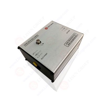
CDNE-M316_Coupling Decoupling Network
The role of the coupling and decoupling networks in surge immunity tests:
Using the coupling-decoupling network can effectively transmit the surge signal from the synthesized wave generator to the circuit of the test device, preventing the synthesized wave generator from being damaged, and reducing the influence on the surge waveform. At the same time, decoupling network can provide good decoupling impedance effect, effectively preventing the surge from entering the circuit and causing a negative effect on other devices, such as surge arresters. Therefore, by using the coupling and decoupling networks, good surge immunity can be achieved.
The structural design and circuit parameters of the coupling and decoupling networks(CDN):
There are many ways to realize the coupling network, such as capacitive coupling and gas discharge tube coupling, but since the gas discharge tube coupling significantly affects the output waveform of the synthesized wave generator, capacitive coupling is more common. In view of the relationship between output signal efficiency and residual voltage, the national standard stipulates that 18 μF capacitance is used for line-line coupling (differential mode) and 9 μF capacitance is used for line-ground coupling (common mode). When line-ground coupling, in order to ensure the virtual impedance (defined as the ratio of open circuit voltage peak-to-peak and short circuit current peak-to-peak), an additional resistance of 10Ω should be serially connected to increase the effective source impedance.
The decoupling network consists of an LC low-pass filter (decoupling inductor L and decoupling capacitor C) which can effectively stabilize the voltage at the EUT side. The equivalent circuits of line-ground and line-line decoupling networks are: Rs and R′s are the source resistances of the surge source, Rs=12Ω, s=2Ω respectively, making the voltage transmission function properly changed, so as to more effectively stabilize the voltage at the EUT side.
Read the full article
0 notes
Text
How do you protect a Thyristor from reverse voltage?
Protecting a thyristor from reverse voltage is crucial to ensure its longevity and proper functioning. Here's how you can do it:
Reverse Voltage Protection Diode: Placing a diode in parallel with the thyristor's anode and cathode terminals can help protect it from reverse voltage spikes. The diode conducts when reverse voltage is applied, providing a path for the current to bypass the thyristor.
RC Snubber Circuit: Using an RC snubber circuit across the thyristor can help dampen any high-voltage spikes that occur during reverse voltage conditions. This circuit consists of a resistor and a capacitor connected in parallel, which absorbs the excess energy and protects the thyristor.
Crowbar Circuit: A crowbar circuit is another method of protecting a thyristor from reverse voltage. It consists of a thyristor and a resistor connected in parallel with the thyristor. When reverse voltage is applied, the thyristor triggers and short circuits the power supply, protecting the main thyristor.
Fuse Protection: Using a fuse in series with the thyristor can protect it from excessive reverse voltage. The fuse will blow if the reverse voltage exceeds a certain limit, isolating the thyristor from the damaging voltage.
Proper Grounding: Ensuring that the thyristor and its surrounding circuitry are properly grounded can also help protect it from reverse voltage. Grounding provides a path for the excess current to flow, preventing damage to the thyristor.
0 notes
Text

My MP2 finally came!
Only problem is that now I have to figure out how to power it. The battery is dead and I can’t find a pinout for the proprietary MSL connector that usually powers the monitor. I can find the voltage of it but I can’t find a pinout. And let me just say that 36-56 volts is really weird especially considering that it immediately steps it down to 16 volts. So I have 2 options now, both involve opening it up and removing the main board. Then I can find the DC to DC converter on the board, and either inject 36 volts directly into its input, or bypass it completely and inject 16 volts on its output. I’ll probably do the latter since I don’t have a power supply laying around that can output 36 volts that’s not a variable AC transformer. Doing that might be a little challenging since I can’t find a schematic for it but identifying a DC to DC converter isn’t hard, since they usually have large capacitors and inductors in the circuit. If I’m lucky the DC to DC converter is on its own daughter board. I just hope the 16 volts isn’t a dual rail (positive and negative) supply because I only have a single rail power supply. Because it has digital components it also has a 5 and 12 volt power supply rail so if it just needs 5 and 12 volts and it’s making that from 16 volts and there’s no circuity to measure the 16 volts, I have power supplies that have both a 5 and 12 volt rail. Good news is I can charge the battery with my variable DC power supply. I should mention that you don’t just want to use any old DC power supply to charge a lithium battery. Lithium batteries require constant current to charge meaning you need a power supply with current regulation and limiting, otherwise the battery will draw a ton of current from the supply and probably destroy both the power supply and the battery. It’s a bit bigger than I had thought but it’s still incredibly compact for a device that has all of these measurements it can take. I already opened it up just to get a look inside, and there is no room to add anything it’s using every bit of space it has. I will say that this one is a bit harder to take apart than the MP5 because it has 2 ribbon cables for the display that are very easily broken and very difficult to put back after. It’s also very compact so getting to certain areas is much more difficult. But it’s still easier to take apart than a modern cell phone. I can fix just about anything but I have never and I never will try to fix my own phone because I know that I’ll break it.
0 notes
Text
ahh yass i just rewired my electric bass last night and it limited the heck out of what it can do but it sounds so much better now!!
my bass setup in this case is a 2004 4-string Dean Edge Hammer in ‘mahogany’ stain basswood with rosewood fretboard and the mother-of-pearl bass clef inlay. It came with some hot humbucker pickups but idk which ones or how to tell the difference or even what the options were back then. It has active electronics.


the whole time i have had it, i have been struggling to get a clean bass tone out of it and when i got a tube amp it became apparent that it is partly just way too hot of an output. of course i also found out more recently i have been using the controls completely wrong, and what i thought was a Volume, a Tone per pickup, and pickup Blend knob for a total of 4 knobs (three of which have a center detent) WAS ACTUALLY a Volume (this is the only knob i understood correctly), a Bass EQ band, Treble EQ band, and Blend was the pot i believed to be the neck pickup Tone 🤦🏻♀️🤣
So this was the RBA04 potted electronics that come in so many active basses… turns out most of the distortion i was struggling against on transients was a product of the preamp/EQ. I jumpered the blend and volume wires on the molex connector into a bypass, pulled the preamp chunk of resin, then wired the two humbucker splits to the pair of EQ pots i removed wires from. This made a Volume, Blend, and 2 Spin-A-Splits! It’s great, plays nice with fuzz other than just EHX Big Muff Pi style 4-transistor circuits now, and i somehow got by keeping the 30kilohm pots on all of it.
But i still don’t have a Tone pot… should i make one knob master Spin-A-Split and one a center detented Tone pot?? But some of single bridge and some humbucker neck sounds niiice… maybe i make the Volume a dual concentric pot with Tone and Volume?? 5 pots in 4 holes would be cool. And the 9V box can be a big ass vintage film capacitor from my 1950’s large format reel to reel line amp that was not all there and is getting turned in to other projects’ parts (it was a good outboard tone control when it was plugged)
It sounds crazy now, even though it does not make that Weather Report tone as easily.
As for the RBA04, it turns out it stands for Rock Bass Amp… lol i mostly only ever played jazz on it. The potted hunkocrap module may become my next EQ/Boost pedal if i can quiet its angry demons or use the EQ without the attacks being distorted? haha idk or just lean in to the distortion
0 notes
Text
i watched one video about bypass capacitors like over a year ago and now suddenly youtube is constantly recommending me videos about bypass capacitors. why
1 note
·
View note
Text

Specifications:-
Collector emitter voltage: -40V
Collector base voltage: -40V
Emitter base voltage: -5V
Collector current: -200mA
Collector dissipation: -625mW
Transition frequency: 250MHz
Noise Figure: – 4dB
MRPRs. 725.00
Rs. 500.00(Incl. Tax)
2N3906 General Purpose PNP Transistor
The 2N3906 PNP General Purpose Transistor is a high-performance general-purpose transistor. This transistor is a general-purpose device that provides both current amplification and voltage amplification. This transistor can also be used for high-frequency amplification. The 2N3906 PNP General Purpose Transistor is a general purpose bipolar transistor. This transistor has a hinged base which allows for easy placement of a bypass capacitor. It is a fast and efficient switching device. This PNP general-purpose transistor can be used in a wide variety of applications. It is designed for switching, amplifying, and limiting. It is most often used in electronic circuits, but it can also be used in electronic devices such as radios and TVs. The 2N3906 PNP General Purpose Transistor is a general purpose device that operates as a voltage controlled current source and is suitable for use in many different applications.
Features:-
Advanced process technology
Low error voltage
Fast switching speed
Full-voltage operation
High power and current handling capability
0 notes
Text
What is the Circuit design method in electrical engineering?

How can we design a circuit?
A circuit is any loop through which matter is carried. For an electronic circuit, the matter carried is the charge by electronics and the source of these electrons is the positive terminal of the voltage source. When this charge flows from the positive terminal, through the loop, and reaches the negative terminal, the circuit is said to be completed. However this circuit consists of several components that affect the flow of charge in many ways. Some may provide a hindrance to the flow of charge, some simple store, or dissipate the charge. Some require an external source of energy, some supply energy. This process is easy for the students of electrical & electronics engineering colleges in Jaipur.
Why We Need To Build A Circuit?
At times we may need to glow a lamp, run a motor, etc. All these devices-a lamps, a motor, LED are what we call as loads. Each load requires a certain current or voltage to start its operation. This voltage may be a constant DC voltage or an AC voltage. However, it is not possible to build a circuit just with a source and a load. We need a few more components that help in the proper flow of charge and process the charge supplied by the source such that an appropriate amount of charge flows to the load.
Most of the circuits or electronic devices require a DC voltage for their operation. Students of best engineering college in Jaipur can use simple batteries to provide the voltage, but the major problem with batteries is their limited lifetime. For this reason, the only way we have is to convert the AC voltage supply at our homes to the required DC voltage.
Process of Converting AC Voltage To DC Voltage
AC voltage from the supply at 230V is first stepped down to low voltage AC using a step-down transformer. A transformer is a device with two windings including primary and secondary, wherein the voltage applied across the primary winding, appears across the secondary winding by the virtue of inductive coupling. Since the secondary coil has a lesser number of turns, the voltage across the secondary is less than the voltage across the primary for a step-down transformer.
This low AC voltage is converted to pulsating DC voltage using a bridge rectifier. A bridge rectifier is an arrangement of 4 diodes placed in the bridged form, such that anode of one diode and cathode of another diode is connected to the positive terminal of the voltage source and in the same way the anode and cathode of another two diodes are connected to the negative terminal of the voltage source. Also, the cathodes of two diodes are connected to the positive polarity of the voltage and the anode of two diodes is connected to the negative polarity of the output voltage. For each half-cycle, the opposite pair of diodes conducts and pulsating DC voltage is obtained across the bridge rectifiers by the experts of top engineering college in Jaipur.
The pulsating DC voltage thus obtained contains ripples in the form of AC voltage. To remove these ripples a filter is needed which filters out the ripples from the DC voltage. A capacitor is placed in parallel to the output such that the capacitor (because of its impedance) allows high-frequency AC signals to pass through get bypassed to the ground and low frequency or DC signal is blocked. Thus the capacitor acts as a low pass filter.
Steps To Build the Circuit
Step1: Circuit designing
Decide the regulator to be used and its input voltage.
Have a constant voltage of 5V at 20mA with the positive polarity of the output voltage. For this reason, we need a regulator that would provide a 5V output. An ideal and efficient choice would be the regulator IC LM7805. Our next requirement is to calculate the input voltage requirement for the regulator. For a regulator, the minimum input voltage should be the output voltage added by a value of three. In that case, here to have a voltage of 5V, we need a minimum input voltage of 8V. Let us settle down for input of 12V.
Decide the transformer to be used
Now the unregulated voltage produced by the experts of BTech colleges Jaipur is a voltage of 12V. This is the RMS value of the secondary voltage required for a transformer. Since the primary voltage is 230V RMS, on calculating the turn’s ratio, we get a value of 19. Hence we have to get a transformer with 230V/12V, i.e. a 12V, 20mA transformer.
Decide the value of the filter capacitor
The value of the filter capacitor depends on the amount of current drawn by the load, the quiescent current (ideal current) of the regulator, the amount of allowable ripple in the DC output, and the period.
For the peak voltage across the transformer primary to be 17V (12*sqrt2) and the total drop across the diodes to be (2*0.7V) 1.4V, the peak voltage across the capacitor is about 15V approx. Thus substituting all the values, the value of C comes to be around 30microFarad. So, let us select a value of 20microFarad.
Decide the PIV (peak inverse voltage) of the diodes be used.
Since the peak voltage across the transformer secondary is 17V, the total PIV of the diode bridge is about (4*17) i.e. 68V. So we have to settle down for diodes with a PIV rating of 100V each. Remember PIV is the maximum voltage that can be applied to the diode in its reverse biased condition, without causing breakdown.
Step2: Circuit Drawing and Simulation
Now that students of BTech electronics engineering colleges in Jaipur have the idea of the values for each component and the whole circuit diagram, drawing the circuit using circuit building software and simulate it becomes easy.
Source: Click Here
#best btech college in jaipur#top engineering college in jaipur#best btech college in rajasthan#best private engineering college in jaipur#best engineering college in rajasthan
0 notes
Last Seen Blogs

thecoloursystem
The Colour System!!

skin-care-for-women
Skin-care-for-women

semyonchudin-blog
Семен Чудин

htworxga
Untitled
