
Don't wanna be here? Send us removal request.
Statistics
We looked inside some of the posts by mategory and here's what we found interesting.
Average Info
Notes Per Post
1
Likes Per Post
1
Reblog Per Post
0
Reply Per Post
0
Number of Posts By Type
Text
1
Last Seen Tumblr Blogs


Fun Fact
The “We are the 99%” Tumblr blog became the slogan for the Occupy Wall Street movement.
Text
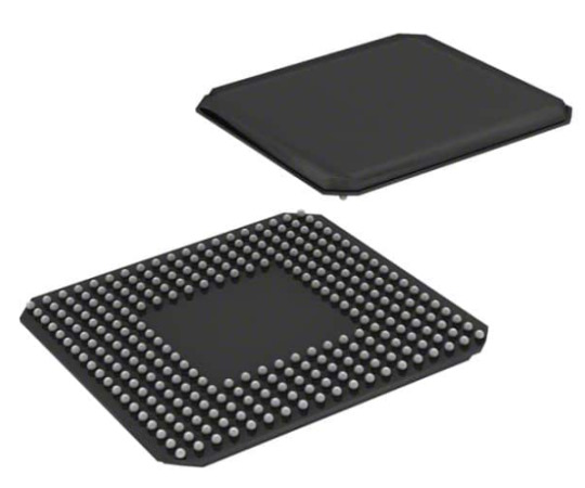
EP4CE15F23I7N
Unveiling the Power of the Intel EP4CE15F23I7N FPGA
Introduction:
The Intel EP4CE15F23I7N FPGA represents a pinnacle of programmable logic technology, offering unparalleled performance, versatility, and scalability. As a cornerstone in various electronic systems, this FPGA empowers engineers and developers to implement complex functionalities, accelerate time-to-market, and address diverse application requirements. In this comprehensive guide, we'll delve into the features, applications, and development process associated with the Intel EP4CE15F23I7N FPGA.
Understanding the Intel EP4CE15F23I7N FPGA:
At the heart of the Intel EP4CE15F23I7N lies a sophisticated architecture optimized for a myriad of tasks, ranging from embedded systems to high-performance computing.
Architecture Overview:
The Intel EP4CE15F23I7N boasts a rich assortment of resources, including programmable logic elements, embedded memory blocks, high-speed transceivers, and dedicated input/output (I/O) pins. This flexible architecture enables designers to implement complex algorithms, signal processing chains, and control systems with precision and efficiency.
Key Features:
With features such as hardened processors, configurable DSP blocks, and advanced clocking resources, the EP4CE15F23I7N offers unparalleled flexibility and performance. These features are instrumental in meeting the demanding requirements of modern applications, including machine learning, image processing, and network acceleration.
Development Process:
To fully leverage the capabilities of the Intel EP4CE15F23I7N FPGA, developers must navigate through the stages of design, implementation, and validation with diligence and proficiency.
Design Entry:
Design entry can be accomplished using hardware description languages (HDL) such as Verilog or VHDL, or through graphical schematic entry tools. Intel's Quartus Prime Design Software provides a comprehensive platform for design entry, synthesis, and verification.
Synthesis and Optimization:
During synthesis, the HDL code is translated into a hardware netlist, which is then optimized for performance, area, and power consumption. Quartus Prime's synthesis and optimization tools enable designers to achieve the desired balance between these metrics while meeting stringent timing constraints.
Place and Route:
The place and route stage involves mapping the logical design onto physical FPGA resources and determining the routing of interconnections. Quartus Prime's advanced algorithms ensure optimal placement and routing, thereby maximizing performance and minimizing timing violations.
Testing and Validation:
Thorough testing and validation are imperative to ensure the reliability and functionality of the FPGA design.
Functional Simulation:
Functional simulation allows designers to verify the behavior of the FPGA design under different operating conditions and input stimuli. Comprehensive test benches and simulation tools facilitate rigorous testing and debugging.
Hardware Validation:
Once the design is synthesized, implemented, and verified through simulation, it is deployed onto a target FPGA device for hardware validation. Real-world testing validates the performance and functionality of the FPGA design in practical scenarios.
Conclusion:
The Intel EP4CE15F23I7N FPGA stands as a testament to innovation and engineering excellence, offering unmatched performance, versatility, and scalability. By mastering its architecture and development workflow, designers can unlock its full potential and realize groundbreaking solutions across diverse industries. Whether you're designing cutting-edge data processing systems, high-speed communication interfaces, or embedded control applications, the Intel EP4CE15F23I7N FPGA serves as a reliable and powerful enabler of technological advancement.
1 note
·
View note