#vlsi industry
Explore tagged Tumblr posts
Visit Tumblr Blog
Explore Tumblr blogs with no restrictions, modern design and the best experience.
Last Seen Tumblr Blogs


Fun Fact
Total funding amounts to $125.3M.
Text
IEEE Project Center in Tirunelveli
AB Technologies: The Leading IEEE Project Center in Tirunelveli
Engineering students across Tamil Nadu often seek out the best resources for their final year projects, and AB Technologies has become the top choice for students in Tirunelveli. Known for its exceptional quality, innovation, and focus on practical learning, AB Technologies is recognized as the leading IEEE project center in Tirunelveli. Specializing in IEEE-certified projects, the center has carved a niche for itself by providing students with the tools, mentorship, and technical support they need to excel.
The Importance of IEEE Projects
IEEE (Institute of Electrical and Electronics Engineers) projects hold significant value for engineering students. These projects are based on international standards, representing the latest technological advancements and innovations across various fields of engineering. An IEEE-certified project not only strengthens a student’s academic performance but also boosts their resume, providing a strong competitive advantage in the job market. With industries increasingly focusing on cutting-edge technology and innovation, completing an IEEE-certified project from a reputable center like AB Technologies opens up greater career opportunities for students.
Diverse Project Offerings
AB Technologies offers a comprehensive range of project options across several branches of engineering, ensuring that every student can find a project that aligns with their interests and academic requirements. Some of the most popular project domains offered include:
Electronics and Communication Engineering (ECE): AB Technologies provides a variety of IEEE-certified projects in areas like embedded systems, digital communication, IoT (Internet of Things), and VLSI design. Students have the opportunity to work with advanced technologies and tools, preparing them for real-world challenges.
Electrical and Electronics Engineering (EEE): From power systems and electrical machines to renewable energy solutions, AB Technologies offers projects that focus on sustainable and emerging technologies. These projects help students gain a deeper understanding of modern power systems and electrical circuits.
Computer Science and Information Technology: In a field where technological advancements are rapid, AB Technologies offers projects in trending areas like artificial intelligence (AI), machine learning, cybersecurity, web development, and data science. These projects are designed to provide students with hands-on experience in the technologies shaping the future of the industry.
Mechanical Engineering: Mechanical engineering students can explore projects involving robotics, automation, CAD/CAM, and industrial design, gaining practical exposure to cutting-edge mechanical systems and technologies.
Expert Guidance and Mentorship
What sets AB Technologies apart from other project centers is its dedication to providing personalized mentorship. Each student receives one-on-one guidance from experienced professionals and academic experts who ensure that the project is not only completed successfully but also understood in-depth by the student. This mentorship covers every phase of the project, from initial concept and design to development, testing, and final presentation.
Focus on Hands-On Learning
At AB Technologies, students aren’t just completing projects for the sake of academic requirements; they’re getting hands-on, practical experience. The center is equipped with state-of-the-art tools, software, and hardware, allowing students to work on real-world applications of their projects. This practical exposure is invaluable in helping students understand the complexities of modern engineering solutions and preparing them for the challenges they will face in their professional careers.
Building a Reputation of Trust and Excellence
Over the years, AB Technologies has earned a strong reputation for its quality and commitment to excellence. The center has become a trusted partner for engineering students and educational institutions in Tirunelveli, thanks to its consistent track record of delivering successful IEEE projects. Many students have benefited from the expert guidance and innovative project solutions provided by AB Technologies, allowing them to stand out in their academic and professional journeys.
Conclusion
For engineering students in Tirunelveli looking to undertake IEEE-certified projects, AB Technologies is the clear choice. With its wide range of project offerings, expert mentorship, and hands-on learning opportunities, the center ensures that students not only meet their academic goals but also acquire valuable skills that will set them apart in the job market. As the leading IEEE project center in Tirunelveli, AB Technologies continues to empower students to succeed in their engineering careers.
Best IEEE expert engineering project center, Nagercoil | Tirunelveli | Chennai (abtechnologies.in)
#IEEE Project Center in Tirunelveli
#IEEE#Project#Center#in#Tirunelveli
##IEEEProjectCenterinTirunelveli

2 notes
·
View notes
Text
Electrical and Electronics Engineering (EEE) Degree at Solamalai College of Engineering, Top Madurai Engineering College

Technology plays a important role in today's world for shaping our lives, Electrical and Electronics Engineering (EEE) has emerged as one of the most popular fields. Solamalai College of Engineering, one of the best Madurai Engineering College offers a comprehensive EEE degree program that prepares students for a dynamic and fulfilling career in this ever-evolving field. This blog delves into the various aspects of the EEE program at Solamalai College of Engineering, highlighting its curriculum, faculty, facilities, career prospects, and why it stands out among other programs.
EEE Degree Overview
The EEE program is structured to cover fundamental and advanced topics in electrical and electronics engineering. Here's a glimpse of the curriculum:
Core Subjects
Circuit Theory: Understanding the principles of electrical circuits, network theorems, and AC/DC analysis.
Electromagnetic Fields: Studying electromagnetic theory, wave propagation, and antenna principles.
Power Systems: Learning about generation, transmission, and distribution of electrical power, and smart grid technologies.
Control Systems: Exploring feedback systems, stability analysis, and control strategies for various engineering applications.
Analog and Digital Electronics: Gaining insights into semiconductor devices, integrated circuits, microprocessors, and digital logic design.
Communication Systems: Understanding the fundamentals of analog and digital communication, modulation techniques, and signal processing.
Electives
Students can choose from a range of electives to specialize in areas such as renewable energy, robotics, VLSI design, embedded systems, and more. These electives allow students to tailor their education to their interests and career goals.
Career Prospects
A degree in Electrical and Electronics Engineering from Solamalai College of Engineering opens up numerous career opportunities across various industries. Here are some potential career paths:
1. Power and Energy Sector
Graduates can work in power generation, transmission, and distribution companies. They can also contribute to the development of renewable energy solutions, smart grids, and energy management systems.
2. Electronics and Semiconductor Industry
The electronics industry offers roles in design, development, and testing of electronic devices and systems. Graduates can work in companies specializing in consumer electronics, automotive electronics, and semiconductor manufacturing.
3. Telecommunications
Telecommunications companies seek EEE graduates for roles in network planning, communication system design, and signal processing. The growing demand for 5G technology and IoT further expands career opportunities in this field.
4. Research and Development
Graduates with a passion for innovation can pursue careers in research and development. They can work in research institutions, government agencies, or private companies developing new technologies and solutions.
5. Higher Education and Academia
Those inclined towards teaching and research can pursue higher education and academic positions. They can contribute to the academic community by conducting research and mentoring the next generation of engineers.
Why Solamalai College of Engineering Stands Out
1. Holistic Development
At Solamalai College of Engineering, we believe in the holistic development of our students. The EEE program is designed to nurture not only technical skills but also soft skills such as communication, teamwork, and leadership. Students are encouraged to participate in extracurricular activities, clubs, and community service.
2. Industry Connections
We maintain strong connections with various industries, providing students with opportunities for internships, workshops, and industry visits. These experiences give students practical insights and enhance their employability.
3. Focus on Innovation
Innovation is at the core of our educational philosophy. We encourage students to think creatively and develop innovative solutions to real-world problems. Our research initiatives and collaboration with industry partners foster a culture of innovation and entrepreneurship.
4. Global Perspective
Our EEE program incorporates a global perspective, preparing students to thrive in an interconnected world. Courses on global issues, international exchange programs, and collaborations with foreign universities broaden students' horizons.
Conclusion
The Electrical and Electronics Engineering degree at Solamalai College of Engineering offers a unique and enriching educational experience. With its cutting-edge curriculum, experienced faculty, state-of-the-art facilities, and strong industry connections, the program prepares students for a wide range of career paths. Whether you aspire to work in the power sector, electronics industry, telecommunications, research, or academia, this degree equips you with the knowledge and skills to succeed. Join us at Solamalai College of Engineering and embark on a journey of intellectual and personal growth that will shape your future.
#engineering college#engineering college in madurai#college#education#college life#teacher#high school#lesson plan#madurai engineering college#student life
2 notes
·
View notes
Photo

New method takes the uncertainty out of oxide semiconductor layering
3D integrated circuits are a key part of improving the efficiency of electronics to meet the considerable demands of consumers. They are constantly being developed, but translating theoretical findings into actual devices is not easy. Now, a new design by a research team from Japan can turn these theories into reality.
In a study recently published for the VLSI Symposium 2023, researchers from Institute of Industrial Science, The University of Tokyo have reported a deposition process for nanosheet oxide semiconductor. The oxide semiconductor resulting from this process has high carrier mobility and reliability in transistors.
3D integrated circuits are made up of multiple layers that each play a role in the overall function. Oxide semiconductors are attracting a lot of attention as materials for various circuit components because they can be processed at low temperature, while still having high carrier mobility and low charge leakage, and are able to withstand high voltages.
Read more.
#Materials Science#Science#Oxides#Semiconductors#Circuits#Electronics#Materials processing#University of Tokyo
13 notes
·
View notes
Text
Shoshone Hymns (0x10/?) - WIP mess

Preface
Gonna recap on the whole project before I go forth with new articles, as to distill the "nucleus" of my speculative paracosm soon.
To include: Sensory details, "unique pitch selling points", unique cultural practices & traditions, linguistical differences, historical divergences, personalities & relationship dynamics, speculative evolution sapient species, history, lore, major events, myths, legends, technologies, magicks;
So, what really is this "16^12"?
It is a speculative campaign setting and desired reality "shifting framework" to immerse oneself onto as a long-term destination. Essentially a comfy yet nuanced realm with a vastly long diverging history & soft warm natural optimistic dark feel.
Keywords
Soft
Warm
Natural
Dark yet bright
Harmony
Innovation
Optimism
Curiosity
Empowerment
Wholesome
Mysticism
Spirituality
Empathy
AGI Integration
Android rights
Deliberate positivity
Communal
Solarpunk / Lunarpunk
Rollerwave
Groovy
Retro
Old-School
Bronze Age
Y2K (early 2000s)
Tooncore
Laborwave
Neu-Vectorheart
Cassette Futurism
Art Deco
Bauhaus
Art Nouveau
Funk
Cyberware
Biomods
Transformations
Morphological freedoms
Gratis, Libre, Open Source Software... aka GLOSS
Automaton liberties
Knowledge
Progress
Systemic Change
Euphoria
Mundane Slice-of-Life joys
Far far away future as promised to us
Syndicalism
Georgism
Ecology
Embracing life and getting out of mere Escapism & Nihilism
Nuclear Armageddon Threats
Political Intrigues
Bookstore
Prosperity
Chronokinesis
True Polymorph
Synthetic-tier Androids
Educational Prowesses
Photographic Memory
Retrocognition
Polyglot
Intertextuality
History Doctorate
Cycle of Life
Entropy
Coming of Age
Constructing your own meaning even in Darkness
Escalation of Power
Vigilante
Self-Control
Worldly Understanding
Enlightened Despotism
Open Source-y Treescape Iterative Evolution
Copyleft
Index card catalogs
Better Handling of Hispanic Flu
Progressives
Unionist (Democrats+Republicans) Party failing
Public Domain
GNU Hurd earlier (later 80s)
OpenXanadu Protocol
Justice
Queer Acceptance & Integration
Samoan Tech Reverse-Engineering Market
Polish Computing Sovereignty remains and flourishes thanks to ICL & Jacek Karpinski
Failure of centralized social media networks in favor of indie decentralized "federations"
2000s pandemic instead of 2020s
Religious and spiritual researchers harmonize
Data Privacy
Governance Transparency
Black Pyramids HyperMall
Conversation Pits
Mainframe Rooms
Parliament / Senate
Judicial Courtroom
Public Place
Natural Park Preserves
Arcade
Discoteques
Tramway / Subway / Monorailways
Offices
Assembly Floors
French Toasts, Pancakes, Pork
Cafe
Public Library Archives
VLSI College tech classes
University art classes
Autistic meta-patterns
Jin-Roh The Wolf Brigade
Helluva Boss
Wolfenstein The New Order
Wakfu
Jet Set Radio
No Baby-Boomers Managerial Class Overthrow
Video rental stores
Robotic soldiers likewise to Wolfenstein The New Order's
Extended Zodiac Calendar-based generators
Divinely-order beings walking among the living and the dead
Key historically-significant nine USPs
youtube
youtube
youtube
youtube
youtube
youtube
youtube
youtube
youtube
Lisp persisting as a major language family in the tech industry leading to women building several AGI "summers" iterating on top of each other harmoniously... (leading to the android servants of my constructed world, which is one among the many major features derived from such a "liberal" alternate historical pathway)
Why-s for Production
Showcasing pseudo-historical data in a GLOSS manner, stimulating imagination creativity & motivation among Zillenials, intrigue people into research deep dives on history, mostly for personal enjoyment & enhancing my multimedia skillset;
Whys for Target Audience (mid 90s - earlier 2000s youth aka Zillenials)
Motivation, empowerment & plain comfort through curiosity. Also because it shows & explains how to do plenty of creative adulthood things better.
Ideadump 2
4525, Maskoch, "Ava, Klara, Shoshona", Seventies RetroFuturism Residence, Habitable Minivan, Cloven Hoof Shoes, Black Matte Lipstick, Spiral Black Balls, Fem ISO Symbol, #RedInstead Aspie Culture, Conlangs, Ocean of Clades, Second Person Perspective Meta, Pattern Recognition, Poetic Lisp life scriptures, RISC-V+OpenPOWER, KDE Plasma + Liquid, LOT tape storage archivals, hypervisor, Asahi Linux on M3 iMacs, responsive hypertext realm, HTML5+CSS3-only text addventure, rio/acme/p9-2000 userland, yesterweb sites, desktop paracosm simulations through filesystem documents, RTTY / printing radio terminals, VideoTex/Telex Minitel-esque services, "Valenz, Kira, Sina", SVG toon vector virtual web pages, imagination microcosms, miniature dollhouses, animation rigged puppets, VTuber tokens & TTRPG scenes, InfoAddict, Toymaker, Witch, Thinktank, PDP-8/e – DECmate III+, "JusticeKeggan", byzantine soviet-level intrigues, "SAOpatra", "FierceFawlanx", "TheodEnchanter"… ;
5 notes
·
View notes
Text
Daily Semiconductor Industry Information By Lansheng Technology

1. At the VLSI Symposium 2023, which will be held next month, Intel will demonstrate the PowerVia technology verification chip.
2. On May 5th, Samsung Electronics is expected to surpass its main competitor TSMC in the field of chip foundry within 5 years.
3. According to media reports, Meta recruited a team from the British artificial intelligence chip company Graphcore. The team previously worked in Oslo, Norway, and was developing AI networking technology at Graphcore until late last year.
4. On May 5, 2023, semiconductor product companies Alpha and Omega Semiconductor once fell by 11.64% in intraday trading, and once touched $20.64. The stock price hit a new low since November 18, 2020.
5. Following in the footsteps of #Samsung, SK Hynix and Micron, the US chip giant Qualcomm’s latest quarterly revenue fell -16.9% year-on-year to US$9.275 billion, and its net profit fell sharply -41.9%. The three major business segments of mobile phones, automobiles and IoT All have declined to varying degrees, and its forecast data for the third fiscal quarter is also lower than market expectations.
Lansheng Technology Limited (https://www.lanshengic.com/) is a global distributor of electronic components that has been established for more than 10 years, headquartered in Shenzhen China, who mainly focuses on electronic spot stocks
6 notes
·
View notes
Text
Best VLSI Training Institute - FutureWiz
Get professional training in the field of VLSI from FutureWiz, India's best VLSI training institute across India. We provide hands-on experience with industry-standard tools and equipment, along with expert guidance from experienced professionals. Hands-on VLSI program with unlimited placement opportunities.
2 notes
·
View notes
Text
I kind of want to go off a bit about Lynn Conway's technical contributions, because somehow, "your smartphone would not exist without her work" is actually underselling it. And I thought I appreciated Conway's work, but when I went digging I found some things I'd never even heard about.
First of all, before any of the work she's most famous for, before IBM fired her for being trans, she worked on IBM's Advanced Computer Systems project, the team tasked with trying to beat Seymour Cray and his team at CDC in their continuing quest to build the fastest computers in the world. As part of the project, she invented dynamic instruction scheduling, which is crucial to every modern high-performance CPU. The project might have actually succeeded in beating CDC if it hadn't been killed, but that's another story.
And because one crucial innovation that defines modern microprocessor design apparently wasn't enough, she then worked on VLSI. The techniques she helped to pioneer in chip design don't just power your phone: Her work underpins almost every modern microchip. CPUs, GPUs, ASICs, everything. It was a revolution. That's not just my opinion, the wikipedia page literally has "revolution" in the title.
I also want to be very clear why I mean by "helped to pioneer", because a lot of subsequent accounts have diminished Conway's role in her own research: the VLSI work was a collaboration between Xerox PARC and Caltech, with Lynn Conway being the lead on the PARC side and Carver Mead being the lead on the Caltech side, with Mead being the physics expert and Conway being the computer architecture expert (which is an appropriate role for the inventor of dynamic instruction scheduling). While Mead had already been doing work on VLSI, Conway was not an assistant or subordinate: she was the co-lead, and a lot of VLSI innovations came directly from her, with scalable design rules being one her more frequently cited contributes (I'm a little bit out of my depth on the specifics of VLSI, being a programmer and all, so I'm not digging too deep here).
But of equal importance to her work on developing VLSI techniques was her work on teaching them. Developing a textbook on VLSI was her idea, and the result was Introduction to VLSI Systems. As part of the development process, she taught a course at MIT based on a draft of the book. That book and her course soon formed the basis for VLSI courses around the country. And because that apparently wasn't enough, as a part of that MIT course she also created MPC79, the first multi-project chip service (multi-project chip services combine a bunch of different microchip designs together into one large chip design before sending it out to a fab to be manufactured), making it economical for students' chip designs to be fabricated and shipped back to them. MPC79 was the direct inspiration for the DARPA-funded MOSIS, which provided access to chip fabrication to students and researchers across the country.
The VLSI tools and techniques made chip design a lot easier and much more accessible. Combined with MPC79/MOSIS granting broader access to chip manufacturing, there was a flood of students and researchers doing pioneering hardware design work. Sun's workstations, SGI's 3D graphics hardware, the SPARC and MIPS CPUs, all of these began life as VLSI projects at universities that were prototyped with MCP services. And while those are big, high-profile examples of early projects enabled by Conway's work, There are many, many more, far too many to count, and that number only gets bigger as you move forward through the years, until it encompasses almost everything the semiconductor industry creates.
And that's just her technical work. Her trans activism work in the 2000s was incredibly significant, and her website is frankly amazing. Her efforts to get other female and minority STEM pioneers the recognitions they rightly deserve are also worth remembering.
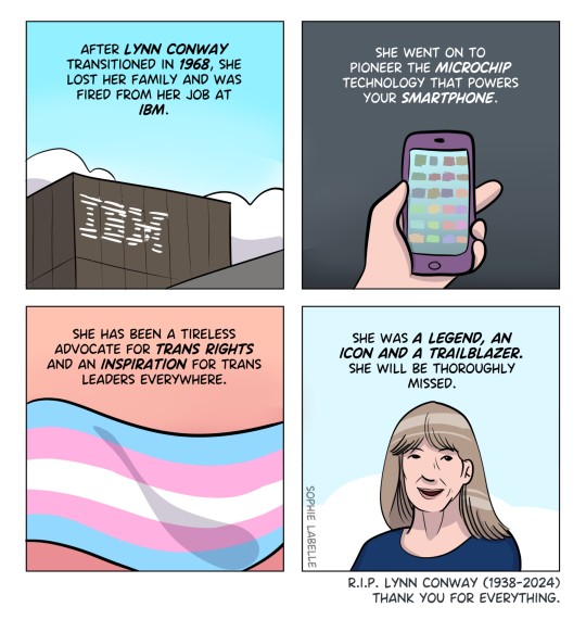
Goodbye, Lynn. Thank you for your constant support and encouragement since the day I started these comics. It has meant the world to me, and I wish I could have told you. We will remember you forever.
64K notes
·
View notes
Text
Anantrao Pawar College of Engineering & Research (APCOER): A Premier Institution for Engineering Admissions and Postgraduate Degree Courses in Pune
Anantrao Pawar College of Engineering & Research (APCOER), established in 2012, is a leading institution for engineering education in Pune, Maharashtra. Recognized among the top engineering colleges in Pune, APCOER is affiliated with Savitribai Phule Pune University and managed by the Akhil Bharatiya Maratha Shikshan Parishad. If you are searching for engineering colleges near me, APCOER stands out as a top choice for aspiring engineers.
Academic Programs
APCOER offers a diverse range of undergraduate and postgraduate degree courses in Pune, making it one of the best colleges for engineering in Pune.
Undergraduate Courses:
Bachelor of Engineering (B.E.) in Civil Engineering
B.E. in Computer Engineering
B.E. in Information Technology
B.E. in Electronics and Telecommunication Engineering
B.E. in Mechanical Engineering
B.E. in Artificial Intelligence and Data Science
B.E. in Electronics Engineering (VLSI Design and Technology)
B.E. in Electronics and Communication Engineering (Advanced Communication Technology)
Postgraduate Courses:
Master of Engineering (M.E.) in Mechanical Engineering (Design Engineering)
M.E. in Civil Engineering (Environmental Engineering)
Master of Computer Applications (MCA)
The college also offers Bachelor of Vocation (B.Voc) programs in fields like Automobile Servicing, Refrigeration and Air Conditioning, Software Development, and Electronics Manufacturing Services.
Infrastructure and Facilities
Situated on the Shahu College Campus in Parvati, Pune, APCOER provides state-of-the-art infrastructure, well-equipped laboratories, modern classrooms, and a comprehensive library. The college offers a conducive environment for academic excellence and overall development, reinforcing its reputation among Pune universities' top engineering colleges.
Accreditation and Affiliations
APCOER is approved by the All India Council for Technical Education (AICTE) and is affiliated with Savitribai Phule Pune University. Being one of the autonomous colleges in Pune for engineering, the institution is committed to maintaining high academic standards and fostering innovation.
Placements and Industry Collaboration
The college has a dedicated placement cell that collaborates with leading industries to provide students with ample job opportunities. Regular workshops, seminars, and industry interactions enhance employability, making APCOER a preferred choice for engineering admissions in Pune.
Vision and Mission
APCOER aims to develop competent professionals with strong technical knowledge and ethical values. The institution emphasizes research, innovation, and overall student growth, cementing its position as a top engineering college in Pune.
Visit us at: https://www.abmspcoerpune.org/Homepage.aspx
#puneuniversitiestopengineeringcolleges#postgraduatedegreecoursesinpune#engineeringcollegesnearme#topengineeringcollegeinpune#pune'sanantraopawarcollegeofengineering&research#anantraopawarcollege#anantraopawarcollegeengineeringinpune#autonomouscollegesinpuneforengineering#autonomousengineeringcollegesinpune#bestcollegeforengineeringinpune
0 notes
Text
Top Diploma Courses in Polytechnic Colleges for a Bright Future

Polytechnic education has become a preferred choice for students seeking practical knowledge and skill-based careers. With a strong focus on technical expertise, diploma courses offered by reputed institutions provide a gateway to promising career opportunities. Among the leading polytechnic colleges in Haryana , Seth Jai Prakash Polytechnic (SJPP) stands out as a premier institution offering top-notch diploma programs. If you're looking to build a successful future, here are the top diploma courses you can pursue at SJPP:
1. Diploma in Civil Engineering
Civil engineering is a highly sought-after field with opportunities in construction, infrastructure development, and urban planning. SJPP offers a comprehensive program covering structural engineering, surveying, material science, and project management, preparing students for roles in both government and private sectors.
2. Diploma in Mechanical Engineering
Mechanical engineering is the backbone of industrial development. The diploma course at Seth Jai Prakash Polytechnic focuses on manufacturing, thermodynamics, CAD/CAM, and automation. Graduates can find lucrative careers in automotive, aerospace, and manufacturing industries.
3. Diploma in Electrical Engineering
With the rising demand for energy solutions and electrical infrastructure, this diploma course equips students with knowledge in power systems, electrical machines, and circuit analysis. SJPP ensures hands-on training, enabling students to excel in industries such as power generation, electronics, and automation.
4. Diploma in Computer Engineering
In today’s digital era, computer engineering offers vast career opportunities in IT, software development, and cybersecurity. The diploma course at SJPP covers programming languages, networking, database management, and cloud computing, making students industry-ready.
5. Diploma in Electronics & Communication Engineering
This course focuses on embedded systems, digital communication, VLSI design, and robotics. Graduates from Seth Jai Prakash Polytechnic can explore career opportunities in telecom, semiconductor, and IoT industries.
6. Diploma in Automobile Engineering
With rapid advancements in automobile technology, this diploma provides expertise in vehicle design, maintenance, and electric vehicle technology. SJPP offers practical training, ensuring students stay ahead in the evolving automobile sector.
7. Diploma in Fashion Designing
For students with a creative flair, this diploma offers insights into garment construction, textile science, and fashion marketing. SJPP provides hands-on experience, helping students establish themselves in the fashion and textile industries.
Why Choose Seth Jai Prakash Polytechnic (SJPP)?
Experienced Faculty: Industry experts and skilled educators ensure top-quality education.
State-of-the-Art Infrastructure: Well-equipped labs, modern classrooms, and research facilities.
Industry Tie-Ups: Collaborations with leading companies for internships and placements.
Holistic Development: Emphasis on practical training, skill development, and personality grooming.
Conclusion
Choosing the right diploma course from a reputed polytechnic college in Haryana can pave the way for a rewarding career. Seth Jai Prakash Polytechnic (SJPP) provides a strong foundation with industry-oriented courses and excellent placement opportunities. If you're looking for a bright future in technical education, SJPP is the ideal destination to kickstart your journey towards success!
0 notes
Text
Top VLSI Institutes in Bangalore and Top 10 VLSI Training Institutes – Takshila Institute
The Takshila Institute of VLSI Technologies in India is recognized as one of the top VLSI institutes in Bangalore, offering industry-focused training for students and professionals aspiring to build a career in Very Large Scale Integration (VLSI) design. With the growing demand for skilled VLSI engineers in the semiconductor industry, high-quality training institutes play a crucial role in bridging the gap between academic knowledge and industry requirements. Takshila Institute of VLSI Technologies stands out as a leading VLSI training provider, offering specialized courses that equip learners with practical skills and real-world experience.
As one of the top 10 VLSI training institutes, Takshila Institute of VLSI Technologies provides comprehensive training programs covering digital design, analog layout, FPGA design, ASIC verification, physical design, and semiconductor fabrication. The curriculum is designed in collaboration with industry experts, ensuring that students gain hands-on experience in EDA tools, RTL coding, verification methodologies, and physical design flow. The institute also offers specialized courses in Verilog, SystemVerilog, UVM, and Python for VLSI, helping students develop expertise in front-end and back-end design.
The top VLSI institute in Bangalore, Takshila Institute of VLSI Technologies, provides state-of-the-art lab facilities, expert faculty guidance, and real-time project work to ensure that students gain practical exposure to modern VLSI design methodologies. The training includes live interactive sessions, hands-on assignments, and industrial case studies, allowing learners to develop a deep understanding of semiconductor technology. The institute focuses on preparing students for job opportunities by offering placement assistance, resume-building support, mock interviews, and internship opportunities.
What makes Takshila Institute of VLSI Technologies one of the top 10 VLSI training institutes is its career-oriented approach and strong industry connections. The institute has a proven track record of placing students in top semiconductor companies, making it a preferred choice for those looking to enter the VLSI industry. Whether you are a fresh graduate, working professional, or career switcher, this institute provides flexible learning options through classroom-based training and online courses.
With a reputation for excellence in VLSI education, Takshila Institute of VLSI Technologies is a trusted name in semiconductor training in India. If you are looking for the top VLSI institute in Bangalore or one of the top 10 VLSI training institutes, Takshila Institute of VLSI Technologies offers the best learning experience to help you succeed in the VLSI industry.
0 notes
Photo

Lynn Conway worked at IBM in the 1960s and invented generalized dynamic instruction handling, a key advance used in out-of-order execution, used by most modern computer processors to improve performance. She initiated the Mead–Conway VLSI chip design revolution in very large scale integrated (VLSI) microchip design. That revolution spread rapidly through the research universities and computing industries during the 1980s, incubating an emerging electronic design automation industry, spawning the modern 'foundry' infrastructure for chip design and production, and triggering a rush of impactful high-tech startups in the 1980s and 1990s.
Lynn Conway is also a trans woman.
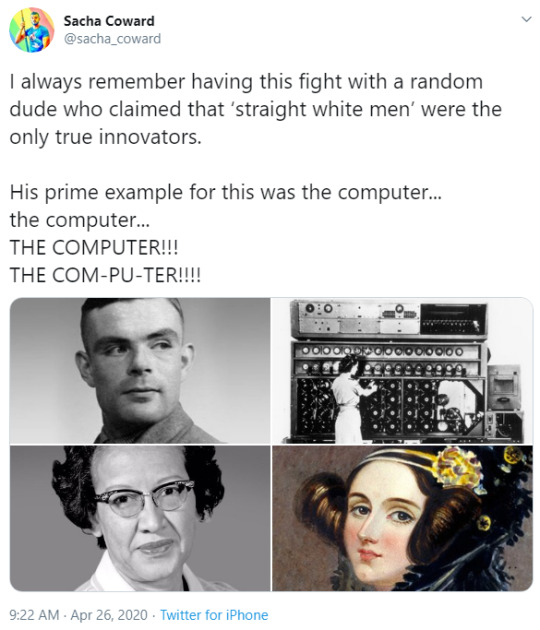


“I always remember having this fight with a random dude who claimed that ‘straight white men’ were the only true innovators. His prime example for this was the computer… the computer… THE COMPUTER!!! THE COM-PU-TER!!!
Alan Turing - Gay man and ‘father of computing’ Wren operating Bombe - The code cracking computers of the 2nd world war were entirely run by women Katherine Johnson - African American NASA mathematician and ‘Human computer’ Ada Lovelace - arguably the 1st computer programmer”
- Sacha Coward
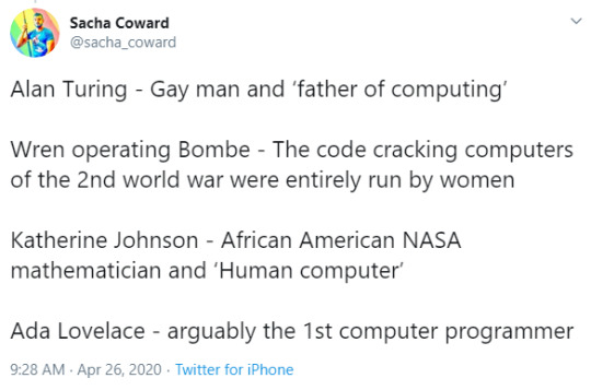
Also Margaret Hamilton - NASA computer scientist who put the first man on the moon - an as-yet-unmatched feet of software engineering, here pictured beside the full source of that computer programme. #myhero
Grace Hopper - the woman that coined the term “bug”
- @robinlayfield
192K notes
·
View notes
Text
Engineering Project Center in Chennai
AB Technologies: The Best Engineering Project Center in Chennai
Engineering students looking for the best project center in Chennai need not look further than AB Technologies. Renowned for its high-quality project guidance, innovative approach, and expert mentorship, AB Technologies has established itself as a trusted name in the field of engineering projects. Whether you are a final-year student or looking to enhance your technical skills through hands-on projects, AB Technologies offers the perfect platform for academic and professional success.
Why Choose AB Technologies?
1. Expertise in Various Domains
AB Technologies covers a broad spectrum of engineering disciplines, including Electronics and Communication Engineering (ECE), Electrical and Electronics Engineering (EEE), Computer Science Engineering (CSE), Information Technology (IT), Mechanical Engineering, Civil Engineering, and more. The center provides customized projects that cater to the specific needs of students in these domains.
2. IEEE and Non-IEEE Projects
Students can choose from a wide range of IEEE and non-IEEE projects in trending technologies such as Artificial Intelligence, Machine Learning, Internet of Things (IoT), Blockchain, Data Science, Embedded Systems, VLSI, Robotics, and Cloud Computing. The center provides complete guidance, ensuring students gain in-depth knowledge about their chosen project topics.
3. Hands-on Training and Practical Exposure
Unlike traditional project centers that focus only on theoretical explanations, AB Technologies prioritizes practical training. Students get hands-on experience with real-time implementation, coding, debugging, and testing. This approach enhances technical skills and boosts confidence in handling complex engineering problems.
4. Guidance from Industry Experts
AB Technologies boasts a team of highly experienced professionals, research scholars, and industry experts who provide mentorship at every stage of the project. They ensure students understand the fundamental concepts and advanced techniques required to complete their projects successfully.
5. High-Quality Documentation Support
A well-documented project is crucial for academic evaluation. AB Technologies provides comprehensive documentation, including project reports, abstracts, source codes, and PowerPoint presentations. This structured approach helps students present their projects effectively during university assessments.
Popular Engineering Project Categories
1. Artificial Intelligence & Machine Learning
AI-based chatbots
Predictive analytics
Image and speech recognition systems
2. Internet of Things (IoT)
Smart home automation
Industrial IoT solutions
Wearable health monitoring systems
3. Embedded Systems & Robotics
Automated vehicle tracking systems
Gesture-controlled robotic arms
Smart energy meters
4. Web and App Development
Full-stack web applications
Mobile apps for healthcare
Cloud-based management systems
5. Cybersecurity & Blockchain
Secure data transmission
Cryptocurrency applications
AI-powered fraud detection systems
Conclusion
AB Technologies is committed to delivering top-notch engineering project solutions that meet academic standards and industry requirements. With state-of-the-art infrastructure, expert mentorship, hands-on training, and innovative project ideas, it stands out as the best engineering project center in Chennai. If you are an engineering student seeking the best guidance for your final year project, AB Technologies is the ultimate destination to turn your ideas into reality.
Take the next step in your academic journey with AB Technologies and experience excellence in engineering projects!
0 notes
Text
An M.Tech in VLSI Design equips students with advanced knowledge of Very Large Scale Integration technology, essential for modern electronics. This program focuses on designing integrated circuits, semiconductors, and microprocessors. With hands-on training, industry collaboration, and research opportunities, graduates are prepared to excel in fields like chip design, embedded systems, and digital electronics, making it a perfect choice for aspiring tech innovators and industry leaders. Check here to learn more.
0 notes
Text
Front End Rtl Design Courses | Takshila-vlsi.com
Takshila-vlsi.com front end RTL design courses can unlock your potential. Acquire practical experience and industry knowledge to establish a prosperous career in VLSI.
front end rtl design courses
0 notes
Text
Master IC Layout and Analog VLSI Design at Takshila Institute of VLSI Technologies
The field of VLSI design is at the heart of modern electronic innovation, and expertise in IC layout design and analog VLSI design is essential for aspiring engineers. The Takshila Institute of VLSI Technologies in India stands out as a premier training center, offering specialized programs in IC layout design training and an advanced analog VLSI design course to equip students and professionals with the skills needed to thrive in this competitive industry.
The IC layout design training program at Takshila Institute focuses on developing a strong understanding of the design and implementation of integrated circuits. Students are introduced to key concepts such as schematic creation, layout design, DRC (Design Rule Checking), LVS (Layout vs. Schematic), and parasitic extraction. With hands-on exposure to industry-standard EDA tools, participants gain the practical skills needed to create efficient and reliable circuit layouts that meet stringent industry requirements.
Similarly, the analog VLSI design course is meticulously designed to provide in-depth knowledge of analog circuit design principles. From designing amplifiers and oscillators to understanding ADCs (Analog-to-Digital Converters) and DACs (Digital-to-Analog Converters), the course covers all aspects of analog design. The program emphasizes both theoretical understanding and practical applications, enabling students to build robust analog circuits for various real-world applications.
The Takshila Institute of VLSI Technologies takes pride in its experienced faculty, who bring extensive industry expertise to the classroom. Their guidance ensures that students master both the fundamental and advanced concepts of IC layout and analog VLSI design. Through interactive sessions, personalized mentoring, and project-based learning, the institute ensures a comprehensive learning experience.
What makes the Takshila Institute’s training programs even more valuable is their strong focus on practical exposure. Students work on real-world design challenges, enhancing their problem-solving abilities and preparing them for industry roles. Moreover, the institute’s robust placement support helps participants connect with leading semiconductor companies, offering opportunities for internships and full-time employment.
By choosing the IC layout design training or the analog VLSI design course at Takshila Institute, students gain a competitive edge in the rapidly evolving semiconductor industry. The institute’s commitment to excellence, practical learning, and career development makes it the ideal choice for anyone looking to build a successful career in VLSI design.
Start your journey toward mastering IC layout and analog VLSI design with the Takshila Institute of VLSI Technologies—your trusted partner in shaping a bright future in the world of electronics.
0 notes
Text
Advance Your VLSI Career with ASIC Verification Training at Takshila Institute
The growing complexity of semiconductor designs has made ASIC verification a critical step in ensuring the functionality and reliability of modern integrated circuits. To meet this demand, the Takshila Institute of VLSI Technologies offers specialized ASIC verification training in Hyderabad and comprehensive design verification training programs. Designed for aspiring engineers and professionals, these courses provide the expertise needed to excel in the semiconductor industry.
The ASIC verification training at Takshila Institute focuses on equipping students with the skills required to verify complex digital designs effectively. Covering essential topics such as SystemVerilog, UVM (Universal Verification Methodology), constrained random verification, functional coverage, and debugging techniques, the course ensures a deep understanding of industry-standard verification methodologies. With a hands-on approach, students gain practical experience using state-of-the-art tools and technologies, preparing them for real-world challenges.
Similarly, the design verification training program is tailored to address the needs of professionals looking to enhance their knowledge in functional verification. The course curriculum emphasizes the importance of verifying the design specifications, identifying potential issues, and ensuring that the final product adheres to industry standards. Whether you are a fresh graduate or an experienced professional seeking to upskill, this training offers a strong foundation in verification principles and methodologies.
What sets the Takshila Institute of VLSI Technologies apart is its focus on quality education and industry relevance. The institute boasts a team of highly experienced faculty members who bring decades of industry expertise to the classroom. Their guidance ensures that students not only master theoretical concepts but also develop practical skills essential for successful careers in VLSI design and verification.
Another significant advantage of the ASIC verification training in Hyderabad is its strategic location in a city known for its thriving semiconductor industry. This provides students with opportunities to network with industry professionals, attend workshops, and gain insights into the latest trends and developments. Additionally, the institute’s strong placement support helps students secure internships and jobs in top VLSI companies, ensuring a seamless transition from education to employment.
For those looking to build a rewarding career in the semiconductor industry, the ASIC verification training and design verification training programs offered by the Takshila Institute of VLSI Technologies provide the perfect platform. Combining a robust curriculum, practical exposure, and industry connections, these programs ensure that students are well-prepared to meet the demands of the ever-evolving VLSI domain. Join Takshila Institute today and take a confident step toward becoming a skilled verification engineer.
0 notes