#semiconductor assembly
Explore tagged Tumblr posts
Visit Tumblr Blog
Explore Tumblr blogs with no restrictions, modern design and the best experience.
Last Seen Tumblr Blogs


Fun Fact
Tumblr posted its first advertisements in May 2012 and subsequently earned $13M in revenue.
Text

Advances in semiconductor patterning: New block copolymer achieves 7.6 nm line width
A recently developed block copolymer could help push the limits of integration and miniaturization in semiconductor manufacturing, report scientists at Tokyo Institute of Technology (Tokyo Tech) and Tokyo Ohka Kogyo (TOK). Chemically tailored for reliable directed self-assembly, the proposed compound can arrange itself into perpendicular lamellar structures whose half-pitch width is less than 10 nanometers, outperforming conventional and widely used block copolymers. Miniaturization is one of the fundamental qualities of modern electronics and is largely responsible for the incredible increments in performance witnessed over the past decades. To keep this momentum going, it is necessary to achieve circuit patterns finer than the existing ones on semiconductor chips, which are a crucial part of all electronic devices. Some experts estimate that, by 2037, the smallest distance between features in semiconductor devices, known as "half-pitch," will need to be as small as 8 nm to support next-generation electronics, emphasizing the need for advancements in lithographic processes (method of creating highly complex circuit patterns on semiconductor parts).
Read more.
#Materials Science#Science#Polymers#Block copolymers#Semiconductors#Self assembly#Tokyo Institute of Technology
16 notes
·
View notes
Text
1 note
·
View note
Text
https://introspectivemarketresearch.com/reports/outsourced-semiconductor-assembly-and-test-services-market/
#Outsourced Semiconductor Assembly and Test Services Market Size#Outsourced Semiconductor Assembly and Test Services Market Share#Outsourced Semiconductor Assembly and Test Services Market Growth#Outsourced Semiconductor Assembly and Test Services Market Trends#Outsourced Semiconductor Assembly and Test Services Market Forecast Analysis#Outsourced Semiconductor Assembly and Test Services Market Segmentation#Outsourced Semiconductor Assembly and Test Services Market 2024#Outsourced Semiconductor Assembly and Test Services Market CAGR#Outsourced Semiconductor Assembly and Test Services Market Analyzer Industry
0 notes
Text
Outsource Semiconductor Assembly and Testing Services (OSAT Services) Market Trends, Growth, Top Companies, Revenue, and Forecast to 2032
Outsource Semiconductor Assembly and Testing Services (OSAT services) have become essential for semiconductor manufacturers aiming to streamline operations and enhance productivity. These services encompass a range of critical functions, including the assembly, packaging, and testing of semiconductor devices, allowing manufacturers to focus on core activities such as design and fabrication. By leveraging the expertise and specialized equipment of OSAT providers, companies can optimize their processes, improve product quality, and reduce time-to-market.
The OSAT sector is experiencing robust growth, driven by increasing demands for sophisticated semiconductor solutions across various industries. As technology advances, devices are becoming more complex, necessitating specialized assembly and testing capabilities. OSAT providers are continuously innovating, offering advanced packaging solutions that meet the performance and reliability requirements of next-generation applications, from consumer electronics to automotive and industrial sectors.
The Outsource Semiconductor Assembly and Testing Services (OSAT services) Market is expanding as semiconductor manufacturers increasingly outsource assembly and testing processes to enhance efficiency, reduce costs, and focus on core competencies amid rising demand for semiconductor products.
Future Scope
The future of OSAT services is promising, with substantial growth anticipated as semiconductor technology continues to evolve. As the industry shifts towards miniaturization and integration, there will be a growing need for advanced packaging solutions that can accommodate high-density designs and complex functionalities. OSAT providers are positioned to play a crucial role in meeting these needs, offering expertise in innovative packaging techniques such as system-in-package (SiP) and 3D packaging.
Moreover, the increasing emphasis on sustainability will influence OSAT services, prompting providers to adopt eco-friendly materials and processes. As manufacturers seek to reduce their environmental impact, OSAT providers will need to innovate in ways that minimize waste and promote recycling within assembly and testing operations. This shift towards sustainability will be essential for compliance with evolving regulations and for meeting consumer expectations for environmentally responsible products.
Trends
Several key trends are shaping the OSAT services market. One significant trend is the increasing adoption of automation in assembly and testing processes. OSAT providers are leveraging advanced robotics and automated systems to enhance efficiency, reduce labor costs, and improve the accuracy of operations. This trend is particularly relevant as manufacturers seek to scale production while maintaining high quality.
Another trend is the growing collaboration between semiconductor manufacturers and OSAT providers. As the semiconductor landscape becomes more competitive, partnerships are forming to leverage complementary strengths in design, assembly, and testing. This collaboration is vital for accelerating product development cycles and ensuring that new technologies are brought to market efficiently.
Application
OSAT services find applications across various sectors, including consumer electronics, automotive, telecommunications, and industrial automation. In consumer electronics, OSAT providers play a critical role in ensuring that devices such as smartphones, tablets, and wearables are assembled and tested to meet rigorous quality standards. This attention to quality is essential for delivering reliable products in a fast-paced market.
In the automotive sector, OSAT services are indispensable for the assembly and testing of semiconductor components used in advanced driver-assistance systems (ADAS), power management, and infotainment systems. The reliability of these components is paramount, as they directly impact vehicle safety and performance.
Telecommunications also relies heavily on OSAT services, with providers ensuring that semiconductor components used in network infrastructure meet stringent performance and reliability standards. As the industry transitions to 5G and beyond, OSAT providers will be instrumental in supporting the development of next-generation communication technologies.
Key Points
Essential for streamlining semiconductor manufacturing operations.
Driven by the increasing complexity of semiconductor devices across industries.
Promising future with growth opportunities in advanced packaging and sustainability.
Trends include automation and collaboration between manufacturers and OSAT providers.
Applied in consumer electronics, automotive, telecommunications, and industrial sectors.
Read More Details: https://www.snsinsider.com/reports/outsourced-semiconductor-assembly-and-test-services-market-4535
Contact Us:
Akash Anand — Head of Business Development & Strategy
Email: [email protected]
Phone: +1–415–230–0044 (US) | +91–7798602273 (IND)
0 notes
Text
The Growing Demand of Semiconductor Equipment Driving Innovation

Semiconductors: Enabling Modern Technologies Semiconductors are one of the most important components of modern electronics. They are the building blocks of technologies such as smartphones, computers, vehicles, appliances and more. As technologies become more advanced and integrated into our daily lives, the demand for semiconductors keeps rising exponentially. This growing demand is driving constant innovation in Semiconductor Device which is essential for manufacturing these tiny yet powerful components.
Semiconductor Equipment fabrication requires sophisticated manufacturing processes and precise equipment. Semiconductor Device manufacturers are continuously working to develop more advanced tools that can produce smaller, more powerful and energy-efficient semiconductors. Some of the key equipment types and technologies enabling advances in semiconductor manufacturing are discussed below.
Lithography Systems: Enabling Smaller Circuit Designs Lithography systems are used to transfer electronic circuit patterns onto silicon wafers during the semiconductor fabrication process. As circuits continue to shrink in size to accommodate more transistors in a tiny space, lithography technology needs to keep pace. The mainstream lithography technology currently used is extreme ultraviolet (EUV) lithography which uses short wavelength EUV light to print ever smaller microscopic circuits.
EUV lithography allows semiconductor manufacturers to print minimum features less than 10 nanometers across. Equipment manufacturers are ramping up EUV lithography machine manufacturing to support the transition to this advanced technology needed for the latest and future generations of semiconductors. Several companies are also developing next-generation lithography technologies like nanoimprint lithography and electron-beam lithography to take circuit scaling even further below 10nm.
Deposition Equipment: Laying Down Thin Film Layers Semiconductor manufacturing involves depositing extremely thin layers of various materials like silicon, insulators, polymers or metals onto silicon wafers through deposition processes. Chemical vapor deposition (CVD) and physical vapor deposition (PVD) are commonly used deposition techniques in the industry.
Semiconductor Equipment manufacturers are continuously optimizing deposition systems to achieve ultra-thin yet highly uniform film layers. They are building systems that offer superior step coverage to deposit films of various materials into narrow trenches and holes on complex 3D circuit designs. Advanced deposition technologies like atomic layer deposition (ALD) that allows conformal deposition one atomic layer at a time is also gaining traction for manufacturing next-generation semiconductors.
Etch Systems: Sculpting Circuit Patterns Etch systems play a vital role in semiconductor manufacturing by selectively "removing" excess deposited material to reveal the desired circuit patterns on wafers. Different etch techniques like wet etching, plasma etch and reactive ion etching are used.
As circuit features shrink to nanometer scales, etch equipment must sculpt intricate 3D structures with atomic-level precision and uniformity. Chipmakers are adopting sophisticated plasma etch systems equipped with novel process chemistries, variable frequency plasma sources and endpoint detection tools for higher resolution and selectivity. Equipment vendors are engineering etch systems optimized for materials like metals, dielectrics and compound semiconductors to enable the complex multilayered architectures of tomorrow's advanced chips.
Wafer Inspection and Metrology Tools Enabling Quality Control Error-free manufacturing of sub-10nm semiconductor structures requires comprehensive quality control. Metrology and inspection tools analyze fabricated wafers throughout the process to detect defects or quantify if critical dimensions meet tight specifications.
As circuitry becomes smaller, inspection systems equipped with powerful optics, imaging techniques and sensors down to angstrom resolutions are essential. Metrology tools employ techniques like scatterometry, medium-energy ion scattering etc to non-destructively characterize tiny structures and film layers. Automated defect inspection tools scanning whole wafer surfaces help reduce costly reworks. These enabling tools will continue scaling capabilities in lock-step with chip architectures.
Meeting the Cleanroom Challenges of Advanced Node Fabrication Another challenge is managing the contamination control, temperature, humidity and airflows needed for fabricating ever smaller circuits in tightly controlled cleanroom environments. Equipment vendors provide solutions like mini- and macro-environments, advanced filter technologies along with real-time environmental monitoring systems. This helps manufacturers achieve the stringent international cleanroom specifications required at under 10nm process nodes.
Role of Semiconductor Device in Innovation Innovations happening at the level of Semiconductor Equipment underpin ongoing progress in chip technology and the transformation of daily technology products. Continuous advancements are essential to produce smaller, more powerful semiconductors powering capabilities like artificial intelligence, augmented reality and autonomous systems. Rapidly evolving equipment solutions from lithography to metrology demonstrate the collaborative innovation between chipmakers and equipment vendors necessary to sustain Moore's Law scaling. This ensures semiconductors remain a driver for breakthrough technologies of the future. Get More Insights On, Semiconductor Equipment About Author: Money Singh is a seasoned content writer with over four years of experience in the market research sector. Her expertise spans various industries, including food and beverages, biotechnology, chemical and materials, defense and aerospace, consumer goods, etc. (https://www.linkedin.com/in/money-singh-590844163)
#Semiconductor Manufacturing#Wafer Fabrication#Cleanroom Technology#Packaging and Assembly#Lithography Equipment
0 notes
Text
#Infineon Technologies#MemorandumofUnderstanding#supplychains#Semiconductor Assembly and Test#electronicsnews#technologynews
0 notes
Text
Vibrant Gujarat: Tata Group's Bold Move with Semiconductor Plant in Dholera
In a significant stride towards technological advancement and industrial growth. Tata Group, under the leadership of Chairman N Chandrasekaran, has unveiled plans to establish. A state-of-the-art semiconductor fabrication plant in Dholera, Gujarat. This ambitious project, slated to commence operations in 2024. Was officially announced during the 10th Vibrant Gujarat Global Summit, marking. A…

View On WordPress
#tata electronics#Tata group plans for a semiconductor factory in Dholera#Tata group plans for a semiconductor factory in Gujarat#Tata group plans for a semiconductor factory in India#Tata group plans for a semiconductor in india#tata semiconductor assembly and test private limited#tata semiconductor investment#tata semiconductor manufacturing company name#tata semiconductor manufacturing company share price#tata semiconductor manufacturing plant in india#tata semiconductor plant location
0 notes
Text
OSAT companies in mainland China lower chip packaging prices
August 25, 2023 /SemiMedia/ — According to industry insiders, OSAT (Outsourced Semiconductor Assembly and Testing) companies in mainland China are lowering prices to win more orders. The utilization rate of mature wire-bonding and mid-to-high-end flip-chip packaging processes in chip packaging has not yet changed significantly, but OSAT companies in mainland China can provide more substantial…
View On WordPress
#electronic components news#Electronic components supplier#Electronic parts supplier#Semiconductor assembly and testing
0 notes
Link
#market research future#semiconductor assembly testing#semiconductor testing services#semiconductor assembly service#assembly and testing
0 notes
Text
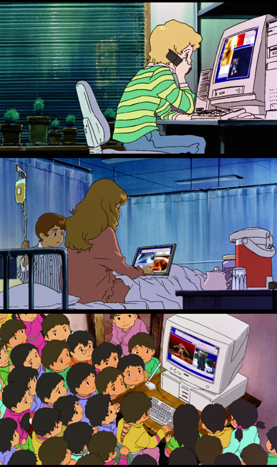
Digimon Adventure: Our War Game, Part 2 of 2
Previously on Digimon Adventure: After recovering her hat from the Digital World in a wild spinoff adventure that lasted at least 45 episodes, Mimi went on vacation to Hawaii and is living her best life. All of her friends miss her terribly to the point that Jou ended up vandalizing her family nameplate out of grief, which goes to show what a vital and important cornerstone of this team she is.
Meanwhile Tokyo's phone system is glitching out 'cause too many people are prank calling each other or something. IDK the B-plot didn't seem that important.
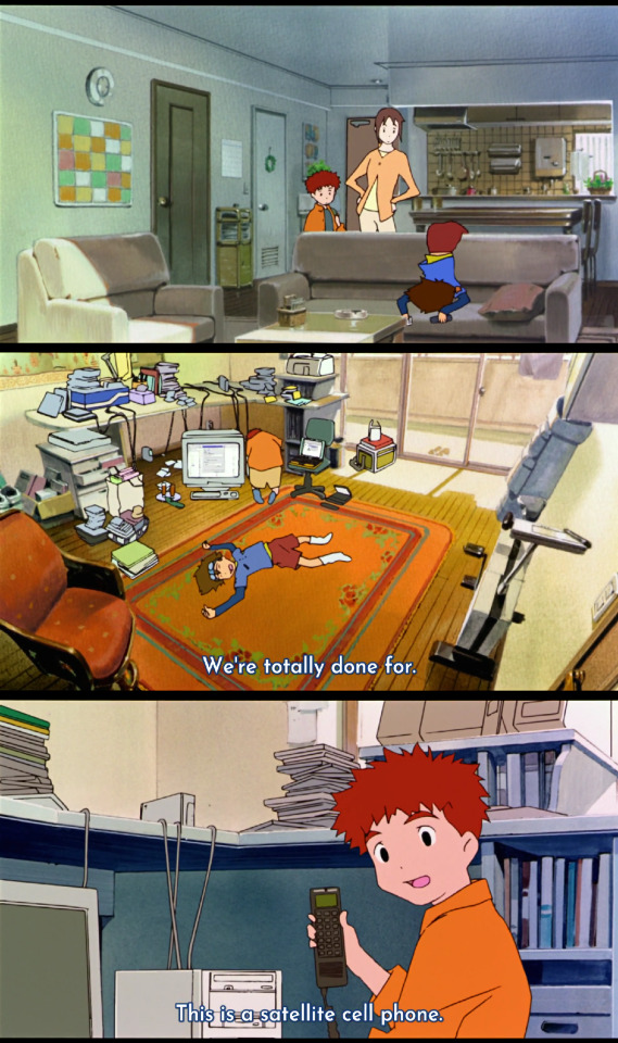
While Taichi is contemplating how unbelievably difficult the task of getting a hold of Mimi has become, Koushiro returns.
Yuuko: Oh, welcome back. Koushiro: Thank you. What's wrong, Taichi-san?
His answer is to once again flop helplessly over the couch.
Cut to the interior of Susumu's office, where Koushiro's once again at work with the computer while Taichi lies helplessly on the floor. I choose to believe Koushiro dragged him in here by his ankles.
Koushiro: Hawaii, huh? Taichi: We're completely screwed! Koushiro: We won't be able to assemble everyone, will we?
Unless we have a way of reaching Mimi in Hawaii, no. For the first time, the team's going to have to make do with whoever they have on-hand, rather than the whole crew coming together for the big fight.
Well, I say 'first time' but two out of four Dark Masters and MetalEtemon were fought that way.
Taichi: By the way, where'd you run off to?
Koushiro holds up an unusual looking black phone.
Koushiro: This is a satellite phone. Taichi: Satellite? Koushiro: With this, we'll be able to directly connect with foreign access points without having to go through NTT's switchboard. Taichi: So then we can call Yamato and the others-- Koushiro: That won't be possible. Local calls still go through the switchboard. Taichi: Oh, what the hell!
Sat phone is going to bring us back from the brink of Complete Annihilation, but isn't going to solve all of our problems.
In the dub:
Yuuko: Hi, Izzy! Welcome back! Izzy: Thank you. So, uh... When's everybody coming over? Tai: NYAAAAGH!!! (flop) (Cut to office) Izzy: Cheer up already! Tai: What happened to the good ol' days when we were a team? Izzy: We are a team, Tai. But we're just kinda spread out right now. Tai: By the way, where did you disappear to? (Izzy shows him the sat phone) Izzy: Well, I went to pick this up. Tai: What is it!? Izzy: A satellite uplink. We can get onto the internet by tapping into the military satellite system! Tai: Izzy, you're a genius! How does it work!? Izzy: Well, do you know what a semiconductor is? Tai: ...a guy who works part-time on a train? Izzy: Never mind.
The dub misses the kind of important detail that we can't call the others on the sat phone. The put the semiconductor quip where that should go.
Which is a pretty good quip. XD A funny joke that also plays off the relative difference in Tai and Izzy's knowledge bases, so there's some neat characterization embedded in it.
The dub adds that we'll be accessing "the military satellite system" specifically.
Well, if we can't use the sat phone to contact the others, there's one other option.
Koushiro: Why don't you call 171 and see if we have any messages? Taichi: Oh, right, I forgot about that!
Taichi calls the number, and he and Koushiro listen in.
Recording: Playing message. Yamato: (beep) Moshi moshi? This is Yamato. What was so urgent? Koushiro: We did it! Taichi: I knew we could count on him!
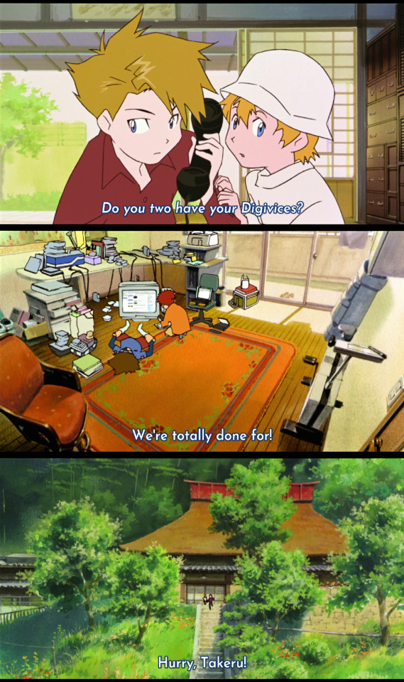
The boys record a message for Yamato, and we cut to grandma's villa.
Koushiro: (beep) You both have your Digivices, right? Yamato: Koushiro...? (Back to Yagami residence) Takeru: (beep) We have them. Yamato: Hey, what's going on here? (Back to Grandma's) Koushiro: (beep) Please find a computer to use. A new kind of Digimon appeared inside the internet. Taichi: We need you to help us fight! Takeru: ...this is really bad. (Back to Yagami residence) Takeru: (beep) We have our Digivices, but there's no computer here at Grandma's house. Yamato: There may not be any at all. We're in Shimane, after all.
The Shimane prefecture is one of the least populated regions in all of Japan. They are deeply rural right now. This realization causes Taichi to flop right back over onto the ground.
Taichi: (overdramatic) WE'RE COMPLETELY SCREEEEEEEWED!!! Koushiro: (beep) Please, try to find a computer! There has to be a computer somewhere in Shimane!
Matt and Takeru sprint out of the house, descending a long staircase from their grandmother's home.
Yamato: Hurry, Takeru!
Fingers crossed 'cause it's a ten-hour train ride back to Tokyo. We're not gonna be able to ford the Tokyo Bay on Zudomon's back with this one.
In the dub:
Tai: Is it hooked up yet? Izzy: Almost. In the meantime, check the messages to see if anyone called back. Tai: Oh! I forgot! (Tai checks messages) Matt: Hey Tai, it's Matt. So what's the big emergency? Call me back? T.K.: WAUGH!!! Matt: Oh, I gotta go. Grandma fell asleep on T.K. again. Izzy: Good ol' Matt! Tai: I knew that somebody on the team would come through! (Cut to Grandma's) Tai: (beep) Hey Matt, did you and T.K. bring your Digivices with you? Matt: Did you pack them? (Back to Kamiya residence) T.K.: (beep) This is T.K. Of course we have them! What's going on? (Back to Grandma's) Izzy: (beep) An evil Digimon has taken over the internet. Agumon and Tentomon are fighting it now but they need help! Get your Digivices to a computer as fast as you can! T.K.: ...what do we do now? Matt: (beep) Guys, the closest thing our grandmother has to a computer is an egg timer! We're going into town to find one.
The dub snips a round of phone tag, including Taichi comically flopping back over and wailing about how screwed we are. But to avoid losing the vital exposition that computers are hard to come by in Shimane, they play Matt's final message over the footage of the boys racing down the stairs.
Izzy lies to Matt and T.K. here. Agumon and Tentomon are resting, not fighting Infermon right now.
With Yamato and Takeru now on-mission, Koushiro finishes reconnecting.
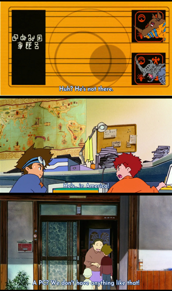
On the screen, the images of Kabuterimon and Greymon ready to fight appear. Uh, having somehow re-evolved to Adult-stage without Taichi and Koushiro connected to them. But Infermon's icon is missing.
Koushiro: Alright, we're connected! Taichi: The satellite phone worked! Koushiro: Hang on, it isn't there! Did it leave NTT? Taichi: Hey....
A new email comes in from Infermon. It has a new message, all in Katakana like the others. It reads "イナイイナイバ Inai inai ba!" Pretty sure the last letter is the creature making sounds, while いない inai in Hiragana means "Not here".
The message seems to be, "Not here not here BLEH!" Infermon is taunting them. More importantly, the email address it's using is "@@@@@@djm.dot.gov.ny.us".
Koushiro: Found it! This thing... It's in America! Taichi: America?
While that's going on, Yamato and Takeru roam the long stretches of land in Shimane searching for a functioning computer they can connect to the internet with. The first house they stop at is no good, as a man out on the porch explains to them.
Man: Computer? I have one, but it's broken right now.
At the next house, the now out-of-breath brothers are again turned aside by a middle-aged woman at the door.
Woman: A computer? I don't have anything like that.
At the third house, as the brothers now gasp for air, they're met with further failure from an elderly couple.
Old Man: A com... what? Com....
Leaving there, the boys wander the street looking for new options.
Yamato: Like I thought, there's no computers anywhere in Shimane!
Well, the good news is that when Infermon collapses society, Yamato and Takeru will be well-insulated where they are.
In the dub:
Izzy: The uplink's working! We're back online! Tai: Now let's exterminate that bug! Izzy: ...he left the phone company!? Now where is he? Tai: Look! He sent another email!
As with Infermon's previous messages, the dub rewrites the email in English. This one reads "I'm close to him." Presumably referring to Willis.
Tai: "I'm close to him"!? Close to who!? Izzy: He's in America! Tai: He doesn't even have a green card!?
By pure serendipity, this time we are in fact talking about the United States. The dub didn't have to change this one. Infermon is in America.
The following scene featuring the boys' search for a computer was cut.
Yamato and Takeru's search continues until, suddenly, they strike gold.
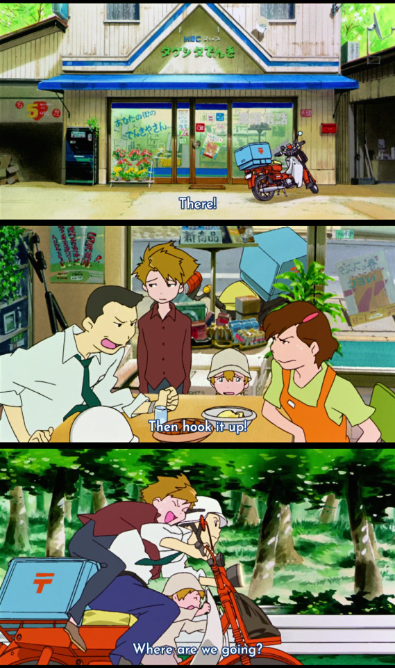
The boys discover a small storefront called タクシタでんきTakushita Denki, or Takushita Electric. Writing on the shop window generically advertises "あなたの街のでんきやさん Anata no machi no denkiya-san" or "Your town's electric appliance shop!" Probably don't need much of a pitch in Shimane.
It's not exactly Radio Shack but it's in the right ballpark so we should be able to--
Woman: I'm sorry, but I don't have an internet connection for this computer.
At this point Takeru is straight-up crying. The boys are so fucked that it provokes an argument between the man and woman running the shop.
Man: Oh come on, just let them use it. Woman: (pointed) Sho-chan, don't you have deliveries to make? Sho: I feel bad for them! Woman: (getting heated) But it doesn't connect to the internet! Man: (pounds fist on the table) Then hook it up! Woman: SHO-CHAN-- Yamato: Hey, hey, both of you....
Yamato puts a stop to this before it gets ugly, and we cut to the boys on Sho's delivery motorcycle.
Yamato: Where are we going!? Sho: Leave this to me!
Three cheers for the random deliveryman who wouldn't hang these boys out to dry.
As with the rest of the boys' search, the dub cuts the electric shop too. All we get is the boys on Sho's motorcycle, which is quickly recontextualized to explain who he is.
Matt: UNCLE AL!!! I SAID SLOW DOWN!!! Al: STILL CAN'T HEAR YOU!!!
As with "Sora's cousin Duane", the dub's invented a new relative to transport the Chosen Children. I wonder if the kids accepting rides from strangers made the censors uncomfortable?
Meanwhile, in the United States, Infermon rampages unchecked across American systems.
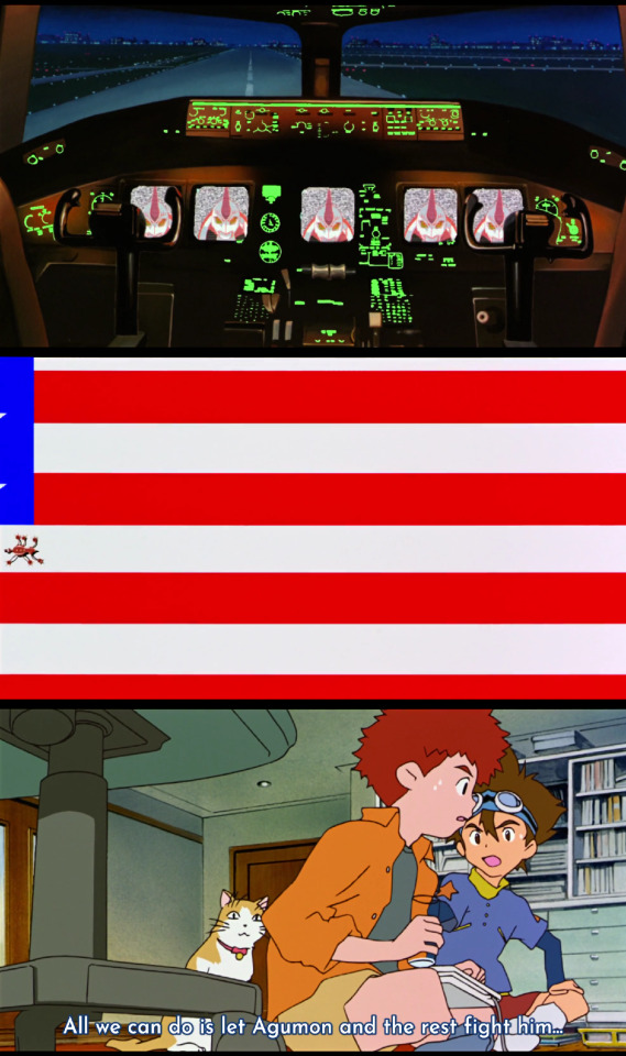
Devouring everything in its path, we see multiple effects of the havoc it's unleashing.
Bus destination signs flickering into gibberish. Cab drivers' navigation systems replaced by static images superimposed by Infermon's face. The same happening to the giant screens in New York City, as well as airplane and flight control instruments at airports.
There's also one really cool metaphorical shot, gradually zooming out on an American flag while Infermon crawls up one of its stripes like an infectious parasite. Gives me the heeby-jeebies.
Finally, we end Infermon's rampage on a shot of NYC at night, as lights flicker in every building and police sirens scream through the night.
Taichi: Bastard! It's having fun! Koushiro: Despite being Perfect-stage, it's still a newborn child. There's no way to know what it's going to do. Taichi: Can't someone do something about this? Koushiro: I'm sure there's adults out there who've figured out that they aren't dealing with an ordinary computer glitch. But they have no way of realizing that it's a Digimon causing all this. Taichi: Then... What can we do!? Koushiro: All we can do is have Agumon and the others fight it. Taichi: But even then....
Taichi is pissed. He whips out この野郎 konoyarou, one of anime's favorite vulgar Fuck Off And Die insults.
The dub plays Infermon's American rampage for fun times. They set it to the song "All My Best Friends are Metalheads" by Less Than Jake.
Izzy: Well, the Digimon's in New York. He's eaten all the data at Kennedy Airport and he's headed for the subway system. Tai: Good! That will definitely slow him down, for sure! Izzy: I'd better email Willis and let him know that Infermon is heading in his direction. I do have one question, though. What do you think that Digimon would have been like if the virus never attacked him? Tai: I have a question too: WHY ARE YOU STILL DRINKING THAT JUNK!?!? Izzy: Look, just because you don't like to eat healthy, doesn't mean that I don't. Tai: Don't say I didn't warn you....
This isn't even a different take; They flat-out replaced this scene with a brand new one. Referencing Infermon's new goal of finding Willis and making jokes (and foreshadowing) about Yuuko's recipes.
Also, Izzy ponders what Infermon would be like if it wasn't infected by the virus, which is a funny question to ask when the dub added that detail in the first place. Speaking from the Japanese side? The same, Izzy. It's the same. Without a virus, Infermon is the same.
Well. Less talkative, so the virus did change some things, but not as much as you might think.
Suddenly, the boys receive a videocall. Man, it's a good thing Infermon left NTT 'cause good luck finding a satellite phone in Shimane.
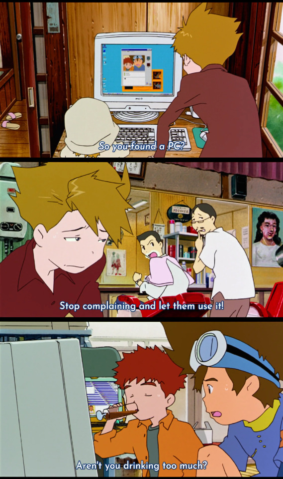
Taichi: Yamato! Yamato: Sorry to keep you waiting! Takeru: We have our Digivices! Koushiro: I see. That's good. You found a computer? Yamato: Uh, well....
Cutting to their perspective, we see that the brothers are at a computer in a barber shop. The barber does not seem very thrilled about letting them use his computer.
Barber: Are you sure it's okay to let these kids touch it? Sho: (jolts upright) Stop whining and let them use it!
While I doubt it was intentionally tactical, Takeru's waterworks worked. Sho is invested in getting the boys online. They are, however, not exactly in a private space.
Elderly Man: Those are Kinu-san's grandchildren. Elderly Woman: Life in Tokyo sure is different. Taichi: Hey! What's wrong, Yamato! Hey! Yamato: N... No... It's nothing.
Returning to Odaiba, Koushiro chugs his glass of oolong tea from the tray they brought.
Taichi: Whew. You know, I was worried there for a moment. Koushiro: Taichi-san, can I have your oolong tea? Taichi: Haven't you drank too much already?
Koushiro doesn't wait for Taichi's answer. He chugs Taichi's glass too.
In the dub:
Tai: Matt! Matt: We've got the Digivices! T.K.: Now what? Tai: Awesome! We'll tell Gennai to upload Gabumon and Patamon onto the net! Matt: You can do that? Barber: That sounds like fun! Usually I just play Solitaire on that thing, but I-- Al: (jolts upright) Careful, Floyd! You almost cut my ear off! Elderly Man: Kids today are so smart, aren't they? Elderly Woman: I still can't set the time on my VCR. Tai: Hey Matt, who are all those weird people? Matt: (loudly) They're not weird! They're my best friends! (bitterly mutters) Considering this is the only computer in town! (Meanwhile, Izzy chugs his glass) Tai: Gennai's transfer of the Digimon is almost completed. Izzy: Hey, can I have yours? Tai: (despondent) Izzy, you're the bravest kid I've ever known....
The dub adds the detail of Tai "having Gennai move Gabumon and Patamon onto the net", which is a pretty detail to add. The barber is also a lot more friendly about letting random children use his computer.
It's ironic that Random Stranger Sho is a lot more gung-ho and aggressive about helping these kids than Uncle Al. Al got them to a computer too, but he's not throwing hands with everyone in Shimane over it. XD
Inside the internet, Agumon and Tentomon fly through cyberspace, ready for another round.
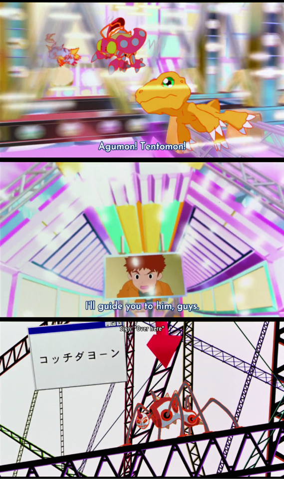
Tentomon: Aren't the others connected yet? Agumon: If not, we'll just have to fight it again by ourselves. Tentomon: Yeah, but-- Gabumon: Agumon! Tentomon! Both: Hm?
Gabumon and Patamon enter the circuit they're flying through from another tunnel.
Tentomon: Ah! Gabumon and Patamon! Patamon: We're coming too! Gabumon: Sorry we're late! Yamato: We're counting on you, Gabumon! Takeru: Ganbatte, Patamon! Koushiro: I'll guide all of you. Digimon: Okay! Agumon: This time, we'll definitely defeat this thing!
Reminder: Ganbaru is the Japanese cultural value of perseverance through tremendous adversity via hard work and dedication.
Arrows appear along the path, marking the route and guiding the Digimon to a new virtual space. This one is full of floating construction beams everywhere.
Perched atop one of those beams is Infermon, along with a video game compass marker helpfully pointing it out and a sign. A sight that has only gotten funnier in this modern age of gaming.
It's not Koushiro doing that part, though. The sign's origin is clear from the fact that it's simplistically written in strictly Katakana, like Infermon's earlier messages. It reads コッチダヨーン Kotchidayoun, which translates to こっちだよーん Kotchida youn which translates to "Over here".
Yamato: Is it playing with us!? Taichi: Yamato, let's go all out! Yamato: Straight to Ultimate level!
Yes. Yes, it is playing with us. Its age can be measured in hours. This is all a game to it.
In the dub:
Agumon: We're going back in! Tentomon: I assume Izzy and Tai were unsuccessful in finding anyone else. Agumon: Then you and I will just have to beat that thing by ourselves! Gabumon: Sorry we're late! Patamon: I was surfing the net and I wiped out! Agumon & Tentomon: Huh!? Tentomon: Gabumon and Patamon! Patamon: Is T.K. on this ride? Gabumon: He's not tall enough. Yamato: Hey, Gabumon! T.K.: Patamon! Izzy: Say hello later! We have work to do! Tentomon: Keep your legs and wings inside this ride at all times! Izzy: Just a little further, guys. Just remember: He's dangerous so stay focused! (The Digimon spill into the new area of the internet) Infermon: I'm looking for the programmer; Don't interfere! Matt: He's teasing us! Tai: Oh, yeah!? Then let's get him! Matt: It's time to Digivolve!
Patamon "surfing the net and wiping out" is a nice bit of wordplay for his punny quip, though I'm not sure what it's supposed to mean in a literal sense.
Izzy does not offer to guide the Digimon to their destination, the message remains untranslated in Katakana, and Infermon explicitly wants them to stay away from him rather than goading them. So. I sincerely have no idea who put the pointing arrow over Infermon in this version. It just kinda happens.
As Taichi and Yamato agreed, it's time to evolve straight to Ultimate.
While Agumon and Gabumon Warp-Evolve, we jump around the globe once again to people watching their evolution sequences. This fight, too, will be broadcast worldwide.
I'm really fond of how this is presented. Show Me Your Brave Heart begins like usual when the Digimon evolve, but we jump to a different country and different group of people with each note of the song.
The dub uses their typical Warp Digivolve reprise of their opening theme, but they aren't able to time the shots to the notes for obvious reasons. It still flows pretty well.
Also, for Digimon: The Movie synergy, there's a blond boy watching in one of the shots that you could totally assume is Willis. Maybe he is! Or he could be Michael from 02. Who knows.
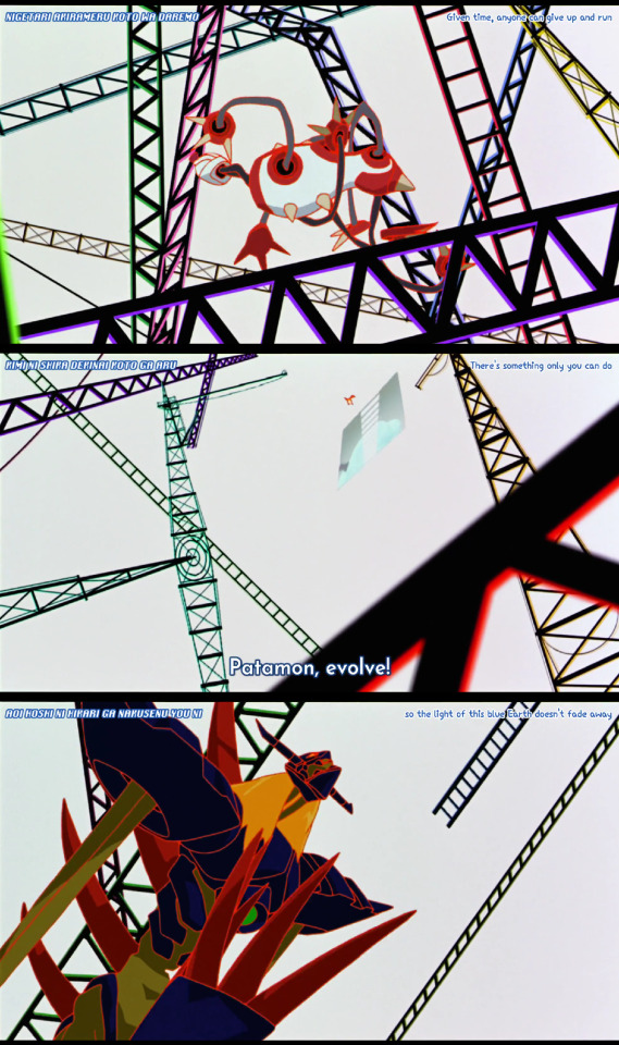
WarGreymon and MetalGarurumon take turns boxing Infermon around, making hit and run swipes at it.
Taichi: Nice! Takeru: Patamon, you evolve too. Patamon: Uh-huh!
A neat detail of Patamon's attempted evolution is that the stock animation footage appears diegetically on a screen directly behind him. We see him with the screen at an angle while the startup "Digivice meter rises and overtakes the Digivice" bit plays.
(This might be why Infermon can interfere with evolution sequences. Others have fucked with evolution before but not this directly. It's never been implied that a Partner Digimon in-universe stands there frozen in place for upwards of 40 seconds when evolving.
But we're not in the Digital World right now. We're inside the internet itself, so maybe the data stream is something that can be seen and interacted with. Or something.)
Whatever the case, Infermon's not letting them get away with this one. It lunges, undergoing its own evolution into Diablomon.
Yamato: It evolved!? Taichi: How is it so fast!?
I'm not sure if Taichi means it's moving fast, it evolved fast without a fancy sequence like the Partners have, or that it evolved quickly in the sense that it's gone from Digitama to Ultimate in the span of like a few hours. Honestly, all of these are valid questions.
In its new form, Diablomon has stretchy rubber-band limbs, which it demonstrates by punching Patamon out of his evolution sequence and pinning him against a girder.
Takeru: Patamon! Tentomon: Patamon--DAUGH!!!
Also, it has two arms, so Tentomon can have one too.
In the dub:
T.K.: Patamon, you'd better Digivolve! Patamon: Right! Patamon, Digivolve To.... Infermon: Infermon, Digivolve to: Diaboromon!
"Diaboro" is an obvious r/l mistranslation of "Diablo", the Spanish word for devil. What's less obvious is whether they did that by accident or on purpose. Might be an error, might be they fudged the name on purpose to remove the Satanic reference. Both are plausible.
Matt: What's going on!? Tai: He Digivolved.... Diaboromon: CABLE CRUSHER!!! (Diaboromon punches Patamon out of his evolution) T.K.: Look out, Patamon! Tentomon: I'll save him! (gets punched)
The stretchy arm punches are called Cable Crusher in the dub.
Gotta love T.K. yelling "Look out!" like a second after Patamon already got hit. XD THANKS. HELPFUL.
Takeru and Koushiro check on their pinned down Partners.
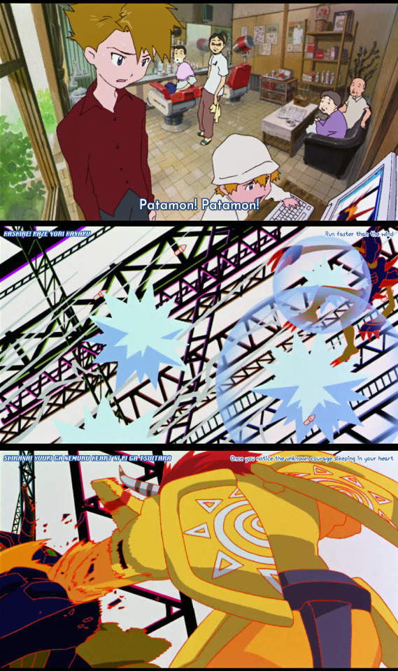
Takeru: PATAMON!!! ARE YOU OKAY!?!? Koushiro: Tentomon! Tentomon: I'm fine... Patamon.... Takeru: (crying) Patamon, I'm coming to you! Patamon! Patamon! Patamon!
Meanwhile, at the barber shop, everyone's dropped what they're doing to stare at these strange boys getting very emotional about whatever they're doing on the internet. Even Sho and the barber have stopped midway through Sho's shave.
Yamato: How dare you... HOW DARE YOU DO THAT TO PATAMON!!! Taichi: YOU'LL PAY FOR THIS!!!
Resuming the fight, MetalGarurumon goes for Diablomon first. MetalGarurumon unloads his freezing missiles, Diablomon gets pummeled by MetalGarurumon's shots. At speed, it's hard to tell if the blasts are hitting it or if it's dodging, but the freeze-frame clearly shows Diablomon getting tossed around.
Recovering, Diablomon returns fire with a fireball from its chest which hits MetalGarurumon dead on.
WarGreymon pushes through the smoke and closes distance. Diablomon tries to deflect WarGreymon's attack at range, using its own stretchy claw to break WarGreymon's right Dramon Killer off. WarGreymon adapts, turning a stab into a punch and breaking Diablomon's goddamn face.
Taichi: Tentomon! Look after Patamon. WarGreymon, stay on the attack!
Koushiro, next to Taichi, begins sweating and seems to be having, let's say, trouble with something....
As WarGreymon closes distance, the process repeats. Diablomon snaps off WarGreymon's other Dramon Killer, and WarGreymon connects an unguarded left hook into Diablomon's face.
In the dub:
T.K.: Ahh! Patamon, are you alright!? Izzy: Tentomon! Tentomon: I'm fine! What about Patamon? T.K.: Patamon! Speak to me! Come on, get up! Say something! I'm coming! I'll come get you! Matt: T.K.... You can't. (to MetalGarurumon) BUT YOU CAN!!! Tai: WIPE HIM OUT!!!
The dub names MetalGarurumon's missiles Ice Wolf Spikes, despite usually calling it (and most of his other moves) Ice Wolf Claw. Diablomon's fireball is Web Wrecker. WarGreymon's punch is just a punch, though to be honest I was expecting it to be Terra Force or, like, Nova Punch or something. XD
Tai: Tentomon, circle around! WarGreymon, attack!
For some reason, the dub has Tai tell Tentomon to "circle around" Diablomon, as if he's supposed to be moving in for a flanking strike. Um. No. His job is to go make sure Patamon didn't die a moment ago.
Unfortunately, while this is happening, Koushiro continues to have his crisis.
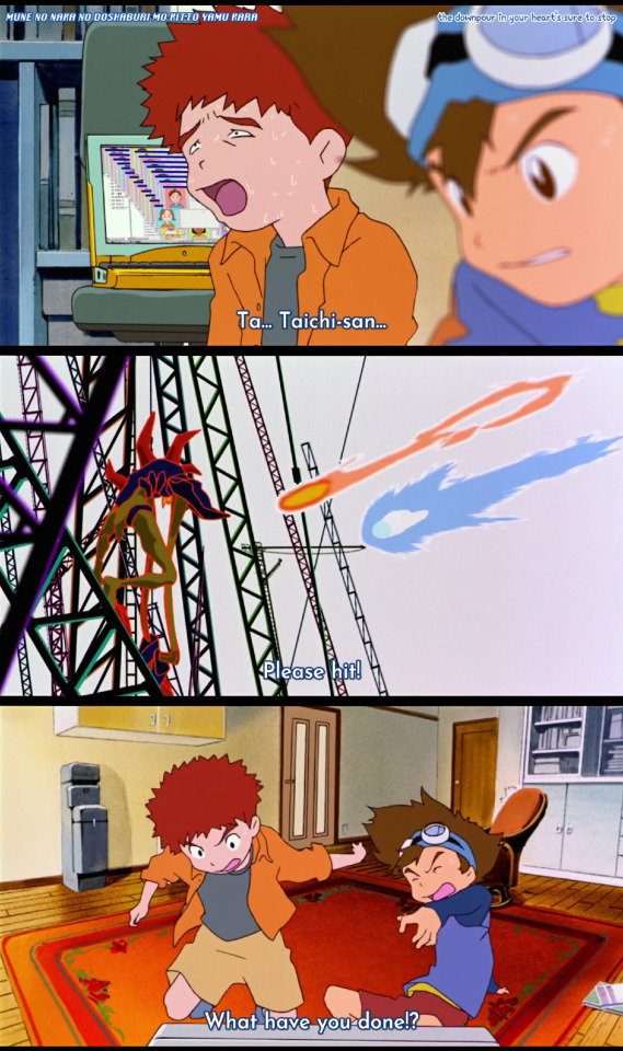
Koushiro: T-Taichi-san.... Taichi: Go! Keep it up! Koushiro: (straining) Taichi-san! Taichi: Right there! Get it! Koushiro: TAICHI-SAN!!! Taichi: The hell!?
Startled, Taichi finally turns his attention to Koushiro, who is visibly in a lot of pain.
As Taichi turns his attention to Koushiro, the line "Show me your brave heart" from their triumphant battle theme gets stuck. The soundtrack begins stuttering, playing that same line over and over and over like a broken record. Our first warning that things are now suddenly going awry.
Koushiro: I can't hold it anymore.... Taichi: What!? Koushiro: I have to use the bathroom, please....
Without another word, Koushiro stands up and staggers out of the office.
Taichi: (dismayed) Hey... Why now of all times...? Hey!
Meanwhile, in the fight, WarGreymon and MetalGarurumon both power up their attacks to throw at Diablomon.
Yamato: That's it! Finish it off! Taichi: Huh!?
The pair fire off attacks together that... Sort of look like Cocytus Breath and Gaia Force reimagined by a new art direction.
Taichi: Please! This has to hit!
It does not. Diablomon leaps straight up and hurdles their shots at the last second.
Taichi: FUCK!!!
Frustrated, Taichi smacks the computer monitor and causes it to Blue Screen. He freezes in horror when he realizes what he's done.
Yamato: What's happening, Taichi!? WarGreymon stopped moving!
This is karma for the Andromon episode of the Devimon arc, where Taichi kept smacking computers.
Taichi tries shaking the monitor a couple of times to try and get the connection back, but it's hopeless. Thankfully, Koushiro returns from the bathroom here to discover what Taichi's done.
Koushiro: Sorry about that. Taichi: (desperate, teary) It isn't working! Koushiro: Eh!? WHAT HAVE YOU DONE!?!?
Our polite little Koushiro shoves Taichi away from the computer so that he can get this fixed.
Taichi: I didn't do anything! It's your fault for using the bathroom at a time like this! Koushiro: It's useless.
Koushiro gives up on trying to get the system back on and hard reboots the computer instead.
In the dub:
Izzy: It's... no... use.... Tai: What are you talking about!? We're winning! Izzy: Owaaaaaaugh... goh... This could be it.... Tai: Yeah! Great, huh? Izzy: Not that! Tai: What's going on!? Izzy: There's something... wrong with me.... Tai: What is it!? Izzy: I think it's your mother's recipes.... (Izzy runs off for the bathroom) Tai: See!? I hate to tell you I told you so but... I told you so!
In the original, he just needs to pee. He drank too much oolong tea and now his body needs to drain the excess fluid. He leaves Taichi unsupervised with the computer for less than a minute.
Here, he's got some kind of indigestion or food poisoning going on, which will be similarly quick to handle.
Matt: Tai! Look! Something's wrong! Tai: Huh!? (The Digimon attack) Tai: Oh no! They're slowing down! (Diaboromon dodges) Tai: Huh!? COME ON!!! (Tai smacks the computer and it blue screens) Matt: Tai, where'd you go!? WarGreymon has practically stopped moving! (Tai shakes the computer a couple of times) Tai: Oh no! Oh no! Izzy: (returns) Ah, I feel a lot better. Tai: I didn't touch anything, I swear! Izzy: AH!!! (shove) TAI, WHAT DID YOU DO!?!? Tai: It wasn't my fault! Besides, who told you to go to the bathroom at such an important time!? Izzy: Like I had a choice!
In the original, Taichi and Yamato are gung-ho about landing these shots and finishing off Diablomon. The dub asserts that they're moving slower, which is a later plot point that the dub's incorporating early.
They may have brought this in early to explain why WarGreymon suddenly shuts down when Tai's connection breaks. It's never been a thing before that a Digimon suddenly goes into stasis if their Partner isn't nearby. That's a weird thing for the original to have happen, so the implied whatever-the-fuck could be an attempted story patch.
While the computer's rebooting, Koushiro vents at Taichi.
Koushiro: Why did you freeze the system!? Taichi: I didn't think that would happen! Koushiro: This is why you're bickering with Sora! Taichi: (wounded) I did nothing...!
Jesus. I don't think we've ever seen Koushiro this upset, and he once fought a guy that wanted to eat his parents. Taichi is silent for a moment, nursing the critical hit that remark struck.
Taichi: I just... (mutters) ...got her a present. Koushiro: A present?
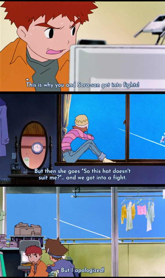
We cut to Sora, sitting in her windowsill and watching a jet go by in the sky as Taichi finally opens up about what happened.
Taichi: Her birthday was coming up, so I got her a hairclip. But then she starts saying things like, "(sneering) Oh, you think this hat doesn't suit me!?" So we started fighting....
As Taichi finishes his story, we return to Taichi and Koushiro, with that same jet visible out the window. They're far apart, physically and emotionally, yet under the same sky all the same.
Koushiro: So that's it... Taichi: Yeah, but... I'm supposed to apologize, right?
Taichi's impression of Sora, literally the tone he uses when quoting her, is mean and uncharitable. But that's not unexpected for someone who's in the midst of a quarrel and doesn't understand what he could possibly have done wrong. So far as Taichi figures it, Sora snapped all of a sudden over the hairclip and started yelling at him for no reason.
Okay. We need to take a moment and talk about the hairclip. What did Taichi do wrong? Well. They don't give us a lot of information to go on. We never hear Sora's side of the story. This is all we get.
But from what we know of Sora, we can surmise some things. The explicit point of contention is Sora's hat. Taichi gave her a pretty hairclip and her kneejerk reaction was that he was telling her not to wear her hat.
This is what she's reacting so negatively to; The implicit statement Taichi hadn't realized he was making that Sora's hat is bad. Or, specifically, that it is 似合わない niawanai, unsuitable for her. That she is the kind of person who wears pretty hairclips and not the kind of person who wears hats like this.
Let's take a moment to think about the context Sora exists in. The longstanding personal drama of her life is her conflict with her mother's expectations. Her mother is iemoto, the grandmaster for a school of ikebana, a traditional art of flower arranging. Sora was born to step into the shoes of a very traditional and feminine discipline, which she did not take well to.
Rather than following eagerly in her mother's footsteps, Sora became more invested in sports, a traditionally masculine activity. She presents herself with long pants, short hair, and that big helmet over most of her head, which she's now swapped for a floofy winter cap. She has conversations with Mimi about how assertive and strong she is compared to the more feminine Mimi.
Sora has, for years, felt like her self-expression is under siege by expectations of traditional femininity. And then Taichi comes to her and implicitly says to her, "Hey, you should change your self-expression to be more feminine." Of course she blew up. Of course she did.
Taichi, of course, had no idea the hairclip would be taken that way. He's... just... terrible at understanding other people's feelings. This was stupidity, not malice. But even though Sora and Toshiko have reconciled, that doesn't mean all the sore spots have disappeared. Taichi stepped on an emotional landmine buried in the Demilitarized Zone that Sora and Toshiko's arguments left behind.
Not to be too charitable to Taichi since he was there when she explained all this. He's an idiot who doesn't think things through and isn't good at understanding people. But he didn't mean any harm by it and now has no idea why it created so much tension.
In the dub:
Izzy: Oh, why did you crash the computer!? Now I have to reboot! Tai: Well, it's not like I did it on purpose or anything! Izzy: Yeah, right! Just like it wasn't your fault with Sora! Tai: That wasn't... my fault... Oh, okay, maybe it was my fault. Izzy: What happened? (Cut to Sora) Tai (V.O.): It was stupid. I gave her this really great hairpin for her birthday and then she got all mad and said, "(sneer) Oh, you don't like my hairstyle!?" and I said "Who could tell? You're always wearing a hat!" and then she said "So! Now you don't like my hat, huh!?" It's very confusing. (Cut back to Tai and Izzy) Izzy: That's what you fought about? Tai: I tried to apologize to her but she won't return my phone calls!
Tai and Sora's argument in the dub is a bit longer. A subtle but critical difference here is that Sora in the original is getting mad over whether her hat is suitable to her while Sora in the dub is getting mad over whether Tai personally likes her aesthetic.
Suddenly, the computer finishes reconnecting with an audible chime.
Koushiro: Ah! We're back to normal. Taichi: WarGreymon-- Ah!
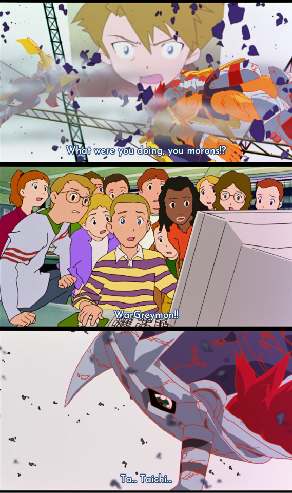
The boys reconnect to find the battlefield they left behind has become a debris field. WarGreymon and MetalGarurumon lay motionless, lifeless amid the debris.
Yamato: TAICHI!!! KOUSHIRO!!! WHAT THE HELL WERE YOU GUYS DOING!?!? YOU GODDAMN MORONS!!!
Koushiro's only crime was having to pee, and his Digimon was barely even a participant anyway. He probably doesn't deserve to be called 馬鹿野郎 bakayarou, which is the anime classic 馬鹿 baka or "stupid" but in a really mean and vulgar way. It's for when you wanna call someone baka but spit it like a curse word, no playing.
For Taichi, however, the obscenity is well-warranted.
Taichi: (teary-eyed) WarGreymon! WarGreymon! WARGREYMON!!! WARGREYMOOOOOOOOOOOON!!!
While Taichi's screaming for his Partner, we take another cuts around the globe. To all the people silently watching in stunned horror as he all but begs his Partner to be alive.
WarGreymon: T... Taichi....
Finally, Taichi's voice reaches WarGreymon and he opens his eyes again.
The dub catches that an audio cue is supposed to alert the boys, and uses that old 90's dial-up tone.
Izzy: Ah! We're back online! Tai: WarGreymon! (Debris field, half-dead Digimon) Matt: Hey guys, where were you!? You two sure picked a lousy time to take a lunch break! Tai: (teary-eyed) What happened to him!? WarGreymon! (Silence as we jump around the globe, then back to WarGreymon) Tai: WarGreymon.... WarGreymon: ...ugggggh... Tai, I can't move!
The emotions are dialed back quite a bit here. Matt gives them a snarky scolding instead of yelling obscenities in Tai's face while Tai's fear and grief doesn't quite match the bloodcurdling screaming that Taichi's doing.
Good news is that WarGreymon isn't dead. But this is still pretty bad.
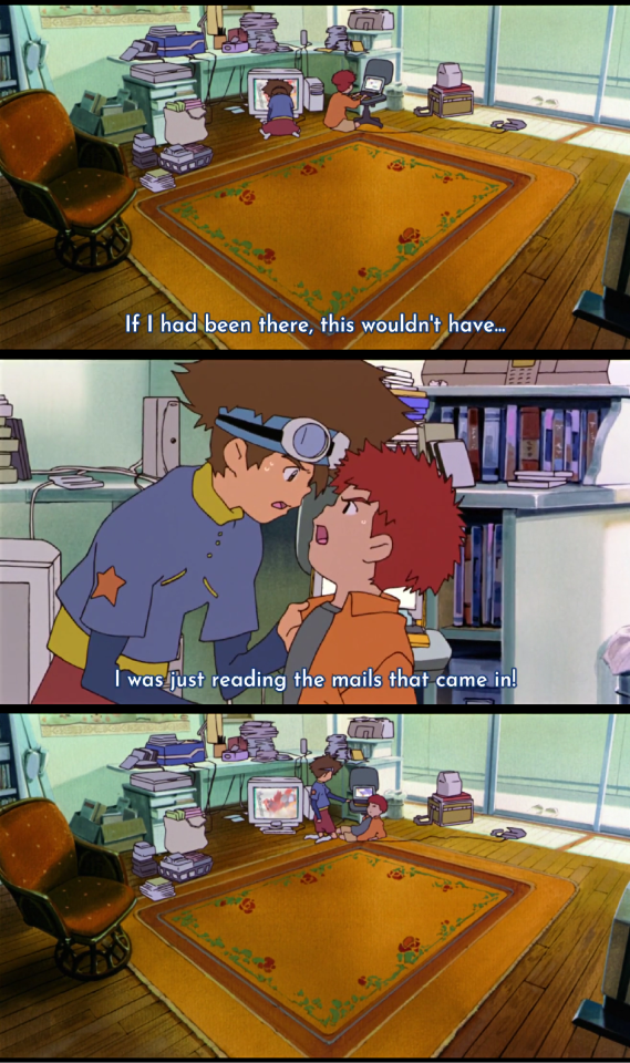
Taichi: If I.... If I'd been here, this wouldn't have happened. Koushiro: You lost again? Taichi: WHAT!?!?
Taichi whips around like them's fightin' words to see Koushiro reading emails from the laptop.
Koushiro: And now from Canberra: "You were so close to winning. What were you doing!?" This one's from Berlin--
Out of nowhere, Taichi shoves Koushiro. Then he grabs him by the scruff of his shirt.
Taichi: The hell!? ASSHOLE!!! Koushiro: I was just reading the emails we received! Taichi: Koushiro, you piece of-- Yamato: Cut it out! This isn't the time to fight each other! (beat) Taichi: Keh!
Taichi pushes Koushiro back to the ground and returns his attention to the computer.
Taichi: What's with these emails anyway!?
What gets me about this bit is that it's not a misunderstanding. His この野郎 konoyarou comes before he clarifies, but even after, Taichi still gives him a 手前 temae. That's the second-person pronoun you use when you want to say "you" in a way that expresses contempt.
Taichi isn't confused here; He is legit trying to punch the messenger.
In the dub:
Tai: I let him down! I should have been there! Izzy: Your Digimon's a loser. Tai: What did you say!? Izzy: How could two Mega-level Digimon get beat by one lousy bug!? WarGreymon quit like a coward--OW!!! (Tai shoves Izzy and grabs him) Tai: YOU TAKE THAT BACK OR I'LL-- Izzy: I WAS READING AN EMAIL FROM ANOTHER KID!!! Tai: You didn't have to read it so well! Matt: Hey, you two! This isn't the time to be fighting! (beat) (Tai shoves Izzy down and goes back to the computer) Tai: Stupid emails....
The dub does play this more for misunderstanding. They take out the parts where Koushiro says "This one's from Canberra" and "This one's from Berlin", so it sounds to Tai like Izzy's being mean and cruel out of nowhere.
Tai doesn't apologize after Izzy clarifies, but he also doesn't double down like Taichi does.
Additionally, the kids emailing seem to be a lot better informed than in the original. It's not too big a deal that they can namedrop WarGreymon since Tai/chi says his name multiple times while begging him to be alive. But they also name-drop Mega Digimon and seem to understand what that means.
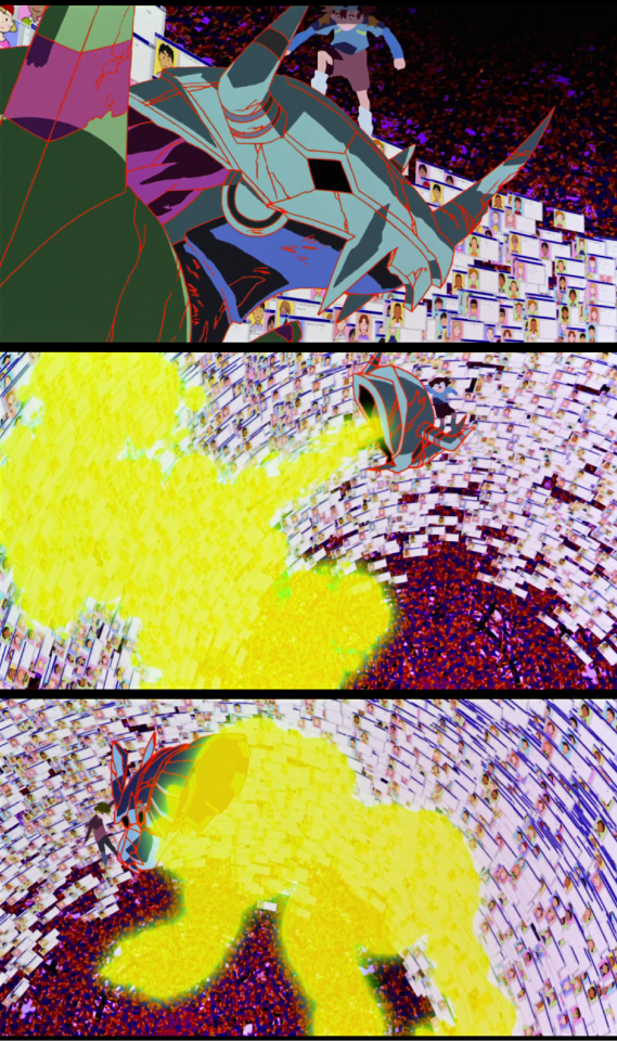
From here, we go to Diablomon in the depths of the internet.
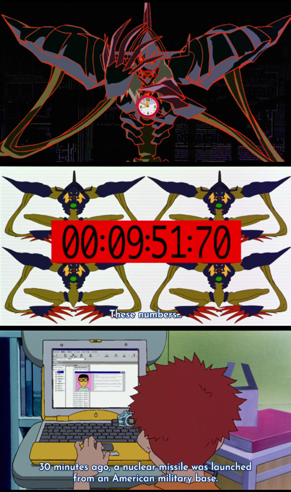
It's holding a cute pink clock, revealed to be the true source of its weird cackling back in the first Infermon fight.
Clock: Yahahahahahaha! Yahahahahahaha! Yahahahahahaha!
Diablomon waves its hand over the cackling clock and makes it disappear. Cut to an ominous shot of the jet flying in the sky, and then back to the boys.
Diablomon appears on the computer screens in front of Yamato, Takeru, and Taichi. It doesn't send an email this time; It simply composes one in real-time for them to see, typing out letter by letter.
Diablomon types トケイヲモッテイルノハ ダーレダ Tokei wo motteiru noha daareda. Which translates to 時計を持っているのは誰だ Tokei wo motteiru noha daareda. Which translates to "Who has the clock?"
Incidentally, this message is sent from the FactoryMark server so it looks like Diablomon's back in Japan. It did what it needed to do in the U.S.
Takeru: Clock?
This message is then replaced by two entirely different things to freak out about. The first is a red timer counting down from ten minutes. The second is Diablomon's image in the background dividing into two, and then those two dividing into four. Then those four into eight.
Yamato: It's copying itself.... Taichi: These numbers-- Koushiro: What do we do!? Taichi: Huh!?
Koushiro isn't looking at the screen. He's still at his laptop reading emails.
Koushiro: A middle school student from Taiwan hacked into the Pentagon, and they say that a nuclear missile was launched from an American military base thirty minutes ago. Taichi: HUH!?!? Koushiro: It was fired by a computer error. (freaking out) Of course, it was actually that thing that did it! Taichi: Then this number is.... Koushiro: The estimated time until the missile reaches its target.
OH. OKAY.
THAT IS PROBABLY BAD.
In the dub, Diaboromon talks over the ticking of the clock, which is not itself cackling.
Diaboromon: Wahahahahahaha! Go back to the beginning....
His email is rewritten in English once again. This time he types out, letter by letter, "Who can count backwards from ten?"
Tai: Another email!? "Who can count backwards from ten?" Huh!? Is he giving us a math test!? (Cut to T.K. and Yamato) T.K.: What's that? (Timer appears and Diaboromon begins dividing) Matt: Hey, what's with the timer? Tai: He's making copies of himself! (Cut back to Tai and Izzy) Tai: He's multiplying! Izzy: It gets worse! The U.S.A. just launched two nuclear missiles! Tai: Huh!?
Yep, there's two missiles in this version. Also, they were recently fired, as opposed to having been fired half an hour ago.
The dub edits the footage again to remove Koushiro's Taiwanese pal and replace him with Willis.
Izzy: Willis says the government has no explanation for it, but he found out that Diaboromon's in the Pentagon's computers. I hope I didn't lead him there with my satellite uplink! (gasp) One of the missiles is headed for Colorado! THEY'RE GONNA LAND IN LESS THAN TEN MINUTES!!! Tai: That explains the timer. But what's in Colorado!? Izzy: I have no idea! In the meantime, Diaboromon keeps multiplying!
Willis, of course. One missile for the original target and a second missile for Willis.
We cut again briefly to the "jet" leaving its trail in the air. Now with an unsettling new context.
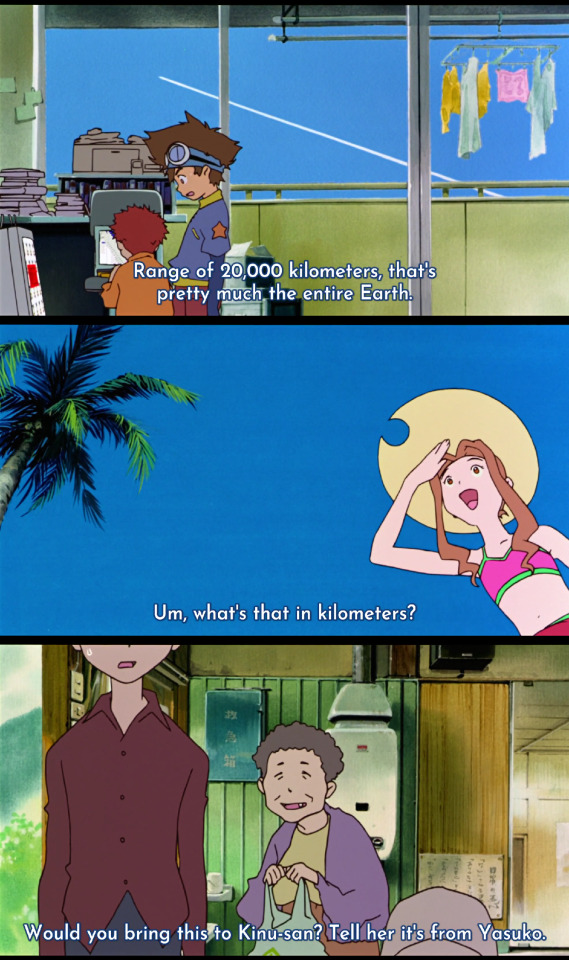
Taichi: Y-You're messing with me.... Koushiro: The nuclear missile is called One-Shot Peacekeeper. Range of 20,000 km, which is nearly the entire Earth. Top speed is 15,000 mph. Taichi: ...what's that in kmph? Koushiro: In parentheses, "Mach 23". Taichi: T... Twenty-three...?
The Earth is a little over 40,000 km in circumference so Koushiro's math checks out. Depending on which direction you shoot in, you can cover almost everything on the planet with that kind of range.
Additionally, the speed required to achieve orbital velocity is about 17,500 mph. So this missile can't reach orbit, but it's close.
As Koushiro says that, we cut to Mimi in Hawaii watching the "jet" suddenly streak by overhead. Seems to be heading westward from the continental U.S.
Mimi: Oooooo!
She has no idea what she's looking at. It's probably just a cool plane going super fast in the air.
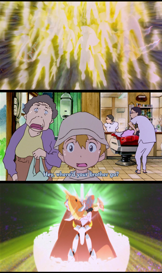
Koushiro: But we don't know what its target is or where it is in the air right now. Only that it's going to detonate somewhere in the world... in nine minutes.
Meanwhile, in Shimane, the people in the barbershop have no idea. The elderly couple discuss dark clouds moving in over the region.
Elderly Man: It's getting cloudy. Elderly Woman: So quiet, though. I should probably go bring in the laundry right away. Elderly Man: Right away!
The old woman offers Yamato a grocery bag.
Elderly Woman: Would you bring these things to Kinu-san? Tell her they're from Yasuko. Yamato: ... Yasuko: Huh? Are you even listening?
They are not. Yamato and Takeru stare at the computer screen, paralyzed with terror by the reality in front of them.
An interesting note is that it's only one missile. Diablomon isn't going Full Skynet and trying to annihilate humankind. It only has one target it intends to utterly destroy.
In the dub:
Tai: But the military has the power to stop it, right? Izzy: Every country is trying to intercept them, including Japan. But Diaboromon has infiltrated all the computers and is rerouting them to fall harmlessly in the ocean near Hawaii! Mimi: (Hawaii) Ooooo, fireworks! Izzy: I've got the trajectory for the other missile. Let me calculate. ...carry the two, times three... TAI, IT'S AIMED RIGHT FOR THIS NEIGHBORHOOD!!! Tai: (frustrated) Ugh....
SPOILERS, IZZY. FUCK. I mean, I think most people already guessed that, but still.
Following Tai's incredibly understated groan, the Shimane scene is cut.
When Izzy says Diaboromon is "rerouting them to fall harmlessly in the ocean", the wording here is a little confusing. I think he means that Diaboromon's sending every country's counter-missiles to Hawaii? But the way he words it makes it sound like he's sending the two nukes to Hawaii.
It's a bit of a word salad to try and justify why Mimi's seeing a missile streak by in Hawaii. Which... is kind of a fair question, because Hawaii isn't between the continental U.S. and Japan. It's pretty far south, between Mexico and the Philippines. So I have no idea why the missile passed directly over Mimi's head.
(It heard how cool she was and wanted to swing by to see for itself. It has more than enough range for a detour.
Back at Taichi's home, more emails come in.
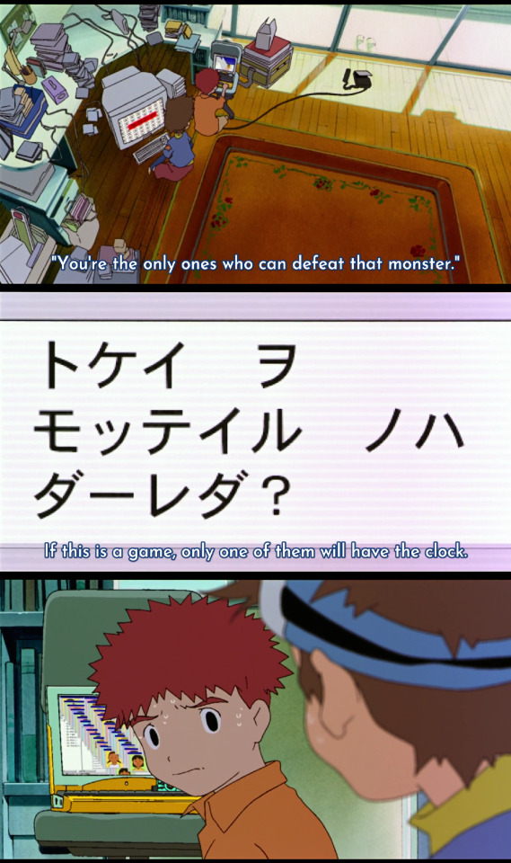
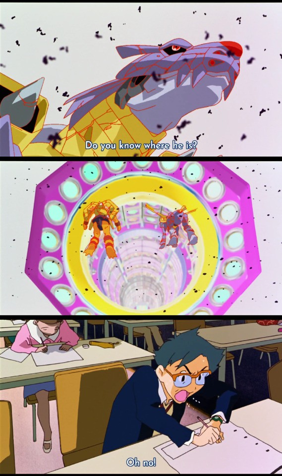
Koushiro: This email's from Indonesia: "You must defeat the enemy somehow." Over here, from Armenia: "You're the only ones who can defeat that monster." From Qatar: "Please ganbatte." Taichi: We should ganbaru...
Watching the screen, they're now up to 64 Diablomon and still dividing.
Taichi: But we can't defeat all of them! Koushiro: A nuclear missile can't detonate unless the fuse is activated. If this is supposed to be a game, then which one of those things has the clock? Defeat that one and the fuse won't activate. Taichi: But how do we find that one? Koushiro: That is... We'll have to defeat them one by one. Taichi: But that will take too long!
Koushiro slowly turns around to face Taichi, so Taichi can see how serious he is.
Koushiro: But that's the only choice we have. Taichi: (stunned) ....
Taichi is left speechless by how dire their predicament is.
In the dub... the hack and slash job continues. The scene continues, but they don't use the footage for it. Instead, remember that bit they cut out where Taichi cries "WE'RE SCREWED!" and falls over? Yeah, they past that part in for the footage of this section.
Izzy: Tai, look! Emails from all over the world! "Get that evil Digimon! You're our only hope!" Here's another one: "Be home by six o'clock!" ...oh, wait, that's from my mom. Tai: I'M TRYING TO SAVE THE WORLD AND YOU'RE READING FANMAIL!!! Izzy: WE JUST LOST OUR CONNECTION!!! Tai: (falls over comically) Greeeeeeeeat. Izzy: Don't worry, I'll get it back! Listen, I think if we defeat the original Diaboromon, the rest will disappear. Tai: (gets back up, excited) WHAT!?!? Izzy: All we have to do is destroy each one until we've found the original.
They then use a shot of the "jet" flying in the sky to reset the positions of the characters and join back up with the original footage at "But that will take too long!"
Tai: Sounds great! How many are there so far? Izzy: Oh no.... (Izzy slowly turns around) Tai: Spit it out, Izzy! How many are there! Izzy: ...there are over 75,000 and counting. Tai: (stunned) ...
In addition to the hack and slash job, we are now wildly off-script.
They keep the basic idea that there is one specific Diablomon we must defeat. But the relationship between that Diablomon, the detonation of the nuke, and the little clock Diablomon showed the camera earlier? Completely wiped off the board.
Along with it goes the characterization that Diablomon is still, even in this form, playing games.
In its place, we get the connection going out for like half a second, which adds nothing to this scene. That's clearly there because they cut out this comical footage of Taichi falling over earlier and wanted to use it somewhere.
And the dub also claims that there are now 75,000 Diaboromon. We're at like 64 or so. The Americans inflated the hell out of these numbers.
While Taichi struggles to process this situation, WarGreymon suddenly reaches out.
WarGreymon: Taichi.... Taichi: .... WarGreymon: Taichi...! Taichi: .... WarGreymon: Taichi! Taichi: (gasp)
That shakes him out of it, and he returns his attention to the screen. The Ultimate Digimon begin to move, ready to go once again despite their injuries and damaged armor.
WarGreymon: Taichi... Pull yourself together, Taichi, and let us handle this. Taichi: WarGreymon.... MetalGarurumon: Do we know where it is? Yamato: MetalGarurumon.... Koushiro: Guys.... (steeling himself) I'm sending the address now! MetalGarurumon: Please.
An exit from their current server appears, and the pair of Ultimates exit into the internet once more.
Taichi: (quietly) You're right. It's the only way. I'm sorry. Koushiro: (quietly) Yeah....
Meanwhile, in the kitchen, Yuuko checks on her cake.
Yuuko: Seven minutes left!
Across Tokyo, Jou scrambles to finish his entrance exam.
Announcement: Seven minutes left! Jou: (writes frantically) OH NO!!!
Seven minutes left!
Yuuko's cake provides a curious timeframe. It's been twenty-three minutes since she put it into the microwave, and the nuke was fired thirty-three minutes ago. This means the nuke was launched ten minutes before Yuuko put the cake in the oven. Ten minutes before the fight with Infermon, ending in Infermon using the NTT system to shut Taichi and Koushiro out of the internet.
The timeframe is honestly fascinating, as it implies that the nuke was one of the numerous errors that emerged during Kuramon's hatching. Like when Jou missed his train because the doors wouldn't open. The nuke was fired then, during the opening credit sequence, and has been in the air this entire time.
In the dub:
WarGreymon: Tai.... Izzy: What's that? It didn't sound like my stomach. WarGreymon: Tai! Tai: Ah! (Tai returns his attention to the computer) WarGreymon: Have faith! I'll find... the original! Tai: WarGreymon.... MetalGarurumon: Mrrrgh... I'll help you.... Matt: MetalGarurumon! Izzy: They're so slow.... It's because of all the emails! They're slowing down our Digimon's processing speed! I've gotta write to everybody and tell them to stop emailing us until the Digimon are back to full strength! Tai: Are you crazy, Izzy!? Do you know how long that will take!? There's no time! Now we're-- (Cut to Yuuko) Yuuko: --just about-- (Cut to Joe) Announcer: --FINISHED!!! Joe: (writes frantically) IT CAN'T END LIKE THIS!!!
Love what the dub does with those Yuuko and Jou cuts. Beautiful.
So here we get the explanation for all the "WarGreymon is slowing down for some reason!" stuff. The emails coming in are screwing with his and MetalGarurumon's processing speed.
This is actually a plot point from the original. The dub went ahead and introduced it way earlier so they could build up to it. And use it to explain that weird moment when WarGreymon suddenly froze up after Taichi disconnected. Good call. A+
Seven minutes left!
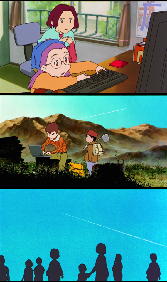
As WarGreymon and MetalGarurumon fly through the internet, more and more emails come in... including a couple of fairly significant cameos.
One is a certain little girl with purple hair that we'll be getting to know better next season.
Another is a boy named Ryo Akiyama. Ryo is the main playable character for a series of Adventure-adjacent video games that take place in the margins around the anime's continuity. We'll be seeing him cross over more and more into the anime proper with not only the next season of Adventure, but also Digimon Tamers.
Despite Tamers being in a separate continuity. It's weird.
Koushiro: There's so much email flowing in.... "Ganbare WarGreymon" from Costa Rica. "Don't lose this, MetalGarurumon," from the Philippines. Takeru: (gripping Yamato's shirt) Onii-chan... Don't give in.... Yamato: I won't give up... not to the very end. Taichi: I will never give up....
As the boys steel their resolve, the clock ticks down.
The dub plays a snippet of Here We Go by Jason Gochin here for a rock interlude. They snip out Koushiro's dialogue about the email, though they still use the footage so we see his lips move silently.
T.K.: Tell me... Will they make it...? Matt: I'm not sure, T.K. But they're gonna try. Tai: Don't give up, guys. No matter what happens, don't give up!
An interesting note is that the dub treats Tai and Matt as passive observers here while the original treats them as active participants. This is because they may not be the ones throwing the punches but it's their power that WarGreymon and MetalGarurumon are wielding.
Six and a half minutes left!
WarGreymon and MetalGarurumon arrive in an area that has been completely overrun with the growing Diablomon swarm.
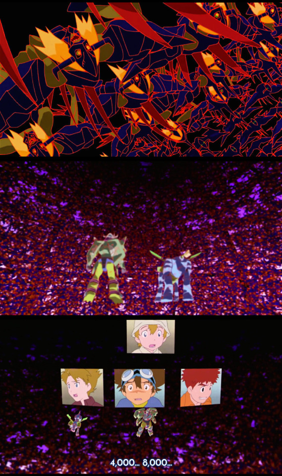
Yamato: They're... How many of them are there? Koushiro: 4,000... 8,000... It copied itself again! 16,000! They keep making more!
In the dub, the Diablomon are uttering a chorus of "Don't interfere!" over and over and over again. Presumably referring to his plan to drop a nuke on Willis.
Matt: How many copies of Diaboromon are there now!? Izzy: To be honest, I don't know. I stopped keeping track a while ago. It's gotta be well over a million!
It is not. No reason not to use the original numbers; Dub team's scrawling in some extra zeros for American machismo.
No time to get our bearings. At once, thousands of Diablomon open fire on our boys.
WarGreymon and MetalGarurumon are forced to try and weave through the barrage of incoming shots. They don't last long. MetalGarurumon is the first to start taking hits.
Yamato: Ah! Taichi: MetalGarurumon!
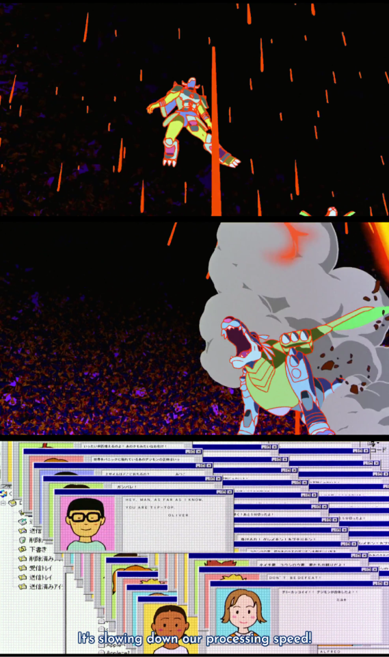
While Taichi's eyes are on MetalGarurumon, several shots catch up to WarGreymon, pummeling him as well.
Taichi: Ah! Takeru: They're moving really weird! Koushiro: It's because of all these emails flooding in from around the world! Having so many emails come in is slowing down our processing speed! Takeru: If this keeps up, we'll lose! Koushiro: (typing frantically) To everyone around the world: WarGreymon and MetalGarurumon's responsiveness is dropping! I'm begging you to stop sending emails!
Anyone who's seen a thousand-strong office "Please stop Replying All" chain knows that ain't gonna cut it.
In the dub:
(MetalGarurumon is hit) Matt: Ah! Tai: METALGARURUMON!!! (WarGreymon is hit) Tai: Ah! T.K.: WarGreymon has started to slow down again! Izzy: It's the emails! They're coming in faster than ever! They're slowing down the processing speed even more! Tai: They're sitting ducks out there! Izzy: (typing frantically) Please, guys, stop writing! I know your intentions are good but you're really hurting our cause! Your emails are putting our Digimon in danger!
The dub seems to think the emails are only affecting WarGreymon. They may have gotten confused over the -tachi suffix. WarGreymon-tachi is being affected.
The -tachi suffix is how you pluralize a group of people in Japanese. When stuck to a name, it basically means, "and others in their group" using only two syllables. In this case, MetalGarurumon is the -tachi.
Despite Koushiro's best efforts, the damage is done. WarGreymon and MetalGarurumon float unmoving in the void once the barrage of enemy fire lets up.
Taichi: WARGREYMON!!!
Letting out slow, hollow breathes, Taichi slowly reaches for the screen. Reaches for his partner. Drawing closer and closer and--
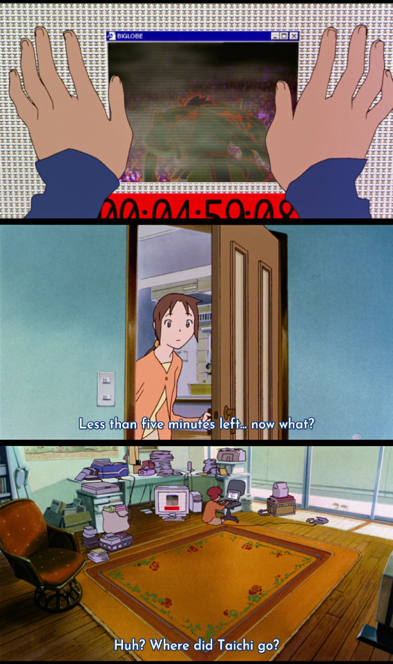
Yuuko: (opens door) Koushiro-kun, will you be eating lunch with us? Koushiro: (doesn't notice; mutters) It's useless. I can't stop these emails. There's only five minutes left... What do we do? Yuuko: (smiling) I'm sorry for disturbing you.
Yuuko quietly closes the door. Then, suddenly, she opens it again.
Yuuko: Huh? Where did Taichi go?
A shot of the room reveals that, indeed, Taichi is gone. Koushiro is alone in Susumu's office.
In the dub:
Tai: (gasp) WarGreymon...!
In the original, the music is silent here. The only sound we hear is the echoing of Taichi's hollow, ragged breaths. The dub adds this incredibly loud, eerie background music that drowns out both Tai's breathing and also the new dialogue they gave him.
Tai: WarGreymon... I've got to help... There must be a way... Somehow.... (Yuuko enters) Yuuko: More juice, Izzy? I just squeezed some onions! Izzy: No thanks! I'm rerouting incoming data from the remote server into local memory. Yuuko: (clearly did not understand that) Oh. Whoops. I'll just leave you two alone. (Yuuko departs, then comes back in) Yuuko: Wait a minute! Where did Tai go?
Koushiro is both freaking out and hyperfocused to the point that he notices neither Yuuko entering the room nor Taichi's mysterious exit from it. It's an established character trait that he sometimes doesn't notice other people when he's hyperfocused.
(It got him thrown off a cliff once. By me.)
But Izzy has the presence of mind to briefly chat with Yuuko.
So, where did Taichi go? Into the computer, of course.
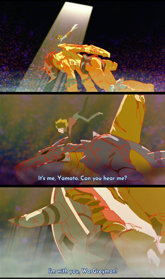
That big square window that the children appear in during all these fights? Taichi passes through his to enter the internet and reach WarGreymon.
He slowly descends until he reaches WarGreymon.
Taichi: WarGreymon! WarGreymon: ...
Some distance away, Yamato does the same. He passes through his light window and enters, floating down to MetalGarurumon.
Yamato: Metal... MetalGarurumon! It's me, Yamato. Can you hear me? Open your eyes! Taichi: Yamato....
Taichi watches Yamato for a moment, then does the same thing.
Taichi: I'm here! I'm here too! I came so we can fight together! WarGreymon: ... Taichi: You... You don't have to fight alone anymore.... WarGreymon: ... Taichi: I'm right here! I'm here with you, WarGreymon!
I love how the screens are angled to create the imagery of the children descending upon the near-dead Digimon like angels from heaven. I see what you did there.
In the dub, Kari's voice-over pops back up to try and explain this.
Kari (V.O.): None of us are sure how, but Tai's bond with WarGreymon was so strong that Tai himself became digital!
"None of us are sure how." Kari, go have some more birthday cake. You weren't even here for this.
This is neither the first nor the last time a Chosen Child's holy light will open a gateway between realities.
Tai: WarGreymon... I'm here.... (Matt descends from the other screen) Matt: MetalGarurumon! Wake up! Don't quit now! Why won't he answer me, Tai? Tai: Keep trying, Matt! (Tai looks down at WarGreymon) Tai: Listen. I don't have a whistle to wake you, but I want you to know you're not alone, okay? WarGreymon: ... Tai: And the mail keeps coming! It won't stop! WarGreymon: ... Tai: Kids from all over the world are writing to you. They need your help. You're the only one who can do it! Feel their hope! Feel their strength!
"I don't have a whistle to wake you" is a reference to Kari's whistle being used to wake Greymon in the first OVA's battle with Parrotmon. Since the OVA formed the first portion of Digimon: The Movie, they reference its events here.
Taichi's speech to WarGreymon is personal and focused on their bond with one another. Tai's speech is about how much the entire world loves WarGreymon, which does segue pretty well into this next bit.
WarGreymon: ...u...urgh....
In the dub:
WarGreymon: ...I feel them!
WarGreymon's body shakes slightly. He doesn't open his eyes; Instead, the holy light glows from within the eyeholes of his helmet.
All around them, a wall of emails appears, forming a barrier between them and the Diablomon swarm. WarGreymon and MetalGarurumon don't come to, but instead seem to vibrate and jitter.
Then WarGreymon disintegrates into data, which collects and pours inside his helmet. The same happens to MetalGarurumon.
Through those email boxes, holy light from all of the kids watching gathers, entering the data space in the glowing silhouette of each child. They collect, pooling into energy between the twin helmets of WarGreymon and MetalGarurumon.
Meanwhile, at the barber shop:
Barber: (suspiciously) Hang on, where did your brother go!?
The barber looks around for Yamato. Poor Yasuko, on the other hand, just watched a preteen boy phase inside of a computer screen and looks like she's about to have a heart attack.
Takeru: He's here.....
The energy forms the shape of an egg made of pixels, which then slowly peels back to reveal a new Digimon inside.
Koushiro: WarGreymon and... Takeru: ...MetalGarurumon... Koushiro: ...combined!
The technical term is Jogress Evolution. Jogress is a mechanic from the V-Pet that hasn't yet appeared in the anime, in which two Digimon fuse together to form a Perfect or Ultimate Digimon. Many of the Digimon we've seen throughout the anime could only be achieved through Jogress in the original V-Pets, such as Piemon or WereGarurumon.
The arrival of Omegamon, or Omnimon in the dub, marks the first time this mechanic has been brought into the show. We'll be seeing more of it in Adventure 02.
(The only reason Takeru and Hikari don't have a Jogress with each other is because EnbyAngemon would be so game-wreckingly badass that no villain could ever match them.
Or, more realistically, because predominately heteronormative writers often struggle with the idea of two characters from opposite sexes doing a Fusion. Their eyes bug out and they bluescreen while muttering, "But how would that even....")
The dub crops the barbershop to cut the barber out, though his reflection remains visible in the mirror, but leave Yasuko's stunned face. This is despite the fact that they cut the setup scene for this gag, with Yasuko saying goodbye to Yamato and Takeru.
Barber: Where'd you brother go!? Hjbyhjbyhjby....
They play the barber as freaked out and melting down. In the original, like Yuuko, he didn't see the disappearance happen (but Yasuko did). He just... doesn't trust these random kids to be unsupervised in his shop, and really doesn't like the fact that one stray child is now unaccounted for.
T.K.: They combined! (Omnimon is revealed) Izzy: Part WarGreymon.... T.K.: Part MetalGarurumon.... Izzy: They Digivolved together to become-- Omnimon: OMNIMON!!!
It's nice of Omnimon to introduce himself since we don't have rundowns to tell us about him. For the record, his signature weapons on his arms made from the helmets of his component Digimon are called the Garuru Cannon and Grey Sword. "Cannon" and "Sword" being the English words themselves, as usual.
With Taichi and Yamato perched on his shoulders, Omegamon is born.
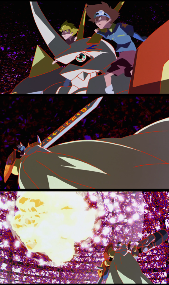
The swarm opens fire immediately. Drawing his Grey Sword, Omegamon deflects all of their shots into a line of Diablomon, annihilating a huge chunk.
Koushiro: Amazing!
Koushiro hasn't seen anything yet. With his Garuru Cannon, unloads shot after shot into the enemy ranks. Each blast wipes out a huge chunk of the Diablomon swarm.
The dub uses this as an opportunity for another musical interlude, playing Let's Kick It Up by Paul Christian Gordon over the carnage. They also have Omnimon call these attacks, naming them Transcendent Sword and Supreme Cannon.
Only one Diablomon remains standing when Omegamon's done.
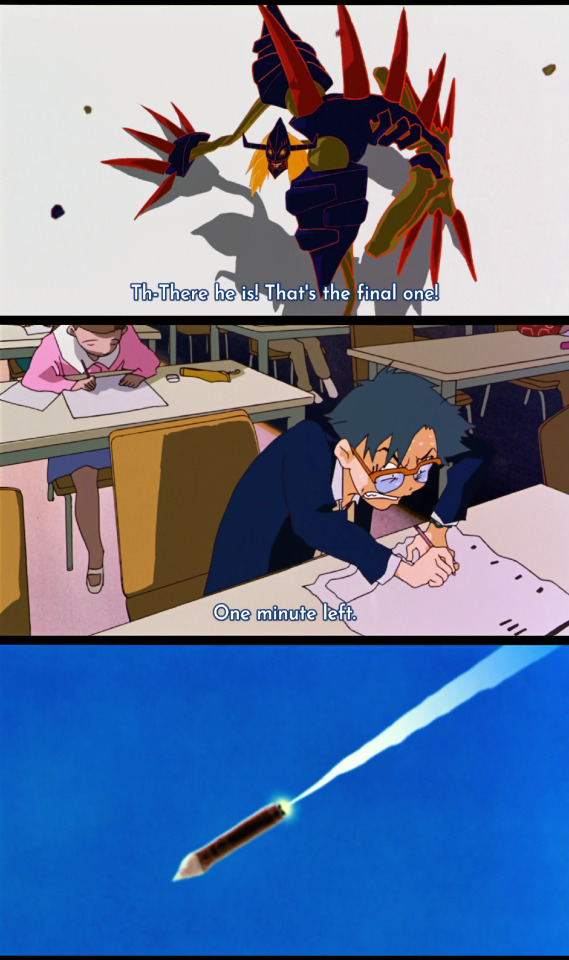
Koushiro: Right there! That's the last one! That one has the clock!
Awfully inconvenient that the one with the clock just so happens to be the only one who survived Omegamon's bombardment.
Diablomon starts moving quickly around the room, making evasive maneuvers to try and run down the clock. Every time Omegamon turns around and aims at it, it darts away again.
Taichi: It's not here! Koushiro: WE HAVE LESS THAN A MINUTE!!!
Cut to Jou desperately trying to finish his exam.
Jou: ONE MINUTE LEFT!!!
And Yuuko watching her cake cook.
Yuuko: (cheerful) One minute left!
Finally, we cut up to the "jet" in the sky... which turns out to actually just be a jet, as another much faster object enters the airspace, criss-crossing its contrail with the jet's. Closer inspection of the new object reveals it to, in fact, be the One-Shot Peacekeeper missile approaching Odaiba.
This, I should note, is the first we learn of its destination in the original. No one knew where it was in the air or where it was going to land.
In the dub:
Izzy: Tai, there's the original! Get him! We're running out of time! Tai: Omnimon, quick! Attack!
Awfully inconvenient that the original just so happens to be the only one who survived Omnimon's bombardment.
Like, they changed the plot mechanics behind this fight but this is still a glaring contrivance. XD You could have left it at "We have to destroy every last one" if you wanted to patch this.
Tai: Where is he!? (Diaboromon dodges more) Tai: One minute to go! (Cut to Joe) Joe: ONE MINUTE TO GO!!! (Cut to Yuuko) Yuuko: (cheerful) One minute to go!
Tai calls out the time remaining here rather than Izzy, even though he can't see the clock from here.
As the missile's coming in, the dub also adds some dialogue from some military guys.
Soldier: Squad leader to command: We were unable to destroy the target. The missile will impact. Repeat, the missile will impact!
This ties in with the added detail from earlier, that every nation in the world is attempting to intercept the nuke and failing.
Inside the battlefield, the last Diablomon is still moving too fast for Omegamon to get a bead on it.
Takeru: Onii-chan! You have to find it quick! There's no time left! ONII-CHAN!!! HURRY!!!
45 seconds left on the clock. Koushiro works the problem in his head.
Koushiro: Its speed is too high. At this rate, even with tremendous power, we're going to lose due to the difference in reaction time. What can we do?
Thirty seconds left. Cutting over to the barber shop for a moment, we see that Yasuko's husband has popped over to watch the screen too. No explanation is offered.
(I guess he wants to find out what all the commotion is about? Yamato fucked off all of a sudden and Takeru is shrieking at the computer like it's the end of the world. I'd be curious too.)
Takeru: THIRTY SECONDS LEFT!!! Koushiro: (gasp) That's it....
Koushiro looks at all the incoming emails on his laptop.
Koushiro: A transfer! I can forward all of this email to that thing's address!
Koushiro quickly types in the current address that Diablomon is at, presumably the FactoryMark server we last saw it at.
Koushiro: GO!!! (click)
Koushiro dramatically presses the Enter key. Inside the battleground, Diablomon lands on the wall and prepares to make its next move, but then stalls all of a sudden. It struggles, shaking in place, but can't move. A little Windows hourglass appears over it; the loading symbol for computers from that time.
In the dub:
Tai: He keeps moving! Every time we get him in our sights, he jumps somewhere else! He's too fast for us! (45 seconds remain) Izzy: We have the power to destroy him now, but we don't have the time. Willis was right; We have to find some way to slow down Diaboromon.
...Willis said that after the first fight with Infermon. That he foresaw this exact predicament that far in advance is fucking wild.
T.K.: THIRTY SECONDS LEFT!!! Izzy: (gasp) The emails! If I forward him all the emails, it will slow him down just like it did us! Keep sending them, kids! (Izzy prepares to forward) Izzy: YOU!!! GOT!!! MAIL!!! (click)
Using "You got mail" as a battle cry here is pretty fucking sweet. For those too young to remember, an early form of internet was AOL which had a robot voice chime "You got mail" whenever you received an email.
With ten seconds remaining on the clock, Omegamon moves in for the kill.
Koushiro: Ten seconds left!
Koushiro counts down the seconds while Omegamon moves in. A brief cut of the barbershop shows that now everybody's paying attention to what's happening on the computer screen. Even the barber.
At one second, the attack lands. Omegamon drives his Grey Sword through Diablomon's skull.
At the same time, Yuuko's cake is finished! She takes it out of the microwave to find it grotesquely burnt.
Yuuko: Ah!? It's ruined! That's so weird. It should be controlled by the microcomputer....
COMPUTER YOU SAY
One last bug for the road. Diablomon ruined Yuuko's cake.
Outside, time's up. The nuclear missile crashes into the Tokyo Bay. We briefly see Sora in her room. With Diablomon dead, Taichi's email finally makes it through to her.
In the dub:
Tai: TEN SECONDS LEFT!!!
Again, despite not being able to see the clock, Tai is the one who counts down the seconds in the dub rather than Izzy.
(Omnimon stabs Diaboromon in the head) Diaboromon: Connection... Terminated....
The dub not only gives Diaboromon a line upon being stabbed, but rearranges scenes. Two upcoming shots get moved up to here. The first is of Diaboromon's face melting away to reveal the stabbed clock. The second is the timer stalling out and flickering between 00:01 and 00:02.
This serves to assure the audience that we got it, we stopped the detonation, earlier than in the original. The original keeps the tension ratcheted up as the missile lands, with it not yet clear if we killed Diablomon fast enough.
Yuuko: (ruined cake) Ugh, lousy microwave. How come every electronic appliance has to have a bug in it!? (Missile crashes into the bay) Sora: (email arrives) Huh? It's about time!
I mean. By Dub Yuuko's own admission, this was the first time she ever used flour to make a cake. It's just as likely that she's the culprit here as it is the microwave. :P
As the missile lands, Koushiro sprints out onto the balcony, distraught.
Koushiro: We didn't make it in time!
Cut to the internet battlefield. Diablomon's face melts away, revealing the clock pierced by Omegamon's blade. The timer stalls out, flickering between 00:01 and 00:02.
Meanwhile, Sora reads Taichi's message and notices the little heart he accidentally added when Hikari startled him. She's touched.
Sora: Ehehe... (affectionately) Stupid Taichi....
Success! Taichi accidentally fluked his way into forgiveness!
Out by the bay, people gather to look at the undetonated nuclear missile. It tips over due to its weight and falls flat into the water.
Up on the balcony, Koushiro breathes a sigh of relief.
Koushiro: (exhausted) We... We... We.... Taichi: (exhausted, also on balcony now) We made it in time!
Which is where the OVA ends! Abruptly! On Taichi quite reasonably looking like he's about to cry and then pass out. What did you do for your spring break, kids? Oh, I thwarted nuclear motherfucking Armageddon.
There is an epilogue of sorts in the form of ending slides in the credits. We'll address that in another post.
In the dub, this final sequence plays out with The Impression That I Get from The Mighty Mighty Bosstones playing in the background. Sora reads Tai's English email.
Sora: (reading aloud) Dear Sora, I'm sorry I threw up, hat, so what's a few raindrops between friends, love Tai. ...aww... (affectionately) Stupid Tai.... (Missile tips over into the water) Izzy: (exhausted) I'm... about... to barf.... Tai: (exhausted) Wait 'til you try the cake....
The dub closes on one last Yuuko cooking joke. To be fair, the cake legitimately did come out horribly. :P
There will be no epilogue slides for the dub, because it segues into the third part of Digimon: The Movie from here. We'll talk about that when we get to Hurricane Touchdown.
17 notes
·
View notes
Text
A recently developed block copolymer could help push the limits of integration and miniaturization in semiconductor manufacturing, report scientists in Tokyo Tech and TOK. Chemically tailored for reliable directed self-assembly, the proposed compound can arrange itself into perpendicular lamellar structures whose half-pitch width is less than 10 nanometers, outperforming conventional and widely used block copolymers. Miniaturization is one of the fundamental qualities of modern electronics and is largely responsible for the incredible increments in performance witnessed over the past decades. To keep this momentum going, it is necessary to achieve circuit patterns finer than the existing ones on semiconductor chips, which are a crucial part of all electronic devices. Some experts estimate that, by 2037, the smallest distance between features in semiconductor devices, known as 'half-pitch,' will need to be as small as 8 nm to support next-generation electronics, emphasizing the need for advancements in lithographic processes (method of creating highly complex circuit patterns on semiconductor parts).
Read more.
#Materials Science#Science#Block copolymers#Polymers#Semiconductors#Manufacturing#Self assembly#Tokyo Institute of Technology
13 notes
·
View notes
Text
1 note
·
View note
Text
#Outsourced Semiconductor Assembly and Test Services Market Size#Outsourced Semiconductor Assembly and Test Services Market Share#Outsourced Semiconductor Assembly and Test Services Market Growth#Outsourced Semiconductor Assembly and Test Services Market Trends#Outsourced Semiconductor Assembly and Test Services Market Forecast Analysis#Outsourced Semiconductor Assembly and Test Services Market Segmentation#Outsourced Semiconductor Assembly and Test Services Market 2024#Outsourced Semiconductor Assembly and Test Services Market CAGR#Outsourced Semiconductor Assembly and Test Services Market Analyzer Industry
0 notes
Text
Semiconductor Assembly and Packaging Services Market Size, Share, Industry Analysis and Forecast 2024-2032
Semiconductor assembly and packaging services are crucial components in the semiconductor manufacturing process, transforming raw semiconductor dies into finished products ready for integration into electronic devices. This phase involves a series of intricate processes, including die attachment, wire bonding, encapsulation, and testing. As the semiconductor industry evolves to meet the growing demands of technology, the importance of advanced assembly and packaging solutions has never been greater.
The assembly and packaging processes are essential for protecting semiconductor devices from environmental factors and mechanical stresses while ensuring optimal performance. With the increasing complexity of semiconductor designs, manufacturers are investing in innovative packaging technologies, such as system-in-package (SiP) and 3D packaging, to accommodate high-density applications. These advancements enable more compact and efficient designs, paving the way for the next generation of electronics.
The Semiconductor Assembly and Packaging Services Market is witnessing growth as demand for advanced packaging solutions increases, enabling miniaturization and improved performance in a wide range of electronic devices.
Future Scope
The future of semiconductor assembly and packaging services is promising, driven by the demand for more sophisticated semiconductor devices across various sectors. As technology trends like 5G, artificial intelligence (AI), and the Internet of Things (IoT) continue to expand, the need for high-performance packaging solutions will increase. Manufacturers will require assembly services that can handle complex geometries and multilayer designs, ensuring reliability and functionality in compact spaces.
Additionally, the push for sustainability in manufacturing practices will influence the development of eco-friendly packaging materials and processes. As environmental regulations tighten, companies will seek out assembly and packaging solutions that minimize waste and reduce the carbon footprint. The adoption of recyclable materials and innovative packaging designs will become integral to meeting these sustainability goals.
Trends
Several key trends are shaping the semiconductor assembly and packaging services market. One significant trend is the increasing focus on advanced packaging techniques, such as fan-out wafer-level packaging (FOWLP) and chip-on-wafer (CoW) technology. These methods allow for improved thermal performance, reduced signal loss, and greater integration density, addressing the needs of modern electronic applications.
Another trend is the growing demand for automation and smart manufacturing in assembly processes. Companies are leveraging automation technologies to streamline operations, reduce labor costs, and enhance precision in assembly tasks. This shift towards smart manufacturing is crucial for improving yield and efficiency in the assembly and packaging stages.
Application
Semiconductor assembly and packaging services are utilized across various industries, including consumer electronics, automotive, telecommunications, and industrial applications. In consumer electronics, these services ensure that devices such as smartphones, tablets, and wearables are compact, durable, and capable of high performance. Advanced packaging solutions enhance the functionality and reliability of these devices in a highly competitive market.
In the automotive sector, assembly and packaging services play a vital role in producing components for advanced driver-assistance systems (ADAS), power management systems, and infotainment solutions. As vehicles become more connected and automated, the reliability of semiconductor components is paramount for safety and performance.
Telecommunications is another key application area, where assembly and packaging services are essential for manufacturing components used in network infrastructure, including routers, base stations, and switches. The increasing demand for higher data rates and lower latency in communication networks drives the need for advanced packaging solutions that can support these requirements.
Key Points
Transform semiconductor dies into finished products ready for electronic devices.
Driven by the demand for advanced technologies and sophisticated packaging solutions.
Promising future with growth opportunities in sustainability and eco-friendly practices.
Trends include advanced packaging techniques and automation in assembly processes.
Applied across consumer electronics, automotive, telecommunications, and industrial sectors.
Read More Details: https://www.snsinsider.com/reports/semiconductor-assembly-and-packaging-services-market-4537
Contact Us:
Akash Anand — Head of Business Development & Strategy
Email: [email protected]
Phone: +1–415–230–0044 (US) | +91–7798602273 (IND)
0 notes
Text

Nature-inspired solar lasers could sustainably power space missions
International scientists, including a team from Heriot-Watt University, has announced plans to develop a revolutionary new way of harvesting solar energy in space.
The new technology would directly convert sunlight into laser beams, facilitating the transmission of power over vast distances, such as between satellites, from satellites to lunar bases, or even back to Earth. The approach is inspired by the way bacteria and other plants and organisms convert light energy into chemical energy—a process known as photosynthesis. Repurposing natural photosynthetic structures from nature will form a key component in the new laser technology.
If successful, their innovative technology could help global space agencies to power future endeavors such as lunar bases or missions to Mars, as well as open new pathways for terrestrial wireless power transmission and sustainable energy solutions globally.
The APACE project brings together researchers from the U.K., Italy, Germany and Poland to create the new type of solar-powered lasers, which will provide reliable, efficient power for the growing number of satellites and future space missions.
The system will repurpose light harvesting antennas of certain photosynthetic bacteria, which are highly efficient at absorbing ambient solar light and channeling its energy to a desired target location as part of their photosynthetic cycle.
The team plans to realize their idea under laboratory conditions first, before testing and refining its suitability for deployment into the space environment.
The researchers will begin by extracting and studying the natural light-harvesting machinery from specific types of bacteria that have evolved to survive in extremely low light conditions. These bacteria have specialized molecular antenna structures that can capture and channel almost every photon of light they receive—making them nature's most efficient solar collectors.
In parallel, the team will develop artificial versions of these structures and new laser materials that can work with both natural and artificial light-harvesters. These components will then be combined into a new type of laser material and tested in increasingly larger systems.
Unlike conventional semiconductor solar panels, which convert sunlight into electricity, their bio-inspired system builds on a sustainable organic platform with the potential for replication in space. It would then allow for the direct distribution of power without relying on an electric intermediary.
Professor Erik Gauger from the Institute of Photonics and Quantum Sciences at Heriot-Watt University is leading the theoretical modeling aspects of the project.
He explains, "Sustainable generation of power in space, without relying on perishable components sent from Earth represents a big challenge. Yet, living organisms are experts at being self-sufficient and harnessing self-assembly. Our project not only takes biological inspiration but goes one step beyond by piggybacking on functionality that already exists in the photosynthetic machinery of bacteria to achieve a breakthrough in space power.
"Our APACE project aims to create a new type of laser powered by sunlight. Regular sunlight is usually too weak to power a laser directly, but these special bacteria are incredibly efficient at collecting and channeling sunlight through their intricately designed light harvesting structures, which can effectively amplify the energy flux from sunlight to the reaction center by several orders of magnitude. Our project will make use of this level of amplification to convert sunlight into a laser beam without relying on electrical components.
"We already know it is possible to grow bacteria in space, for example through studies on the International Space Station. Some tough bacteria have even survived exposure to open space! If our new technology can be built and used on space stations, it could help to generate power locally and even offer a route to sending power to satellites or back to Earth using infrared laser beams.
"This technology has the potential to revolutionize how we power space operations, making exploration more sustainable while also advancing clean energy technology here on Earth. All major space agencies have lunar or Mars missions in their plans and we hope to help power them."
The research team expects to have its first prototype ready for testing within three years.
7 notes
·
View notes
Text
Chapter 205 Trivia
How does a baby, with their chubby little fingers, snap them? Ryusui was obviously gifted with strong, dexterous fingers from a young age…
The flashback makes it seem like Ryusui is remembering the event, however: babies start walking between 6-18 months and Ryusui is being carried, speaking clearly is 12+ months, and memories like this one would only start from around 2-3 years onward.
Thus, this isn't Ryusui's memory.
(He was probably told about it, however remembering the 20 digit number as part of a memory is pretty impressive…)

Speaking of, well, speaking: baby Ryusui sure learnt the word "desire" quickly, however pronunciation is harder. The baby speech is present in both languages, with the Japanese version saying "欲ちい"(hochī) rather than "欲しい" (hoshī).

If we assume Ryusui is about 1 year old here for the reasons I listed above, that means that Sai is only 3 years older.
Because of Ryusui's various petrifications, Ryusui's aged about 3 years over that time.
I'm not sure who's the older brother now…

Everyone's mental math methods shown here are references to the chapter 18 bonus story, when Chrome and Senku had the arithme-battle.
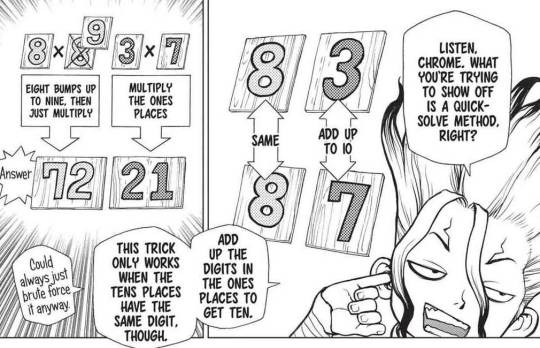
Ryusui's fangs seem a lot more prominent this chapter, I guess he's really sinking his teeth into getting Sai on board with their plan!

This man here is Ryusui's uncle, who's been shown in a few flashbacks before. Where Ryusui and Sai's parents are is anyone's guess.


The game character is wielding a gun and a sword, and wearing an outfit that looks like Ryusui's.
Or is Ryusui wearing an outfit that looks like the game character's..? 🤔
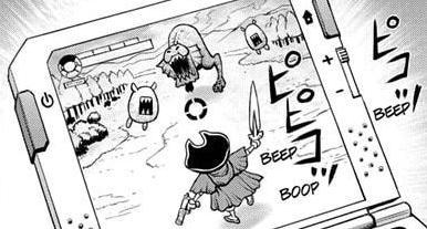
The airplane Sai takes is based on a Japan Airlines Boeing 747-300 (or a 747-400, the difference isn't visible from the image). Both types are currently retired, the 300 in 2009 and the 400 in 2011, meaning Sai was still fairly young when he fled to university.


None of Sai's code appears to be indented, but at least it's commented.
The specific integrated development environment (IDE) is hard to identify because most IDEs are highly modifiable and I believe almost any of them can be laid out like this.

Semiconductors take weeks to make even with all the technology we have now. Trying to replicate those numerous steps in the stone world will be, as Senku says, hellish.

The moon here is the exact same one shown in chapter 204, before the KoS arrived in India (literally the same, I superimposed them haha). It's a waning crescent, so it's around October 20th at this point.

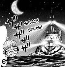
We've still seen no proof of Sai's mathematical ability apart from the flashback which could have been an exaggeration by Ryusui, so it's fair that Chrome and Chelsea seem to doubt his capabilities.

Senku says they need "someone" to be ready 24/7 to do quick calculations, however forcing someone to stay up for 24 hours to do stressful math is asking for a disaster. They would have always needed more than one person doing math for safety reasons, even to just compare answers.
(Also the concept of Whyman threatening them and/or attacking them even in space gets me excited!)
Thanks to Sai's petrification scars, he probably doesn't even need his charcoal pencils wrapped since the stain from the dust wouldn't show up on his hands!
Also, Sai is ambidextrous!
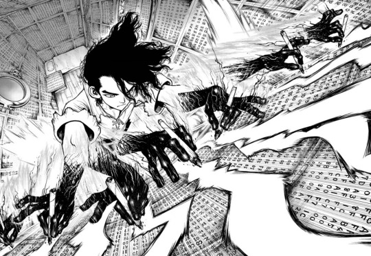
The code is mostly base16/hexadecimal (a combination of numbers between 0-9 and letters between A-F), however one of the panels seems to be base32 or something else since the letters M and K are present.
Another code, perhaps? 🤔
Low-level programming languages like machine code and assembly language are difficult to use. Even Inagaki agrees!
This change already happened last chapter, but Chrome's cross-body bags got an upgrade!
There's some old Norse runes carved into the sword, however at least two of the letters are flipped and trying to translate the rest seems to result in gibberish.
In Dragon Quest, the lettering usually simply reads "DRAGON QUEST" so maybe this somehow says "DOCTOR STONE"?

Unsurprisingly, the characters drawn here are inspired by real Dragon Quest characters.

The gaming system shown is the original Nintendo Entertainment System (NES): the Famicom. If you remember a differently-shaped NES, it's because it was replaced with a newer version for American markets.

20 notes
·
View notes